Showing posts with label CMOS. Show all posts

Friday, December 29, 2023

TSMC Set to Revolutionize Chip Technology with Trillion-Transistor Packages by 2030

In a groundbreaking announcement at IEDM, TSMC has unveiled ambitious plans to develop chip packages harboring over one trillion transistors and monolithic chips with more than 200 billion transistors by 2030. This visionary goal is set to be achieved through the development of advanced production nodes, including 2nm-class N2 and N2P, and even finer 1.4nm-class A14 and 1nm-class A10 processes. Despite the slowdown in process technology development and existing technical and financial challenges, TSMC remains optimistic about accomplishing these targets within the next five to six years. The company, renowned as the world's largest semiconductor foundry, is confident in overcoming industry hurdles to bring these complex, multi-chiplet systems and more intricate monolithic chips to the forefront of technology. This development signals a significant leap in chip architecture, promising transformative advancements in the tech industry.


Source:

Saturday, October 21, 2023

Intel Unveils Breakthrough 3D CFET Design at IEDM: Setting the Stage for Next-Gen Compact and Efficient Electronics

Intel researchers developed a 3D monolithic CFET device* with 3 n-FET nanoribbons atop 3 p-FET nanoribbons, separated by 30 nm gap. This industry-first device enabled the creation of functional inverters at a 60 nm gate pitch. Notably, it incorporated vertically stacked dual-Source/Drain epitaxy, dual metal work function gate stacks, and backside power delivery with direct device contacts. They also introduced a nanoribbon "depopulation" method for varying n-MOS/p-MOS device numbers. This research advances the understanding of CFET scalability for logic and SRAM applications and highlights key process enablers. The paper will be presented at the upcoming IEDM conference in San Francisco.

Comment: The stacked CMOS inverter at a 60 nm gate pitch represents an advancement in semiconductor design, allowing for denser circuits. The 60 nm distance between gates indicates a highly miniaturized design. Power vias provide vertical power connections to different layers, while direct backside device contacts enhance efficiency and heat dissipation. This development offers a glimpse into the  future electronic devices being more compact, efficient, and high-performing than deploying "planar" designs in one layer like the FinFETs and GAA-FETs of today.

ALD plays a key role in manufacturing 3D monolithic CFET devices by assisting in crafting the architecture and providing atomically precise and even thin film layers at small scales. ALD ensures even coverage, which is important for 3D designs, especially on vertical areas and inside deep gaps. It's used to put down important materials in transistor gate stacks (High-k/Metal Gates or HKMG), as well as barrier and seed layers. ALD also helps in doping (SSD - solid state doping), which changes how semiconductors behave, and in creating spacers, important for separating and defining parts of transistors. In brief, ALD helps improve the CFET design and its overall performance.


Figures from IEDM press kit

* A 3D monolithic CFET device combines three-dimensional stacking and the Complementary Field-Effect Transistor (CFET) design within a single semiconductor structure. This approach vertically integrates both n-type and p-type transistors on the same substrate, promoting tighter integration and reduced interconnect delays. By leveraging the complementary operation of CFET and the benefits of 3D stacking, the device aims to enhance performance, miniaturization, and efficiency in semiconductor technology.

Wednesday, February 3, 2021

LIVE Stream - Advanced Process Technologies to Enable Future Devices and Scaling (invited), Rob Clark Tokyo Electron

SEMICON Korea SEMI Technology Symposium (STS) 2021 - The invited presentation titled "Advanced Process Technologies to Enable Future Devices and Scaling" can be streamed starting Feb. 3 in S. Korea (2/2 evening U.S.). 

This is an overview of new processing technologies required for continued scaling of leading-edge and emerging semiconductor devices. The main drivers and trends affecting future semiconductor device scaling are introduced to explain how these factors are influencing and driving process technology development. Topics explored in this presentation include atomic layer deposition (ALD), atomic layer etching (ALE), selective deposition and etching. In order to enable self-aligned and multiple patterning schemes as well as emerging devices for future manufacturing, atomic level process technologies need to be leveraged holistically. Real-world examples of current and future integration schemes, as well as emerging devices, will be presented and explained so that attendees can understand how advanced process technologies will be used in future device manufacturing as well as what benefits and tradeoffs may be encountered in their use.


Saturday, January 4, 2020

ASM International received TSMC’s Excellent Performance Award for ALD and Epitaxy products

ASM International N.V. (LINK) has received TSMC’s “Excellent Performance Award”, one of seven equipment suppliers to win this recognition in 2019. The award was presented to ASM by Mr. J.K. Wang, Senior Vice President Advanced Fab Operations, at the TSMC Supply Chain Management Forum on Dec 5, 2019, in Taiwan.

The award was received by ASM in recognition of its technology collaboration with TSMC. During the presentation, TSMC explained three points that contributed to the award to ASM. 

1) Outstanding development support.
2) Continuous efforts in productivity improvement.
3) Excellent delivery support on production ramp.

“On behalf of ASM and all of our employees, I thank TSMC for their recognition through this esteemed award,” said Chuck del Prado, CEO and President of ASM International. “Our partnership with TSMC is of strategic importance to ASM. We continuously focus on advancing our leading edge technology, including ALD and Epitaxy products and processes in support of our technology collaborations with TSMC."
 

ASM product portfolio for semiconducttor high volume manufacturing includes ewafer processing equipment for processes such as Atomic Layer Deposition (ALD), Plasma Enhanced ALD (PEALD), Epitaxy, Plasma Enhanced Chemical Vapor Deposition (PECVD), Low Pressure Chemical Vapor Deposition (LPCVD) and Oxidation/Diffusion. (source & credit www.asm.com)

Wednesday, June 19, 2019

TechInsights’ Logic, NAND, DRAM and Emerging Memory Process Roadmaps are here

TechInsights’ Logic Process Roadmap offers an assessment and the anticipatory timing of new innovations from key players within the Logic space including: TSMC, Global Foundries, Intel & others. Download the roadmap here

TechInsights’ technology roadmaps show you the innovations we are monitoring

For over 30 years, TechInsights has been reverse engineering semiconductors and advanced technology products, developing the world’s largest library of technical analysis. We have built this library through two approaches: by conducting analysis in response to client requests, and by proactively analyzing disruptive or innovative technologies as they are released.

We constantly monitor the consumer electronics market to determine which manufacturers are planning to release new solutions, and when. We maintain and regularly update technology roadmaps in several different areas: Logic, NAND Flash Memory, DRAM, Emerging Memory, and Internet of Things Connectivity Systems on Chips, and more.

Updates to the roadmaps shown below are released throughout the year; check this page for updates. 

Wednesday, May 8, 2019

4th CMC Conference Enabled Critical Information and Connections

Fab materials event in Albany, New York area April 25-26 featured GlobalFoundries keynote and Intel and TI presentations. Plan now for the 2020 April 23-24 event in Hillsboro, Oregon. 

(SAN DIEGO (PRWEB) May 07, 2019) Over 150 leading executives and managers within the semiconductor manufacturing ecosystem gathered on April 25th and 26th in the Albany area of New York state for an important event on fabrication (fab) materials. The fourth-annual Critical Materials Council (CMC) Conference, produced by TECHCET, included topical presentations, a fab tour, exhibits by specialty materials suppliers, and networking roundtable discussions to learn about best-practices in a pre-competitive environment. Folks who missed attending the event this year can register to access the posted presentations for a nominal fee at https://cmcfabs.org/cmc-conference-2019/.

The event opened again, as in each of the prior three years, on an extremely strong business and technology keynote address by an executive from one of the CMC Fab member companies. The 2019 CMC Conference keynote was given by Dr. John Pellerin, Deputy CTO and VP of Worldwide R&D, GlobalFoundries. Pellerin talked about how demand for new high-volume manufacturing (HVM) semiconductor devices over the next few years will drive needs for increased numbers of new specialty materials as well as volumes of existing materials in his presentation on "Materials Challenges & Opportunities in Differentiated Technologies."

In the first session of the event covering global supply-chain issues of economics and regulations, G. Dan Hutcheson, CEO of VLSI Research, presented on "Slowdown: When did it start? What drove it? And When will the recovery come?" Hutcheson showed data from leading economic indicators that the recent decline in global semiconductor fab industry revenues due to memory chip prices may have already turned around.

TECHCET Sr. Analysts Dr. Jonas Sundqvist and Terry Francis presented updated information on demand drivers and forecasts for ALD/CVD precursors and Rare Earths, respectively. Sundqvist--also leader of the Thin Film Technologies Group at Fraunhofer IKTS--focused on how new 3D memory and logic chips demand more deposition precursors such that chemical volume growth will outpace that of silicon wafers, shown in the Figure. Francis showed how "Rare Earth" elements are not so rare at the elemental level, but complex dynamics between mining and refining and capitalism have led to a situation where mainland China currently controls most of the market for elements such as lanthanum (used in advanced ICs to create CMOS logic gates). Deep dives into all such materials matters are found in the TECHCET Critical Materials Reports (CMR), and you can find all of them online at https://techcet.com/shop/

Global semiconductor silicon quarterly wafer shipments 2015-2019 in millions of square inches (MSI). (Source: TECHCET)
The 2020 spring CMC Conference is scheduled for April 24-25 in Hillsboro, Oregon. The CMC Fab members and Associate members will again gather for two days of private face-to-face meetings before attending the public CMC Conference.

In addition to the annual spring CMC Conference in the US, there is also an annual fall CMC Seminar in Asia. The 2019 CMC Seminar will be held on October 17 in Taoyuan, Taiwan. For more information on CMC events see https://techcet.com/cmc-events/.

About CMC:
The Critical Materials Council (CMC) of Semiconductor Fabricators (CMCFabs.org) is a membership-based organization that works to anticipate and solve critical materials issues in a pre-competitive environment. The CMC is a business unit of TECHCET, and includes materials supplier Associate Members.

About TECHCET:
TECHCET CA LLC is an advisory services firm focused on process materials supply-chains, electronic materials business, and materials market analysis for the semiconductor, display, solar/PV, and LED industries. Since 2000, the company has been responsible for producing the SEMATECH Critical Material Reports™, covering silicon wafers, semiconductor gases, wet chemicals, CMP consumables, Photoresists, and ALD/CVD Precursors. For additional information about reports, market briefings, CMC membership, or custom consulting please contact info(at)cmcfabs(dot)org, +1-480-332-8336, or go to http://www.techcet.com or http://www.cmcfabs.org.

Friday, March 15, 2019

Samsung’s GAA Transistor, MBCFET™ aims at Reduced Size and Increased Performance

While chipmakers are struggling with the FinFET based chip production below 5 nm process nodes, Samsung has planned to opt for GAA (gate all around) architecture. Samsung’s GAA redesigns the transistor, making it more power-efficient and better-performing than the existing Multi Bridge Channel FET (MBCFET™) that utilize stacked nanosheets. 
 
Samsung’s patented MBCFET™ is formed as a nanosheet, allowing for a larger current and simpler device integration. It allows to reduce the operating voltage below 0.75 V that had been extremely difficult with FinFET. This yields to 50% less power consumption or 30% more performance at 45% less chip area compared to 7 nm FinFET technology. Also, Samsung's GAA technology is compatible with current FinFET production line that means the today's fab running on mature process tools and methodology can be utilized for GAA transistors. Here is the infographic to learn more about how Samsung’s GAA is advancing the future of semiconductor technology.

Source: Samsung LINK

Written by : Abhishekkumar Thakur and Jonas Sundqvist
 

Thursday, January 25, 2018

High Dielectric Constant Materials for Nanoscale Devices and Beyond

Here is a nice review on the introduction of high-k materials in the semiconductor industry and a future outlook by Prof. Hiroshi Iwai at Tokyo and Prof. Akira Toriumi Institute of Technology and their partner Prof. Durga Misra at New Jersey Institute of Technology. Thank you for sharing this one Rob Clark! The paper is part of a winter special issue in Interface (by ECS) with focus on "Importance of dielectric science"  and is free for download.


The authors conclude that:
  • The step coverage advantage of atomic layer deposition (ALD and is possible for, high‑k migration to FinFET CMOS technology.
  • The use of high‑k on new semiconductor substrates such as III-V, Ge and 2D materials is currently being investigated and faces many challenges. 
  • The discovery of ferroelectric properties of HfO2 makes it viable for more potential applications.


High Dielectric Constant Materials for Nanoscale Devices and Beyond
Hiroshi Iwai, Akira Toriumi and Durga Misra

Electrochem. Soc. Interface Winter 2017 volume 26, issue 4, 77-81

Abstract: Tremendous progress of CMOS integrated circuits have been conducted by the down-scaling or the miniaturization of MOSFETs (Metal Oxide Semiconductor Field Effect Transistors). Ten years, ago, the huge direct-tunneling gate leakage current through the thin gate SiO2 film of 1 nm thickness made it impossible to further scale-down the MOSFETs, and replacing the SiO2 by HfO2-based higher-dielectric constant (high-k) material was the solution. In this paper, the history of high-k gate insulator film development and two topics from recent research results regarding ferroelectricity and reliability are described.

Thursday, December 14, 2017

Globalfoundrfies to use quad patterning and Cobalt contacts for 7nm

ZDNet reports: At IEDM Globalfoundries presented details of its 7nm process which promises a significant increase in density, performance and efficiency in comparison to the 14nm technology used to manufacture AMD processors, IBM Power server chips and other products. GlobalFoundries will start 7nm production using current lithography tools, though it plans to quickly move to next-generation EUV lithography to cut costs

Based on GlobalFoundries latest generation of 3D or FinFET transistors, the 7LP process has a fin pitch (the distance between the conducting channels) of 30nm, gate pitch of 56nm and a minimum metal pitch of 40nm--all of which are "significantly scaled from 14nm." GlobalFoundries said it tuned the fin shape and profile for best performance, but did not provide measurements for the width or height of the fins. The smallest high-density SRAM cell measures 0.0269 square microns.
 
Like Intel, GlobalFoundries will use self-aligned quad patterning (SAQP) to fabricate the fins, as well as double-patterning for metal layers, and has introduced cobalt metal contacts to reduce resistance.


Thursday, January 7, 2016

The Critical Materials Council to be managed by TECHCET in 2016

 The Critical Materials Council for Semiconductor Fabricators, originally established by ISMI/SEMATECH in the early 1990’s, will be managed by TECHCET CA LLC starting January 01, 2016. Under its new name CMC Fabs, the membership-based organization of semiconductor fab & fabless manufacturers will continue working to identify and remediate issues impacting the supply, availability, and accessibility of both current and emerging semiconductor process materials. In keeping with SEMATECH tradition, the work of the international council takes place in a non-competitive environment for the benefit of the semi device fabrication community. Topics addressed are identified and prioritized by the member companies.


The organization has a new website at cmcfabs.org, which includes an overview of the Council’s mission, news of upcoming events and a Members Only portal for access to minutes of monthly phone/WebEx meetings and workshop details. The site also features access for Members to the TECHCET Critical Materials Reports and the related quarterly updates.

The next face-to-face meeting of CMC Fabs will take place May 3-6, 2016 in Hillsboro, Oregon. The meeting will include the annual CMC Materials Seminar held on May 5-6 that is open to the public. Sessions include a market briefing, supply chain issues and methods, the evolution of emerging materials in ALD / ALE, and the materials revolution around carbon. Speakers will be drawn from fabs, suppliers and analysts to address topics of concern and interest to the Council, and the semiconductor materials supply chain.


CMC Fabs is a unit of TECHCET CA LLC, a firm focused on Process Materials Supply Chains, Electronic Materials Technology, Materials Market Research and Consulting for the Semiconductor, Display, Solar/PV, and LED Industries. The company has been responsible for producing the SEMATECH Critical Material Reports since 2000.

Wednesday, September 2, 2015

TiC PEALD workfunction tuning by SK Hynix and KAIST

Here is an interesting paper on TiC PEALD workfunction tuning by SK Hynix and KAIST. They show how the workfunction of  PEALD TiC film is affected by growth temperature and a tunable WF of TiC film is compatible with a gate-first and/or gate-last process.


TiC ALD was deposited by cycling TiCl4 and TMA, in this case TMA was used as a source of carbon and H2 as a reactant gas with a plasma power of 300 W and argon as a purge gas and carrier gas.The films were characterized as MOS capacitor consisting of a TiC/SiO2/Si stack and the WF was extracted classically by having various SiO2 thicknesses.

Temperature control for the gate workfunction engineering of TiC film by atomic layer deposition

Choong-Ki Kim,  Hyun Jun Ahn, Jung Min Moon, Sukwon Lee, Dong-II Moon, Jeong Soo Park, Byung-Jin Cho, Yang-Kyu Choi, Seok-Hee Lee, 
Abstract

The effects of the deposition temperature on titanium carbide film formed by atomic layer deposition are investigated for gate workfunction (WF) engineering. As the deposition temperature increases from 250 °C to 500 °C, the WF of the TiC decreases from 5.24 eV to 4.45 eV. This WF dependency on the deposition temperature is mainly attributed to the average WF of each orientation of the sub-planes of the TiC film. An investigation of a tunable WF is conducted through Auger electron spectroscopy, transmission electron microscopy, and X-ray diffraction.

Sunday, August 2, 2015

Improved gate oxide quality for PEALD TiN vs PVD TiN for FDSOI CMOS

Gate dielectric quality is critical for advanced device fabrication, especially for low power, low leakage devices. In a recent study MIT shows a improved gate oxide quality for PEALD TiN vs PVD TiN. Using an Oxford Instruments OpAL system for PEALD of TiN from  tetrakis(dimethylamido)titanium (TDMAT) and an H2/N2 plasma mixture as precursors and plasma magnetron sputtered TiN films deposited at 300 °C using an Electrotech Sigma system the investigation concluded that:

  • FDSOI transistors fabricated with either gate deposition process showed similar electrostatic performance.
  • Gate dielectric quality metrics were significantly better when PE-ALD TiN was used compared to plasma sputtered TiN.
  • A significant reduction in interface state density was inferred from capacitance-voltage measurements as well as a 1200× reduction in gate leakage current.
  • A high-power magnetron plasma source produces a much higher energetic ion and vacuum ultra-violet (VUV) photon flux to the wafer compared to a low-power inductively coupled PEALD source.
The study was conducted in The MIT Lincoln Laboratory Microelectronics Laboratory. The Lab has a fully depleted silicon-on-insulator (FDSOI) CMOS circuit prototyping capability.


MIT Lincoln Laboratory occupies 75 acres (20 acres of which are MIT property) on the eastern perimeter of Hanscom Air Force Base, which is at the nexus of Lexington, Bedford, Lincoln, and Concord. The MIT property and most of the Laboratory’s facilities are within the Lexington town boundaries.

Comparison of gate dielectric plasma damage from plasma-enhanced atomic layer deposited and magnetron sputtered TiN metal gates (OPEN ACCESS)


Christopher J. Brennan, Christopher M. Neumann and Steven A. Vitale

J. Appl. Phys. 118, 045307 (2015); http://dx.doi.org/10.1063/1.4927517

Fully depleted silicon-on-insulator transistors were fabricated using two different metal gatedeposition mechanisms to compare plasma damage effects on gate oxide quality. Devices fabricated with both plasma-enhanced atomic-layer-deposited (PE-ALD) TiN gates and magnetron plasma sputtered TiN gates showed very good electrostatics and short-channel characteristics. However, the gate oxide quality was markedly better for PE-ALD TiN.  A high-power magnetron plasma source produces a much higher energetic ion and vacuum ultra-violet (VUV) photon flux to the wafer compared to a low-power inductively coupled PE-ALD source. The ion and VUV photons produce defect states in the bulk of the gate oxide as well as at the oxide-silicon interface, causing higher leakage and potential reliability degradation.


The MIT Lincoln Laboratory Microelectronics Laboratory is a state-of-the-art semiconductor research and fabrication facility supporting a wide range of Lincoln Laboratory programs. The 70,000-square-foot facility has 8100 square feet of class-10 and 10,000 square feet of class-100 cleanroom areas. The Lab has a fully depleted silicon-on-insulator (FDSOI) CMOS circuit prototyping capability

Monday, July 27, 2015

Hynix high bandwidth memory in an AMD Radeon ALD High-k Fury

Check it out - this is like the coolest thing I have ever seen so far - the two leading ALD High-k products (DRAM & High performance CMOS) merged into one ultra high performance graphics chip by AMD. TechInsights has investigated the AMD Fury X cards in their lab  and published it in a series of articles in EE Times:

The Hunt for Hynix HBM - Hynix high bandwidth memory addresses bandwidth limitations


Accordingly, SK Hynix announced its high bandwidth memory (HBM) product in early 2014, claiming it to be the world’s first 8Gb module made using 2Gb, 20nm node, DDR4 SDRAM. Now the HBM modules has shown up in product - AMD’s Radeon 390X Fury X graphics card.


According to TechInsight : "Hynix disclosed a via middle process for their HBM in two papers (Electronics Components & Technology Conference 2013 and VLSI Tech. Digest 2014). The TSV openings are formed after the tungsten contacts to the gates and source/drain regions are made, using a Bosch TSV etch. An oxide liner is then deposited along the via sidewalls, lined with a Ta-based barrier and Cu seed layers, and filled with electroplated Cu. A thermal anneal process is used as a Cu stress relief. A CMP and etch process is used to thin the backsides of the DRAM wafer and expose the Cu TSVs. The backsides of the DRAM wafers are then passivated with oxide, followed by the formation of the backside micro bumps."


AMD Radeon Fury X (Source: TechInsights)


Some facts from the reports:

  • The GPU die has four Hynix HBM memory modules arranged around its perimeter. 
  • Both the GPU and the HBM modules are flip-chip bumped to a UMC fabbed interposer. 
  • The interposer is, in turn, bumped to a laminate substrate. 
  • The GPU itself is a massive measuring in at 23mm by 27mm large, and is believed to be fabricated using TSMC’s 28nm HKMG process.


"The GPU die is seen in the center of the module with four Hynix HBM memory modules arranged around its perimeter. Both the GPU and the HBM modules are flip-chip bumped to a UMC fabbed interposer. This interposer is, in turn, bumped to a laminate substrate. The GPU is massive measuring in at 23mm by 27mm large, and is believed to be fabricated using TSMC’s 28nm HKMG process." (EE Times, TechInsight)


Schematic cross section of HBM module. (Source: AMD HBM brochure, TechInsights)


Hynix HBM memory (Source: Package Analysis of the SK-Hynix HBM, TechInsights)


Thursday, July 23, 2015

EUV, Atomic Layer Processes and KLA to solve all all Fab Issues at 7 nm and 5 nm

Here is yet another great article in Semiconductor Engineering by Mark Lapedus on the "The race toward the 7nm logic node. He systematically go through and summarize all important issues and technologies and news from SEMICON West from EUV via ALD to KLA ;-)


New technologies after finFETs and how the industry is likely to get there if it can resolve some very tough issues.

The race toward the 7nm logic node officially kicked off in July, when IBM Research, GlobalFoundries and Samsung jointly rolled out what the companies claim are the industry’s first 7nm test chips with functional transistors.

They’re not alone, of course. Intel and TSMC also are racing separately to develop 7nm technology. And in the R&D labs, chipmakers also are working on technologies for 5nm and beyond. Needless to say, the timing and certainty of 7nm and 5nm remain unclear.

In any case, there are two basic transistor candidates at 7nm—the finFETand the lateral gate-all-around nanowire FET, sometimes called the lateral nanowire FET. And at 5nm, the industry is leaning towards the lateral nanowire FET.

[...]
  • Patterning and mask making - EUV, LER
  • Fab flow and variation - CMP
  • Selective processes - ALD, MLD, ALE
  • Interconnects - RC
  • Inspection and metrology - KLA
While you´re at it you should also read this article by Mark Lapedus : 

What Will 7nm And 5nm Look Like? - Delays at 10nm raise questions about what’s next.

http://semiengineering.com/moores-law-slips-again/

Today, the lateral nanowire FET is the sole option at 5nm, according to Imec. Vertical FETs, TFETs and the other technologies have been pushed out to 3nm (!)

Monday, July 13, 2015

GLOBALFOUNDRIES Launches Industry’s First 22nm FD-SOI Technology Platform in Dresden

GLOBALFOUNDRIES today launched a new semiconductor technology developed specifically to meet the ultra-low-power requirements of the next generation of connected devices. The “22FDX™” platform delivers FinFET-like performance and energy-efficiency at a cost comparable to 28nm planar technologies, providing an optimal solution for the rapidly evolving mainstream mobile, Internet-of-Things (IoT), RF connectivity and networking markets.

Flanked by two clean room engineers posing with 300 mm device wafers the Globalfoundries Managers Gregg Bartlett, Sanjay Jha (CEO) und Rutger Wijburg today announced at a press event that Globalfoundries will invest $250 million for 22nm FD-SOI production in Fab 1 Dresden, Germany.


Flanked by two clean room engineers posing with 300 mm device wafers the Globalfoundries Managers Gregg Bartlett, Sanjay Jha (CEO) und Rutger Wijburg (VP and General Manager Fab1, Dresden) announce that Globalfoundries will invest $250 million for 22nm FD-SOI production in Fab 1 Dresden, Germany. From the press conference in Dresden (photo by Heiko Weckbrodt, www.computer-oiger.de)

While some applications require the ultimate performance of three-dimensional FinFET transistors, most wireless devices need a better balance of performance, power consumption and cost. 22FDX provides the best path for cost-sensitive applications by leveraging the industry’s first 22nm two-dimensional, fully-depleted silicon-on-insulator (FD-SOI) technology. It offers industry’s lowest operating voltage at 0.4 volt, enabling ultra-low dynamic power consumption, less thermal impact, and smaller end-product form-factors. The 22FDX platform delivers a 20 percent smaller die size and 10 percent fewer masks than 28nm, as well as nearly 50 percent fewer immersion lithography layers than foundry FinFET.

“The 22FDX platform enables our customers to deliver differentiated products with the best balance of power, performance and cost,” said Sanjay Jha, chief executive officer of GLOBALFOUNDRIES. “In an industry first, 22FDX provides real-time system software control of transistor characteristics: the system designer can dynamically balance power, performance, and leakage. Additionally, for RF and analog integration, the platform delivers best scaling combined with highest energy efficiency.”

"The 22nm process overcomes some challenges at 28nm. The transistor is better and the 20 percent area scaling we get makes up for the cost of the substrate," Jha said. "That means we can offer better performance at the same cost as 28nm [alternatives to FD-SOI]," Jha added in EE Times Europe.


The Dresden Fab 1 with a capacity: 60,000 wafers/month (300 mm)Technology: 45nm to 28nm and now also 22 nm (www.globalfoundries.com)

22FDX leverages the high-volume 28nm platform in GLOBALFOUNDRIES’ state-of-the-art 300mm production line in Dresden, Germany. This technology heralds a new chapter in the “Silicon Saxony” story, building on almost 20 years of sustained investment in Europe’s largest semiconductor fab. GLOBALFOUNDRIES launches its FDX platform in Dresden by investing $250 million for technology development and initial 22FDX capacity. This brings the company’s total investment in Fab 1 to more than $5 billion since 2009. The company plans to make further investments to support additional customer demand. GLOBALFOUNDRIES is partnering with R&D and industry leaders to grow a robust ecosystem and to enable faster time-to-market as well as a comprehensive roadmap for its 22FDX offering. 

Full story here: http://globalfoundries.com/newsroom/press-releases/2015/07/13/globalfoundries-launches-industry-s-first-22nm-fd-soi-technology-platform


Furthermore, Rutger Wijburg, senior vice president and general manager of the Dresden Fab 1, acknowledged that Globalfoundries is taking part in European Commission administered projects such as Horizon 2020. "We plan to extend that activity," Wijburg said according to EE Times Europe. As far as I know one of them is WAY-TO-GO CMOS headed by ST Microelectronics

Sunday, July 12, 2015

GLOBALFOUNDRIES Webinar: Extending Moore's Law with FD-SOI Technology

"Extending Moore's Law with FD-SOI Technology" is part of the GLOBALFOUNDRIES Technical Webinar Series. Jamie Schaeffer, Ph.D. explains how FDSOI (Fully Depleted Silicon On Insulator) technology is extending the life of Moore's Law.

Only available by this link : https://www.youtube.com/watch?v=7VmQlpXKtHE#t=100


It has previously been announced this year that Globalfoundries will entry FDSOI at 22 nm and today there will be a press conference in Dresden in front of the Bundeskanslerin Angela Merkels visit to the Dresden Fab tomorrow (Fab 1).


News & Analysis

GlobalFoundries’ FD-SOI Revolution

6/23/2015 06:16 PM EDT 
7 comments
NO RATINGS

Thursday, July 9, 2015

IBM present the first functional 7nm FinFET Test Wafer

An alliance led by IBM Research today announced that it has produced the semiconductor industry’s first 7nm (nanometer) node test chips with functioning transistors. The breakthrough, accomplished in partnership with GLOBALFOUNDRIES and Samsung at SUNY Polytechnic Institute’s Colleges of Nanoscale Science and Engineering (SUNY Poly CNSE), could result in the ability to place more than 20 billion tiny switches -- transistors -- on the fingernail-sized chips that power everything from smartphones to spacecraft.


With 20+ billion transistors on new chip, that's a 50% scaling improvement over today’s tech (IBM, Twitter)

To achieve the higher performance, lower power and scaling benefits promised by 7nm technology, researchers had to bypass conventional semiconductor manufacturing approaches. Among the novel processes and techniques pioneered by the IBM Research alliance were a number of industry-first innovations, most notably Silicon Germanium (SiGe) channel transistors and Extreme Ultraviolet (EUV) lithography integration at multiple levels.


Professor Michael Liehr (left) of SUNY Polytechnic Institute's Colleges of Nanoscale Science and Engineering (SUNY Poly CNSE) and Bala Haran (right) of IBM Research inspect 7-nanometer wafer of test chips developed in alliance partnership between IBM and SUNY Poly CNSE. (IBM)

Industry experts consider 7nm technology crucial to meeting the anticipated demands of futurecloud computing and Big Data systems, cognitive computingmobile products and other emerging technologies. Part of IBM’s $3 billion, five-year investment in chip R&D (announced in 2014), this accomplishment was made possible through a unique public-private partnership with New York State and joint development alliance with GLOBALFOUNDRIES, Samsung, and equipment suppliers. The team is based at SUNY Poly’s NanoTech Complex in Albany.


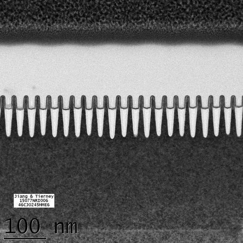
TEM image of IBM's 7-nanometer node finned field effect transistors (FinFETs) packed below 30-nanometer fin pitch using self aligned patterning. (IBM Research)

“For business and society to get the most out of tomorrow’s computers and devices, scaling to 7nm and beyond is essential,” said Arvind Krishna, senior vice president and director of IBM Research. “That’s why IBM has remained committed to an aggressive basic research agenda that continually pushes the limits of semiconductor technology. Working with our partners, this milestone builds on decades of research that has set the pace for the microelectronics industry, and positions us to advance our leadership for years to come.”


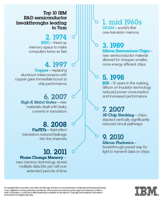
According to IBM the first  7nm chips announced, today was ably possible because of the past breakthroughs listed here (IBM, Twitter)

Microprocessors utilizing 22nm and 14nm technology power today’s servers, cloud data centers and mobile devices, and 10nm technology is well on the way to becoming a mature technology. The IBM Research-led alliance achieved close to 50 percent area scaling improvements over today’s most advanced technology, introduced SiGe channel material for transistor performance enhancement at 7nm node geometries, process innovations to stack them below 30nm pitch and full integration of EUV lithography at multiple levels. These techniques and scaling could result in at least a 50 percent power/performance improvement for next generation mainframe and POWER systems that will power the Big Data, cloud and mobile era.


Congratulations to Globalfoundries taking over IBM Chip buisness. Here is a picture from the cake eaten at Globalfoudries to celebrate (Picture from a friend).

“Governor Andrew Cuomo’s trailblazing public-private partnership model is catalyzing historic innovation and advancement. Today’s announcement is just one example of our collaboration with IBM, which furthers New York State’s global leadership in developing next generation technologies,” said Dr. Michael Liehr, SUNY Poly Executive Vice President of Innovation and Technology and Vice President of Research. “Enabling the first 7nm node transistors is a significant milestone for the entire semiconductor industry as we continue to push beyond the limitations of our current capabilities.”

"Today’s announcement marks the latest achievement in our long history of collaboration to accelerate development of next-generation technology," said Gary Patton, CTO and Head of Worldwide R&D at GLOBALFOUNDRIES. "Through this joint collaborative program based at the Albany NanoTech Complex, we are able to maintain our focus on technology leadership for our clients and partners by helping to address the development challenges central to producing a smaller, faster, more cost efficient generation of semiconductors." 

The 7nm node milestone continues IBM’s legacy of historic contributions to silicon and semiconductor innovation. They include the invention or first implementation of the single cell DRAM, the Dennard Scaling Laws, chemically amplified photoresists, copper interconnect wiring, Silicon on Insulator, strained engineering, multi core microprocessors, immersion lithography, high speed SiGe, High-k gate dielectrics, embedded DRAM, 3D chip stacking and Air gap insulators.

IBM and SUNY Poly have built a highly successful, globally recognized partnership at the multi-billion dollar Albany NanoTech Complex, highlighted by the institution's Center for Semiconductor Research (CSR), a $500 million program that also includes the world's leading nanoelectronics companies. The CSR is a long-term, multi-phase, joint R&D cooperative program on future computer chip technology. It continues to provide student scholarships and fellowships at the university to help prepare the next generation of nanotechnology scientists, researchers and engineers.

For more information about SUNY Polytechnic Institute, visit www.sunycnse.com andwww.sunypoly.edu.

Tuesday, July 7, 2015

Integration of Sub-10 nm ALD Gate Oxide on MoS2 with Ultra Low Leakage and Enhanced Mobility

Here is a nice Open Source report (Scientific Reports 5, Article number: 11921 (2015) doi:10.1038/srep11921) on integration of Sub-10 nm Gate Oxide on MoS2 with Ultra Low Leakage and Enhanced Mobility. 

Atomic layer deposition of Al2O3 on MoS2 flakes was performed according to the paper, some of the MoS2 flakes were loaded into the Picosun R200 ALD chamber for direct Al2O3 deposition. During the deposition, TMA and H2O served as the aluminum and oxygen precursors, respectively, and different growth temperatures and pulse time were adopted to observe their impacts. For some of the flakes, the remote O2 plasma pretreatments were carried out in the same chamber before Al2O3 was deposited.


(a) Cross-sectional schematic of the top-gated devices together with the electrical connections. (b) Ids – Vtg curves with Vds ranging from 50 mV to 500 mV. The inset shows the Ids – Vds curves with the top gate voltages of 0 V and 2 V. (c) Top gate leakage current of the device. Optical image of the top gate device is attached as the inset of (c). Top gate dielectric of this device is 60 cycles Al2O3 deposited with 60 s remote oxygen plasma pretreatment. All these measurements were performed at room temperature with the back gate grounded (Scientific Reports 5, Article number: 11921 (2015) doi:10.1038/srep11921) .

Sunday, June 21, 2015

A Novel ALD SiBCN Low-k Spacer for FinFETs presented at VLSI 2015 in Kyoto


A key challenge in reducing capacitance around the transistor is incorporating spacer and contact etch stop materials that are simultaneously low-k and robust to processing. One approach is to develop new low-k materials that can withstand the processing conditions [IEEE TRANSACTIONS ON ELECTRON DEVICES, VOL. 59, NO. 7, JULY 2012]


A Novel ALD SiBCN Low-k Spacer for FinFETs presented at VLSI 2015 in Kyoto by IBM and Globalfoundries. The abstract does not give too many details on the ALD process itself except that it is a "a novel low temperature ALD-based SiBCN material has been identified". However, the conference proceeding states that the SiBCN is deposited in a batch furnace:
  • SiBCN low k spacer was deposited in a batch furnace at 600 °C. The referral to low thermal process here may relate to earlier CVD processes at higher process temperatures.
  • The process was run in thermal ALD mode with alternating layers of BN and SiCN. 
  • The B/C ratio in the film was controlled by adjusting the BN:SiCN cycle ratio

A Novel ALD SiBCN Low-k Spacer for Parasitic Capacitance Reduction in FinFETs

T. Yamashita*, S. Mehta*, V. S. Basker*, R. Southwick*, A. Kumar**, R. Kambhampati*** , R. Sathiyanarayanan**, J. Johnson**, T. Hook*, S. Cohen*, J. Li*, A. Madan*, Z. Zhu*, L. Tai*, Y. Yao*, P. Chinthamanipeta*, M. Hopstaken*, Z. Liu*, D. Lu*, F. Chen**, S. Khan**, D. Canaperi*, B. Haran*, J. Stathis*, P. Oldiges*, C.-H. Lin*, S. Narasimha**, A. Bryant*, W. K. Henson**, S. Kanakasabapathy*, K. V. R. M. Murali**, T. Gow*, D. McHerron*, H. Bu* and M. Khare*, *IBM Research, **IBM SRDC and ***GLOBALFOUNDRIES, USA 

FinFET has become the mainstream logic device architecture in recent technology nodes due to its superior electrostatic and leakage control. However, parasitic capacitance has been a key performance detractor in 3D FinFETs. In this work, a novel low temperature ALD-based SiBCN material has been identified, with an optimized spacer RIE process developed to preserve the low-k value and provide compatibility with the down-stream processes. The material has been integrated into a manufacturable 14nm replacement-metal-gate (RMG) FinFET baseline with a demonstrated ~8% performance improvement in the RO delay with reliability meeting the technology requirement. A guideline for spacer design consideration for 10nm node and beyond is also provided based on the comprehensive material properties and reliability evaluations.

Thursday, June 18, 2015

Silicon Nanowire Remains Favorite to Replace FinFET

VLSI 2015 is going on and there are a lot of interesting information flowing from there and especially on the future of CMOS scaling. Here is a good article on what´s next after FinFET by Peter Clarke. He is claiming that Silicon Nanowires is the most probable path, i.e., not III/V on silicon: Silicon Nanowire Remains Favorite to Replace FinFET. The article is based on the published information and opinions from ARM, Imec, and Prof. Asenov and tries to give insights to some of the major questions and possible issues:
  • Vertical or Lateral?
  • With or without EUV?
  • What Material?
Below some of the statements made by the experts in the article by Peter Clarke. Please do read the article for the full story here (IHS Electronics360).


Prof. Asen Asenov of Glasgow University and CEO of Gold Standard Simulations

Asenov says, "I do not think that there is a real alternative to NWTs. They are a natural progression to FinFETs. Think of it like this: MOSFET—gate on the side of the channel; FinFET—gate on three sides of the channel; NWT or gate all around—gate on four sides of the channel." In a word, ultimate control of the current.


Aaron Thean, logic research director at IMEC.


"At IMEC we look at silicon, silicon-germanium and III-V channel materials but the preference is silicon." Other materials suffer from immaturity. "You have to ask what is the value proposition for these materials? SiGe improves mobility but there are issues of reliability. It is very difficult to passivate the surface." So for Thean, at least, progress is likely to be based in silicon with first-scaled FinFET. That means a taller fin, then movement to lateral nanowire transistors. But it still needs some level of innovation, he says.


Lucian Shifren, principal engineer at ARM.


"Gate-all-around silicon is most likely for a 'real' 7nm," Shifren says. He adds that the nominal 7nm would likely be a pseudo-scaled FinFET and that the nominal 5nm process would be gate-all-around.