%20(1).png)
Intel Foundry has demonstrated concrete momentum in de-risking 2D field-effect transistors as a future scaling path beyond silicon, through long-term collaboration with Imec. Results presented at IEDM show a world-first, 300 mm fab-compatible integration of key 2DFET modules, including source/drain contacts and gate stacks, using transition-metal dichalcogenide channels (WS₂ and MoS₂ for n-type, WSe₂ for p-type devices). The core innovation is a selective oxide etch applied to high-quality Intel-grown 2D layers capped with AlOx/HfO₂/SiO₂, enabling damascene-style top contacts while preserving the integrity of atomically thin channels.

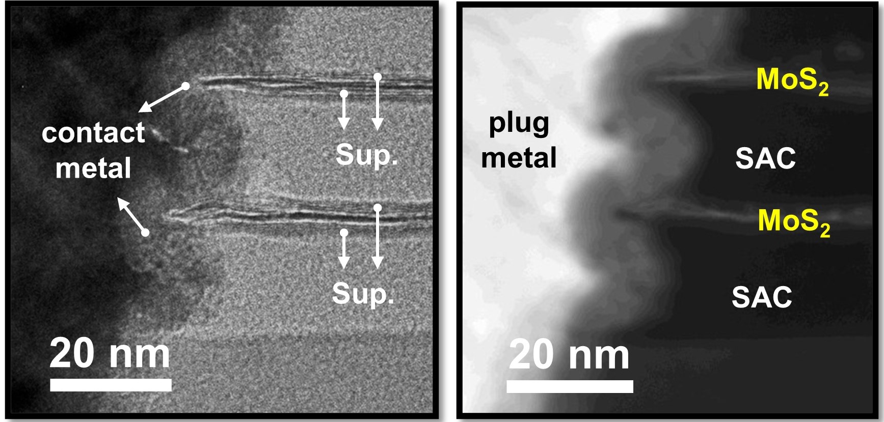
Fab-compatible 2D FET process integration demonstrated on 300 mm wafers. An imec-led research team reports new manufacturable process modules enabling scalable integration of 2D field-effect transistors in a 300 mm pilot line. Exploiting the strong chemical selectivity and anisotropic van der Waals structure of transition-metal dichalcogenides, the work demonstrates for the first time a selectively recessed oxide cap that enables damascene-style top contacts on monolayer WS₂, MoS₂, and multilayer WSe₂ channels, resulting in improved contact resistance. A replacement-oxide gate stack with scaled equivalent oxide thickness is also shown. In addition, a novel interlayer-selective removal process based on liquid intercalation reduces the top-gate capacitance-equivalent thickness from 2.5 nm to 1.5 nm. Together, these modules form fundamental building blocks for future 2D integration technologies. Top row: epitaxial TiN growth enabled by a 2D template (left, center) and chemical confirmation of a Ru top contact on a multilayer WSe₂ channel (right). Bottom row: schematic comparison of the baseline top-gate stack comprising interlayer, cap, and top-up oxides; full replacement-oxide process; and selective lateral interlayer removal from contact trenches. Based on Paper 10.1, “Selective Etch Process for Fab-Compatible Top Contacts, Replacement Oxide and Interlayer Removal in 2D FETs,” Q. Smets et al., presented at IEDM.
In parallel with its 2D transistor research, Intel Foundry has made significant progress in High Numerical Aperture EUV lithography as a cornerstone enabler for future device scaling. In close collaboration with ASML, Intel Foundry has completed acceptance testing of the TWINSCAN EXE:5200B, the most advanced High NA EUV scanner currently available. This system builds on the first-generation EXE:5000 platform while extending productivity to 175 wafers per hour and achieving overlay performance of 0.7 nm, metrics that are directly relevant to high-volume manufacturing rather than purely experimental use. Intel’s early access to High NA EUV, beginning with the first commercial installation in its Oregon R&D fab in 2023, positions the company as a lead development partner shaping how High NA lithography is qualified, integrated, and eventually deployed in production logic nodes.

Sources:
How Collaboration in High NA EUV and Transistor R&D Are Shaping Future Waves of Device Innovation