Lam Research’s dry resist technology represents a major shift in EUV lithography and semiconductor patterning, addressing critical challenges such as stochastic defectivity, resolution limitations, and cost-efficiency. With recent qualifications for advanced DRAM and 2nm logic manufacturing, along with a growing ecosystem for high-volume production, dry resist is positioned to disrupt traditional chemically amplified resists (CARs) and enable future High-NA EUV adoption.
One of the most significant recent developments is Lam’s qualification of dry resist for 28nm pitch BEOL logic at 2nm and below in collaboration with imec. This qualification confirms that dry resist can eliminate multi-patterning steps, reducing complexity and improving EUV throughput. The process is designed to work with both low-NA and high-NA EUV scanners, ensuring its relevance for sub-2nm logic scaling. This represents a key milestone in extending direct EUV printing to future logic nodes, an approach that could significantly lower lithography costs while improving pattern fidelity.

In addition, a leading DRAM manufacturer has selected Lam’s Aether dry resist technology as its production tool of record for advanced DRAM nodes. This decision highlights dry resist’s low-defect, high-fidelity patterning capabilities, which are essential for scaling memory architectures. The technology enables lower exposure doses while reducing stochastic defects, which are a major concern in EUV-based DRAM production. Given that Samsung, SK Hynix, and Micron are all increasing their reliance on EUV for next-generation DRAM, Lam’s dry resist is well-positioned for widespread adoption in the memory sector.

To ensure a stable supply chain for dry resist materials, Lam Research has partnered with Entegris and Gelest, a Mitsubishi Chemical Group company. This collaboration ensures reliable dual-source precursor production, providing chipmakers with long-term process stability. The partnership also focuses on the development of next-generation high-NA EUV precursors, further strengthening dry resist’s role in future sub-2nm manufacturing.
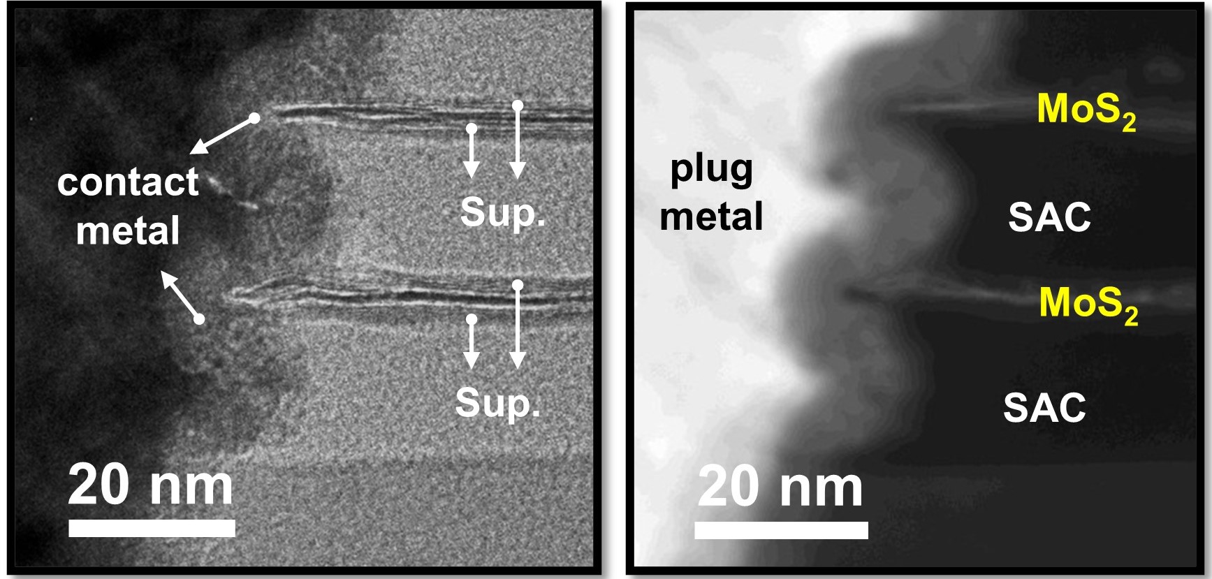
SEM images of 28 nm pitch line/space patterns imaged with 0.33NA EUV in dry resist from Entegris precursor.
A critical enabler of dry resist technology is its atomic layer deposition (ALD) process, which replaces traditional spin-coating used in CARs. ALD-based vapor-phase deposition offers higher uniformity, eliminating polymer chain variations found in conventional resists. It also allows precise thickness control, which is essential for optimizing EUV photon absorption and etch selectivity. Unlike CARs, which rely on a complex mixture of polymers, dry resist materials are based on single-component metal-organic precursors such as organo-tin oxides. These materials provide higher EUV photon absorption, improving sensitivity and pattern resolution.
Another key advantage of dry resist is its anisotropic dry development process, which replaces wet solvent-based development. Traditional CAR-based EUV resists require organic solvents or aqueous bases, leading to stochastic defects, material loss, and waste. Dry resist, by contrast, is developed entirely in the gas phase, selectively removing unexposed regions and forming a negative-tone image. This eliminates line collapse and delamination issues, improving yield stability. Additionally, the elimination of wet chemistries significantly reduces chemical waste, making dry resist a more sustainable solution with five to ten times lower material consumption compared to traditional resists.
Lam’s dry resist technology is poised to disrupt traditional CAR-based EUV lithography, particularly as the industry moves toward High-NA EUV adoption. By reducing multi-patterning dependency, the technology enhances cost-effective EUV scaling, making it an attractive solution for both logic and memory manufacturers. This positions Lam as a key leader in next-generation EUV resist solutions, challenging conventional resist suppliers like JSR, TOK, and Inpria.
From a sustainability perspective, dry resist significantly lowers EUV exposure dose requirements, leading to higher scanner throughput and lower energy consumption. Its reduced defectivity translates to higher yield per wafer, further enhancing cost-efficiency. The collaboration with Entegris and Gelest ensures supply-chain stability, making dry resist a viable and scalable technology for sub-2nm nodes.

The patent US20220020584A1 mentions several Lam Research tools that play a role in the dry resist deposition, patterning, and development process for EUV lithography. The Altus system is referenced for deposition, likely for metal or dielectric films in the dry resist stack, while the Striker plasma-enhanced atomic layer deposition (PEALD) system may be used for precise resist or underlayer deposition. The Versys platform, known for plasma processing, is relevant to the dry development process, and the Syndion system, typically used for deep silicon etching, may have applications in pattern transfer. Additionally, the Reliant tool is designed for volume manufacturing, possibly adapted for integrating dry resist technology, and the Kiyo plasma etch system is likely involved in etching after the dry resist development stage. These tools collectively enable Lam’s dry resist process to achieve improved resolution, defect reduction, and cost efficiency in advanced EUV lithography.
The patent US20220020584A1, filed by Lam Research Corporation, describes an innovative dry development process for EUV photoresists, which eliminates the need for traditional wet chemical development methods. The patent details a dry resist system deposited via vapor-phase precursors, forming a highly uniform, single-component material that enhances EUV photon absorption and sensitivity. The dry development process selectively removes unexposed resist regions using plasma-based or plasma-free chemical methods, significantly reducing line collapse and defectivity while improving resolution at sub-2nm nodes. By integrating dry resist deposition, EUV exposure, and dry development into a single cluster tool, the patented technology enables scalable, high-volume EUV manufacturing with lower chemical consumption and improved process sustainability, positioning it as a key enabler for High-NA EUV lithography.
Lam Research’s dry resist technology represents a significant development in EUV lithography by addressing key challenges in stochastic defectivity, process cost, and sustainability. Its qualification for 2nm logic and advanced DRAM manufacturing confirms its readiness for high-volume production. By utilizing ALD for precise resist deposition and securing a stable precursor supply through partnerships with Entegris and Gelest, Lam has established a strong foundation for scaling the technology.
Sources:
Lam Research Press Release on DRAM Adoption (Jan 2025):
Lam Researchimec Qualification of Dry Resist for 2nm Logic (Jan 2025):
imecEntegris and Gelest Collaboration Announcement (July 2022):
EntegrisOverview of Dry Resist ALD and Precursor Chemistry:
SemiAnalysisASML High-NA EUV Roadmap and Implications for Dry Resist:
ASML


%20(1).png)