Wednesday, May 22, 2019

SALDtech receives further funding to enable mass production of the next generation foldable OLED displays

SALDtech speeds up commercialization of Spatial Atomic Layer Deposition equipment for the display industry

Eindhoven, 22 May 2019 - SALDtech announced today that it has closed a second investment round with Innovation Industries, a leading high-tech VC fund and BOM, Brabant Development agency. TNO, through its subsidiary Holst Centre, has invested over 10 years in developing a new technology called Spatial Atomic Layer Deposition to produce large area ultra-thin layers with world class performance. SALDtech, a spin-off of TNO, will use the investment to develop and build production equipment to be integrated into the production lines of next generation flexible OLED displays for mobile phones, tablets, TVs and more. 
 

(Photo: TNO)
 
“We are very pleased with this investment as it enables us to further develop our product and speed up our sales” Huib Heezen, CEO of SALDtech states: “SALDtech will continue to cooperate closely with TNO on process innovation and will use the expertise on high tech equipment as readily available in the Eindhoven area for our product development. We are delighted to now have two top Dutch investors in the form of Innovation Industries and BOM on board who are committed for the long term.”


“We are excited that we have been a part of SALDtech since its first round last year and that we can continue to support SALDtech’s growth by participating also in this financing round”, says Nard Sintenie, Partner at Innovation Industries. “SALDtech’s technology has the ability to change the way we are working and interacting with displays and thereby addresses a huge market.”

“SALDtech has the potential to become the leading supplier in the display market” according Jurgen Van Eck, Senior investment manager at BOM Brabant Ventures“ As such, the company will play an important role towards local suppliers. We are happy we are able to contribute towards the further development of SALDtech”

Founding institute TNO is delighted with the opportunity this second financing round offers to SALDtech. “Both Innovation Industries and BOM have multiple investments in TNO spin-offs, , which shows the potential of the research we are doing at Holst Centre and TNO for the Dutch high tech industry. This investment is the next step in strengthening the Dutch economic position and Brainport in particular.” says Jaap Lombaers, Director at TNO.

About SALDtech

SALDtech BV is a spinoff from the Netherlands Organisation for Applied Scientific Research (TNO) and is based in Eindhoven, The Netherlands. The company was founded in 2018 to further develop, build and sell commercial Spatial Atomic Layer Deposition (SALD) systems into the flat panel display industry. The SALDtech tool will help enable the production scale up of next generation display technologies. Related end product display markets include smartphones, tablets, TV’s as well a new form factor displays in (autonomous) cars and on practically every surface.

Contact:
Huib Heezen (CEO)
huib.heezen@saldtech.com
+31 (0)6 30615028

Picosun provides the leading thin film coating solutions for medical industries

(Picosun, 21 May 2019) Picosun is the leading provider of AGILE ALD™ (Atomic Layer Deposition) thin film coating technology for healthcare industries. Picosun’s biocompatible ALD coatings enable safer and longer lasting products, more compact sensing, therapeutic, and analysis devices, and novel medical applications such as micro implants, smart ablation catheters, and deep brain stimulation probes. Picosun’s PicoMEDICAL™ ALD solutions are already in production use in healthcare industries in depositing bioactive coatings on surgical implants and functionalizing the surface of drug particles for controlled drug delivery.
Application examples:

Dental and orthopedic implants, surgical fixators Read more 

•    Improved osteointegration with bioactive TiO2 thin films
•    Biobarriers for encapsulation against metal ion leakage into tissue fluid


Pacemakers and other implantable electronic devices, microimplants Read more 
  • Hermetic biobarrier encapsulation of the device electronics against the effect of tissue fluid
Others
  • Medical MEMS, sensors, and Lab-on-a-Chip devices
  • Controlled/targeted drug delivery
  • Hydrophobic/hydrophilic coatings
  • Functional coatings on powder materials
  • Extremely thin films on stents

The PICOSUN™ P-300B and P-1000 large-scale batch ALD systems are specially designed for coating surgical implants, implantable medical devices, microimplants, and medical MEMS, sensors, and Lab-on-a-Chip devices.

Friday, May 17, 2019

Foldable Laptops Are On Their Way To Hit The Market By 2020 With Lenovo’s Unveiling Of The World’s First Foldable Laptop

ALD is know to be used in the OLED foldable display manufacturing as a moisture barrier mainly for foldable smartphones and other mobile devices. It’s not been many days of Samsung and Huawei unveiled their first foldable smart-phones: The Galaxy Fold and Mate X, respectively. Now Lenovo is jumping on board with a foldable laptop prototype in its ThinkPad X1 family powered by an Intel processor. For now, it’s just a prototype, but Lenovo may launch it for sale by 2020. The official visual preview can be seen here
 
 
Engadget (Youtube.com) "We got a chance to get our hands on Lenovo's new early prototype foldable PC. This device has some familiar features like an OLED screen and Bluetooth keyboard, but unlike other 2-in-1 laptops, the entire device can fold in half. This lets it fold up to around the size of a paper notebook for easy transport, or even lets you turn the bottom half into a keyboard you can type on. This is still early tech, but it's a look at what portable devices could be in the near future."
The prototype is with a 13.3″ screen that you can fold into the size of a compact 9.6″ Moleskine notebook. The laptop can be unfolded entirely and you can use the built-in kickstand on the rear to keep the screen standing up. You can also connect a Bluetooth keyboard to the device to use it as a traditional laptop; or, you can also just fold the screen halfway, and place it down on a table to use the bottom half as a virtual keyboard for typing. An attached stylus from Wacom can be utilized for super-accurate touch input or for virtual ink. The laptop also employs an attractive OLED screen (2K screen resolution, 4:3 aspect ratio) manufactured by LG display.


Lenovo doubles the number of hinge cycles it tests for its laptops to prevent the wear down of the foldable mechanism over time. Because it is under the ThinkPad name, the product will still need to pass Lenovo’s “rigorous” testing for ThinkPad category to ensure it’s just as durable. This is a Windows-based device, and Lenovo is working with Microsoft to make sure the software experience is optimized for this foldable format, for example, swapping to different modes needs to be seamless, and Windows needs to improve its tablet and touch interface to add value to this product. Moreover, the laptop has stereo speakers, an infrared camera, and two USB-C ports. Lenovo also claims it will offer an “all-day battery,” but there is no numeric figure out yet. 
 
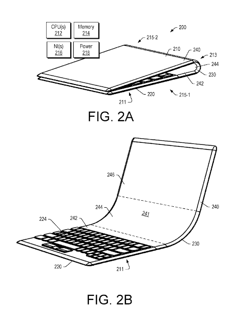
A patent application has just been published by the US Patent and Trademark Office, which comprises a foldable notebook with an OLED screen and a keyboard portion. Lenovo (Singapore) Pte. Ltd. US20190011955 DEVICE WITH FOLDABLE DISPLAY (LINK)
 
However, last Thursday, a senior Intel executive told the Nikkei Asian Review that the foldable laptops are at least two years away. "It's early path-finding now, and we are trying to understand the capability and the limitation of the [foldable] technology," Joshua D. Newman, Intel's general manager of mobile innovation and vice president of the company's Client Computing Group, said Wednesday on the sidelines of an Intel symposium in Taipei. (Link
 
----------
By Abhishekkumar Thakur and Jonas Sundqvist


Wednesday, May 15, 2019

RASIRC Enables Low Temperature Group III Metal-Nitride Deposition

Company highlights use of a novel hydrazine source at Compound Semiconductor Week

San Diego, Calif – May 15 2019 – RASIRC will introduce a novel hydrazine delivery system for reduced temperature Group III Metal-Nitride deposition at the Compound Semiconductor Week 2019 Workshop (CSW), Nara, Japan held May 19-23. RASIRC Chief Technology Officer Dr. Daniel Alvarez will present “Enabling Low Temperature Aluminum Nitride ALD by Use of a Novel Hydrazine Source” during the event’s poster session on May 21. The poster will compare growth characteristics and film properties for TMA/Brute Hydrazine versus TMA/Ammonia.

“There is an emerging need for low temperature III-Nitride deposition in order to prevent unwanted atomic diffusion of nearby metals and metal alloys. Utilization of hydrazine is thermodynamically more favorable due to the reactive nature of the N-N bond,” says Alvarez. “Hydrazine has been available commercially for many years, but not in a pure enough form needed for semiconductor manufacturing.” 


BRUTE Hydrazine Gas Superior to Standard 'anhydrous' hydrazine, which has a water concentration ranging from 0.2-2.0%. BRUTE Hydrazine has purity levels of less than 50ppm in the liquid phase and less than 1.0ppm in the gas phase. This makes BRUTE Hydrazine purity levels comparable to semiconductor grade ammonia. A higher reactivity compared to ammonia enables lower resistivity TiN films to be deposited by ALD at lower temperatures, which is essential for High-k/Metal Gate technology and metallization barrier/seed layers by ALD (Product description, LINK).


RASIRC President and Founder Jeffrey Spiegelman adds, “The use of hydrazine will enable our customers to have larger process windows while reducing costly precursor consumption found with sources like Indium.”

CSW Workshop is a joint venue for the 46th International Symposium on Compound Semiconductors (ISCS) and the 31st International Conference on Indium Phosphide and Related Materials (IPRM). ISCS is an international conference focusing on III-V, II-VI and IV-IV semiconductors and covers the scope of a variety of compound semiconductors used in modern electronic devices. IPRM is known as the leading worldwide conference on indium phosphide and related materials, from physics to its applications.

Dr. Alvarez will be available throughout the event to discuss the RASIRC precursor chemistry product line-up, which includes hydrazine, hydrogen peroxide and more. Information about RASIRC products will also be available in the Taiyo Nippon Sanso Corporation (TNSC) exhibition stand.

About RASIRC Products

BRUTE® Hydrazine enables uniform nitride deposition for Silicon and early transition metals at low temperature. BRUTE Hydrazine may also be used as an atomic hydrogen source, where metals such as Ru, Cu, and Co may be cleaned and reduced. Hydrazine gas is generated in situ and is virtually water free. Brute Hydrazine has been formulated for a relatively high flash point for safer handling.

BRUTE Peroxide is a novel oxidant that improves nucleation density at film interfaces when compared to other oxidants. Surface functionalization is more dense, and initiation is faster using anhydrous hydrogen peroxide gas compared with alternatives. This enables better selectivity and less damage to metal surfaces in ASD processes.

RASIRC Peroxidizer® provides high volumes of reactive H2O2/H2O mixtures for high throughput ALD. This reactive gas generator is ideal for roll-to-roll ALD coatings that require high speed deposition at reduced temperatures.

Additional RASIRC products include the RainMaker® Humidification System (RHS) and the Hydrogen Peroxide Steamer (HPS). The RHS generates water vapor for oxidation applications, and the HPS provides surface cleaning, preconditioning, wet thermal oxidation, and residual carbon removal.

About RASIRC RASIRC specializes in products that generate and deliver gas to fabrication processes. Each unit is a dynamic gas plant in a box — converting common liquid chemistries into safer and reliable gas flow for most processes. RASIRC technology delivers water vapor, hydrogen peroxide gas, and hydrazine gas in controlled, repeatable concentrations. RASIRC gas delivery systems, humidifiers, and closed loop humidification systems are critical for many applications in semiconductor, photovoltaic, pharmaceutical, medical, biological, fuel cell, and power industries. Call 858-259-1220, email info@rasirc.com or visit http://www.rasirc.com.

Sunday, May 12, 2019

Intel 2019 Investor Meeting: 7 nm Product in 2021

Intel held its 2019 investor meeting May 8, 2019 (LINK), it's first since 2017, and CEO Bob Swan announced that Intel would launch its 7 nm process in 2021 to challenge TSMC's 5 nm products.

Intel's Xe graphics will be the leading 7 nm product, which will come on the heels of Intel's first discrete 10 nm GPU that arrives in 2020. The company also unveiled its first block diagram of the Ice Lake architecture and announced that its new 10nm Tiger Lake processors will come to market in 2020.
Source: Tom´s Hardware LINK

 (intel.com)

----------
By Abhishekkumar Thakur

Wednesday, May 8, 2019

4th CMC Conference Enabled Critical Information and Connections

Fab materials event in Albany, New York area April 25-26 featured GlobalFoundries keynote and Intel and TI presentations. Plan now for the 2020 April 23-24 event in Hillsboro, Oregon. 

(SAN DIEGO (PRWEB) May 07, 2019) Over 150 leading executives and managers within the semiconductor manufacturing ecosystem gathered on April 25th and 26th in the Albany area of New York state for an important event on fabrication (fab) materials. The fourth-annual Critical Materials Council (CMC) Conference, produced by TECHCET, included topical presentations, a fab tour, exhibits by specialty materials suppliers, and networking roundtable discussions to learn about best-practices in a pre-competitive environment. Folks who missed attending the event this year can register to access the posted presentations for a nominal fee at https://cmcfabs.org/cmc-conference-2019/.

The event opened again, as in each of the prior three years, on an extremely strong business and technology keynote address by an executive from one of the CMC Fab member companies. The 2019 CMC Conference keynote was given by Dr. John Pellerin, Deputy CTO and VP of Worldwide R&D, GlobalFoundries. Pellerin talked about how demand for new high-volume manufacturing (HVM) semiconductor devices over the next few years will drive needs for increased numbers of new specialty materials as well as volumes of existing materials in his presentation on "Materials Challenges & Opportunities in Differentiated Technologies."

In the first session of the event covering global supply-chain issues of economics and regulations, G. Dan Hutcheson, CEO of VLSI Research, presented on "Slowdown: When did it start? What drove it? And When will the recovery come?" Hutcheson showed data from leading economic indicators that the recent decline in global semiconductor fab industry revenues due to memory chip prices may have already turned around.

TECHCET Sr. Analysts Dr. Jonas Sundqvist and Terry Francis presented updated information on demand drivers and forecasts for ALD/CVD precursors and Rare Earths, respectively. Sundqvist--also leader of the Thin Film Technologies Group at Fraunhofer IKTS--focused on how new 3D memory and logic chips demand more deposition precursors such that chemical volume growth will outpace that of silicon wafers, shown in the Figure. Francis showed how "Rare Earth" elements are not so rare at the elemental level, but complex dynamics between mining and refining and capitalism have led to a situation where mainland China currently controls most of the market for elements such as lanthanum (used in advanced ICs to create CMOS logic gates). Deep dives into all such materials matters are found in the TECHCET Critical Materials Reports (CMR), and you can find all of them online at https://techcet.com/shop/

Global semiconductor silicon quarterly wafer shipments 2015-2019 in millions of square inches (MSI). (Source: TECHCET)
The 2020 spring CMC Conference is scheduled for April 24-25 in Hillsboro, Oregon. The CMC Fab members and Associate members will again gather for two days of private face-to-face meetings before attending the public CMC Conference.

In addition to the annual spring CMC Conference in the US, there is also an annual fall CMC Seminar in Asia. The 2019 CMC Seminar will be held on October 17 in Taoyuan, Taiwan. For more information on CMC events see https://techcet.com/cmc-events/.

About CMC:
The Critical Materials Council (CMC) of Semiconductor Fabricators (CMCFabs.org) is a membership-based organization that works to anticipate and solve critical materials issues in a pre-competitive environment. The CMC is a business unit of TECHCET, and includes materials supplier Associate Members.

About TECHCET:
TECHCET CA LLC is an advisory services firm focused on process materials supply-chains, electronic materials business, and materials market analysis for the semiconductor, display, solar/PV, and LED industries. Since 2000, the company has been responsible for producing the SEMATECH Critical Material Reports™, covering silicon wafers, semiconductor gases, wet chemicals, CMP consumables, Photoresists, and ALD/CVD Precursors. For additional information about reports, market briefings, CMC membership, or custom consulting please contact info(at)cmcfabs(dot)org, +1-480-332-8336, or go to http://www.techcet.com or http://www.cmcfabs.org.

Tuesday, May 7, 2019

Demand for ALD equipment and Lumineq displays grows at Beneq

Beneq invests in R&D and production at the Home of ALD

Beneq®, a leading supplier of Atomic Layer Deposition (ALD) equipment and coating services, and the world’s premier manufacturer of thin film electroluminescent displays, has introduced a new investment plan to support growth in new industrial ALD solutions and the transparent display business. 

Following the agreement about the acquisition of Beneq Oy in September 2018, it was announced today that the new owners of Beneq have approved an investment program that allows Beneq to grow faster in its strategic focus areas, such as ALD solutions for the emerging semiconductor applications and transparent vehicle displays. 
 
 
Together with the new owners’ earlier investments in 2018 to improve Beneq’s equity ratio and working capital, the announced development programs result in a total investment of over 20 million euros. 

“When we invested in Beneq, we invested in people, technology know-how and innovation. The new growth plan will help us to realize the potential and achieve the ambitious growth targets we have set for Beneq,” commented Kong Jun, Chairman of Beneq.

New high-volume ALD manufacturing solutions for More-than-Moore applications

For the Atomic Layer Deposition business unit, the new growth program means major investments in new ALD solutions for the emerging semiconductor ALD business applications in the area of the so called More-than-Moore applications, such as MEMS, image sensors, power semiconductors and RF components needed for the future 5G and IoT solutions.

“Emerging semiconductor ALD and the diversified More-than-Moore applications are an extremely promising growth area for us. We have already had success in these areas with our latest flexible ALD cluster tools for high volume manufacturing. The new investment plan will allow us to fast-track our product development and services in these markets,” said Tommi Vainio, Vice President, Atomic Layer Deposition of Beneq.

Transparent displays for the automotive and transportation industries

For Lumineq Displays, the display business unit of Beneq, the investment plan allows both acceleration of product development in the area of transparent and in-glass displays, and improvements in Beneq’s display factory in Espoo, Finland.

“We have seen great interest in our transparent in-glass displays, especially in the transportation and automotive industries. The window-like transparency of Lumineq displays has helped our customers to build vehicles with improved safety and user experience and will serve as an important differentiation factor in their products,” said Petri Schroderus, Vice President, Lumineq Displays.

A recruitment campaign to support future growth

To enable future growth, Beneq has a continuous program to attract new talent. With the investment plan now approved, the company will start the next large recruitment campaign for building the talent pool. Most of the new positions will be in Espoo, Finland, but the plan also includes recruitment for Beneq’s international teams.


Applied Materials - The AI Era is Driving Innovations in Memory

[Applied Materials Blog] Industries from transportation and healthcare to retail and entertainment will be transformed by the Internet of Things, Big Data and Artificial Intelligence (AI), which Applied Materials collectively calls the AI Era of Computing.

The previous computing eras—Mainframe/Minicomputer, PC/Server and Smartphone/Tablet—all benefitted from advances in Moore’s Law whereby 2D scaling was accompanied by simultaneous improvements in performance, power and area/cost—also called “PPAC.”

While AI Era applications are booming, Moore’s Law is slowing; as a result, the industry needs breakthroughs beyond 2D scaling to drive PPAC in new ways. Specifically, we need new computing architectures, new materials, new structures—especially area-saving 3D structures—and advanced packaging for die stacking and heterogeneous designs.
 

The AI Era is Driving a Renaissance in Semiconductor Innovation (Applied Materials Blog)
 
AI Era architectural changes are influencing both logic and memory. Machine learning algorithms make heavy use of matrix multiplication operations that are cumbersome in general-purpose logic, and this is driving a move to accelerators and their memories. AI compute includes two distinct memory tasks: first, storing the intermediate results of calculations; and second, storing the weights associated with trained models.

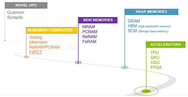
Performance and power are important in the cloud and in the edge, and innovations in memory can help. One approach using existing memory technologies is “near memories” whereby large amounts of working memory are condensed, placed in close physical proximity to logic, and connected via high-speed interfaces. As examples, 3D stacking and through-silicon vias are gaining traction. One major drawback of SRAM and DRAM as “working memories” in these applications is that they are volatile and need a constant supply of power to retain data—such as weights.

To reduce power in the cloud and edge, designers are evaluating new memories that combine high performance with non-volatility so that power is only needed during active read and write operations. Three of the leading new memory candidates are magnetic random-access memory (MRAM), phase-change RAM (PCRAM) and resistive RAM (ReRAM). 

Full article: Applied Materials Blog LINK
 
Additional read: Manufacturing Requirements of New Memories LINK