Tuesday, October 31, 2023

Micron's Distinct Approach to DRAM and Apple Design Wins

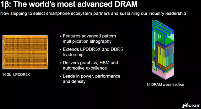
The tech landscape has seen consistent advancements, especially with the D1β (D1b) DRAM generation. Micron's D1β LPDDR5 16 Gb DRAM chips, integrated into the Apple iPhone 15 Pro, represent a significant step forward. Codenamed Y52P die, this chip offers an improved form factor and density, especially when contrasted with its LPDDR5/5X D1α 16 Gb predecessor. The integration of these chips into Apple's flagship device marks a significant design win for Micron, emphasizing the trust and partnership between the two tech giants.

In a recent teardown of the Apple iPhone 15 Pro, TechInsights has discovered a remarkable find - Micron's cutting-edge D1β LPDDR5 DRAM chips. These chips mark the industry's first foray into the D1β generation, and they are nothing short of impressive. (LINK)

Micron's technological direction is unique, especially with their decision to forego the Extreme Ultraviolet Lithography (EUVL) process, common in sub-15nm DRAM scaling. This stands in contrast to industry giants like Samsung and SK Hynix, who employ EUVL in their DRAM fabrication. Despite this, Micron has successfully launched the D1z, D1α, and D1β DRAM chips without EUVL, illustrating an alternative yet effective DRAM scaling approach.


In wrapping up, while Samsung and SK Hynix utilize EUVL in their DRAM processes, Micron has carved a different path, further solidified by their design wins with Apple. This partnership not only underscores Micron's technological prowess but also indicates the potential of varied methodologies in shaping the future of DRAM technology.


Source: Micron's D1β LPDDR5 Chip: Great Advancements in Memory Technology | Semiconductor Materials and Equipment (abachy.com)

Canon's Nanoimprint Leap: Challenging ASML's Dominance in Semiconductor Lithography

Canon Inc. has unveiled its semiconductor lithography equipment after 10 years of development, aiming to challenge the market dominance of Netherlands-based ASML Holding NV. This equipment, using Canon's new nanoimprint lithography (NIL) technology, prints intricate circuit patterns on semiconductor wafers. Historically, Japanese firms, including Canon, led the lithography market until ASML took over with a 90% share. Canon's system merges its renowned inkjet and camera tech. Unlike traditional methods using strong light and resulting in high costs, Canon's method is energy-efficient, printing patterns in a single step and using just 10% of the power. Its affordability and efficiency could make it competitive, especially for products with complex designs. While current cutting-edge devices use 2-nanometer chips, Canon's tech can produce 5-nanometer-node products, with aspirations to achieve 2-nanometer-node. Canon's launch offers potential diversification in a market long dominated by ASML.
According to Lithography expert Dr. Frederick Chen, Canon's statement on nanoimprint technology status following mid-October announcement indicated they were still facing challenges before reaching the levels required for mass production.


Thursday, October 26, 2023

Kokusai Electric's Stellar Tokyo IPO: A Surge in Stock, High Hopes for the Future

Kokusai Electric's stock rose 28% in its Tokyo debut after KKR sold its shares for $724 million, marking Japan's largest IPO in five years. Closing at 2,350 yen, Kokusai's valuation reached $3.61 billion. This was the biggest Tokyo listing since SoftBank Corp. in 2018. KKR reduced its stake from 73.2% to 47.7%. Analysts noted a challenging market for chip-related stocks but anticipate a rebound for Kokusai. The company specializes in machines for silicon wafer films, with major clients like Samsung. Despite a predicted profit drop, Kokusai's President sees growth potential by 2025. KKR's previous sale attempt to Applied Materials was unsuccessful. The IPO saw huge interest, with foreign investors oversubscribing by over 10 times.


Source: Kokusai Electric shares jump 28% in Tokyo debut - Nikkei Asia

Wednesday, October 25, 2023

Infineon Acquires GaN Systems for $830M, Bolstering Position in Power Semiconductor Market

Strategic Move Amplifies Infineon's GaN Expertise, Accelerating Energy-Efficient Solutions and Decarbonization Efforts

Infineon Technologies has successfully acquired GaN Systems, a Canadian company, for $830 million. This acquisition positions Infineon as a significant supplier of gallium nitride (GaN) power devices across various sectors, including consumer, industrial, and automotive applications. With the deal, Infineon inherits a wide array of GaN-based power conversion devices, designs, and advanced application expertise. GaN Systems, located in Ottawa, has integrated with Infineon, which already had its CoolGaN range. Jochen Hanebeck, Infineon's CEO, emphasized that GaN technology promotes energy efficiency and contributes to decarbonization efforts. Following this acquisition, Infineon boasts 450 GaN experts and access to over 350 GaN patent families, solidifying its leadership in the power semiconductor domain. The collaboration of both companies' intellectual properties, application insights, and customer projects optimally positions Infineon for future growth. 

Notably, GaN Systems has a unique island-based device structure that enhances power design performance, utilized by companies like QPT for fast switching speeds of up to 20MHz. This acquisition comes after Infineon's 2020 purchase of Cypress Semiconductor.

Source: Infineon completes acquisition of GaN Systems ... (eenewseurope.com)

Monday, October 23, 2023

TSMC To Report Breakthrough in NMOS Nanosheets Using Ultra-Thin MoS2 Channels at IEDM 2023

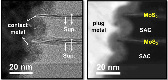
A TSMC-led research team, in collaboration with National Yang Ming Chiao Tung University and National Applied Research Laboratories, has unveiled promising results for using ultra-thin transition metal dichalcogenides (TMDs), specifically MoS2, as the channel material in NMOS nanosheets. Their innovative approach deviates from the conventional method of thinning Si channels. The team's devices exhibited impressive performance metrics: a positive threshold voltage (VTH) of ~1.0 V, a high on-current of ~370 µA/µm at VDS = 1 V, a large on/off ratio of 1E8, and a low contact resistance ranging between 0.37-0.58 kΩ-µm. These outcomes were primarily attributed to the introduction of a novel C-shaped wrap-around contact, which enhances contact area, and an optimized gate stack. While the devices demonstrated satisfactory mechanical stability, a challenge remains in addressing defect creation within the MoS2 channels. This groundbreaking study, titled "Monolayer-MoS2 Stacked Nanosheet Channel with C-type Metal Contact" by Y-Y Chung et al., is a pivotal step forward in nanosheet scaling using TMDs.


ALD is a the technique for the precise and uniform synthesis of MoS₂, especially for semiconductor applications on large-scale wafers. The choice of precursors plays a crucial role in achieving optimal deposition characteristics. Mo (CO) 6 and H2S have been identified as the primary precursors for depositing molybdenum and sulfur components, respectively. These precursors have demonstrated the capacity for self-limiting growth behavior within a specific ALD temperature window, leading to uniform MoS₂ layers. Notably, this process has been successfully scaled up to achieve highly uniform film growth on large 300 mm SiO2/Si wafers, marking its potential for industry-level manufacturing. The ability to maintain uniformity and thickness control on such wafers emphasizes the potential of ALD in integrating MoS₂ into next-generation electronic devices and further underscores the significance of selecting appropriate precursors for optimal deposition outcomes. Other precursors have been investigated. MoCl₅ and MoF₆ serve as alternative molybdenum sources. For the sulfur component, H₂S is commonly paired with molybdenum precursors, but (CH₃)₂S has also been explored. The choice of these precursors directly impacts the properties of the resulting MoS₂ film in the ALD process and therefore precursor development for 2D MoS2 is a hot field of ongoing research.

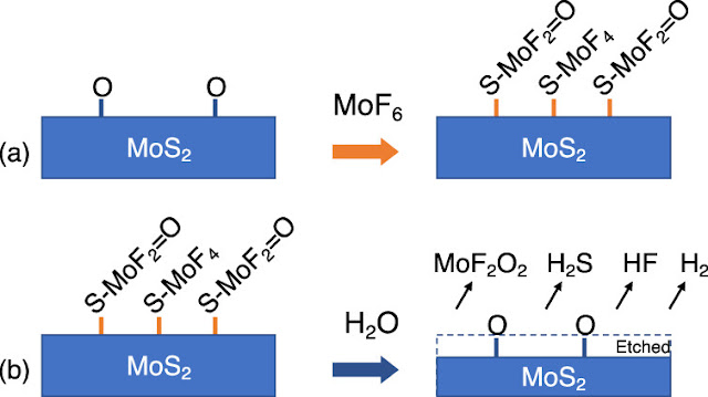
While deposition methods are abundant, etching processes are comparatively scarce. Recent research by Elton Graugnard et al also introduces a thermal Atomic Layer Etching (ALE) technique for MoS2, leveraging MoF6 for fluorination, alternated with H2O exposures, to etch both crystalline and amorphous MoS2 films. This process has been characterized using various analytical techniques like QCM, FTIR, and QMS. The etching is temperature-dependent, with a significant increase in mass change per cycle as temperature rises. The mechanism involves two-stage oxidation of Mo, producing volatile byproducts. The resultant etch rates were established for different films, and post-etch annealing rendered crystalline MoS2 films. The thermal MoS2 ALE introduces a promising low-temperature method for embedding MoS2 films in large-scale device manufacturing.


Sunday, October 22, 2023

Hamas' Brutal Attacks on Israel Could Disrupt Global Tech Supply Chain and Intel's Expansion Plans

The escalating Israel-Hamas war, after Hamas brutal attack on Israel and innocent civilians, is affecting the global tech sector. Many professionals, including top executives, are now serving as reservists in the Israel Defense Forces, as highlighted by EPSNews. Intel, a major private employer in Israel, along with other tech giants like Nvidia, Apple, Amazon, and Microsoft, faces potential disruptions, especially with facilities near conflict zones. The blockade in Gaza and transportation interruptions further strain the supply chain, emphasizing the tech industry's vulnerability to geopolitical challenges.


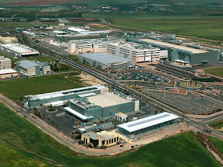
Intel factory in Kiryat Gat, employing about 5000 workers, which manufactures computer chips (wWikipedia), Location of Intel Fabs in Israel (Google)

Kiryat Gat, situated in Israel's Southern District, is known for Intel's semiconductor fabrication plants, including Fab 28 and the upcoming Fab 38. Founded in 1954, the city has grown significantly due to Jewish immigration over the decades and it remains an educational hub with 25 schools serving over 10,000 students.

The Israel-Hamas conflict has intensified concerns over the global semiconductor supply chain, as CNBC reports. With Israel being a key player in chip production, the geopolitical unrest poses risks to the semiconductor industry. The recent kidnapping of an Nvidia engineer further accentuates these threats, prompting tech firms to prioritize their employees' safety in the region.

Bloomberg reported this summer of Intel Corp.'s initiative to set up a new manufacturing facility in Israel. This move is part of Intel's strategy to diversify its production sources. While details remain undisclosed, the facility will focus on wafer fabrication. Intel's CEO, Pat Gelsinger, intends to expand manufacturing bases outside Asia. The plant, expected to operate from 2027, will be located in Kiryat Gat and is seen as a significant foreign investment in Israel. This development aligns with the global shift in chip manufacturing, as seen with Intel's investment in Poland and Micron Technology's potential investment in India.

Sources: 

China Tightens Grip on Vital Graphite Exports Amid Global EV Surge: Implications for U.S. Battery Industry and Beyond

From December 1, China will mandate export permits for certain graphite products to safeguard national security amidst increasing international scrutiny over its manufacturing dominance. China supplies 67% of global natural graphite and refines over 90% used in EV battery anodes. This move coincides with foreign governments pressuring Chinese firms on their industrial practices. The U.S. and European Union are implementing measures against Chinese products and technologies. New Western investments aim to counter China's graphite dominance, but success remains uncertain.


According to the USGS, in 2022, the United States did not produce any natural graphite. Instead, 95 U.S. companies consumed 72,000 tons of it, valued at $140 million. These companies were mainly located in the Great Lakes and Northeast regions. Natural graphite was used in batteries, brake linings, lubricants, steelmaking, and other applications. The U.S. imported an estimated 82,000 tons of graphite in 2022, with 77% being flake and high-purity graphite. Due to the rising electric-vehicle market, graphite consumption is expected to grow. Since 2018, the global battery market for graphite has surged by 250%. The U.S. has four operational lithium-ion battery plants and 21 more in development. These plants, when fully operational, will need about 1.2 million tons of spherical purified graphite annually, with 40%-60% sourced from synthetic graphite.

Source: USGS

U.S. graphite imports saw a decline in 2019 and 2020 but rose by 55% in 2022. This increase is attributed to the demand from the lithium-ion battery industry. China dominated the graphite production in 2022, accounting for 65% of the global output. North America's graphite production was just 1.2% of the global supply. Projects to explore and produce graphite are ongoing worldwide. The geopolitical conflict in Ukraine has impacted graphite production and trade relations, affecting the global graphite market.

Europe heavily relies on graphite imports, primarily from China, but aims to reduce this dependency by advancing local mining projects. The EU has categorized graphite as a critical raw material due to its importance in the EV battery sector. Notably, mining initiatives in Sweden, such as Woxna Graphite Mine, and Norway's Skaland Graphite operation are underway to bolster local supply chains. With the rise of European battery gigafactories, securing a stable graphite supply has become imperative.

Why is graphite important?

Graphite is a crucial component in electric vehicle (EV) batteries, specifically in the lithium-ion batteries that power most EVs. Here's how graphite is used:

Anode Material: In a lithium-ion battery, there are three primary parts: the cathode (positive electrode), the anode (negative electrode), and the electrolyte. Graphite is used as the primary material for the anode. When the battery is being charged, lithium ions move from the cathode through the electrolyte and get stored between the layers of graphite in the anode.

Conductivity: Graphite is a good conductor of electricity. This property is essential for efficiently moving electrons in and out of the anode during the charging and discharging cycles of the battery.

Stability: Graphite has a layered, planar structure. This allows lithium ions to easily slip between these layers, a process called intercalation. This structure provides a stable housing for lithium ions, ensuring the battery's longevity and safety.

Volume Expansion: One of the challenges with lithium-ion batteries is that materials can expand and contract significantly as they absorb and release lithium ions. Graphite's structure can accommodate this volume change, helping to maintain the integrity of the electrode.

Natural vs. Synthetic Graphite: There are two main types of graphite used in EV batteries: natural flake graphite and synthetic graphite. Both types can be processed to achieve the desired properties for battery anodes. While natural graphite is mined, synthetic graphite is produced from petroleum coke.

The increasing demand for EVs has led to a surge in the need for graphite. As a result, the sourcing, processing, and supply chain for graphite have become critical considerations for the battery and EV industries.

Sources:

China, top graphite producer, to curb exports of key battery material (cnbc.com)

Graphite (Natural) (usgs.gov)


New US Roadmap Identifies Critical Semiconductor Research Priorities

Advancing semiconductor research is essential to continued innovation in the chip industry and throughout our economy. As ever-shrinking semiconductor components face fundamental physical limits, next-gen breakthroughs are unachievable without major advancements. To help address this challenge, Semiconductor Research Corporation (SRC) today unveiled the Microelectronics and Advanced Packaging (MAPT) Roadmap, which defines critical chip research priorities and technology challenges that must be addressed to support the “seismic shifts” outlined in the Decadal Plan for Semiconductors released by SRC and SIA in January 2021.


The Decadal Plan identified five seismic shifts in the industry related to smart sensing, memory and storage, communication, security, and energy efficient computing. The MAPT Roadmap continues the spirit of the Decadal Plan and discusses how to achieve its system-level goals, outlining the implementation plan for the semiconductor industry. The fundamental research that will transform these obstacles is focused on advanced packaging, 3D integration, electronic design automation, nanoscale manufacturing, new materials, and energy-efficient computing. The MAPT Roadmap is framed around fundamental and practical limits of information and communications technology sustainability: energy sustainability, environmental sustainability, and workforce sustainability.


Federal government and private sector investments in semiconductor R&D have propelled the rapid pace of innovation in the U.S. semiconductor industry, spurring tremendous growth throughout the U.S. and global economies. Using the MAPT Roadmap as a guide, we must sustain and expand public and private investments in chip research to help unlock the transformative technologies of the future.

Source: SIA, Erik Hadland, Director of Technology Policy New Roadmap Identifies Critical Semiconductor Research Priorities - Semiconductor Industry Association (semiconductors.org)


Saturday, October 21, 2023

Intel Unveils Breakthrough 3D CFET Design at IEDM: Setting the Stage for Next-Gen Compact and Efficient Electronics

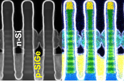
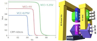
Intel researchers developed a 3D monolithic CFET device* with 3 n-FET nanoribbons atop 3 p-FET nanoribbons, separated by 30 nm gap. This industry-first device enabled the creation of functional inverters at a 60 nm gate pitch. Notably, it incorporated vertically stacked dual-Source/Drain epitaxy, dual metal work function gate stacks, and backside power delivery with direct device contacts. They also introduced a nanoribbon "depopulation" method for varying n-MOS/p-MOS device numbers. This research advances the understanding of CFET scalability for logic and SRAM applications and highlights key process enablers. The paper will be presented at the upcoming IEDM conference in San Francisco.

Comment: The stacked CMOS inverter at a 60 nm gate pitch represents an advancement in semiconductor design, allowing for denser circuits. The 60 nm distance between gates indicates a highly miniaturized design. Power vias provide vertical power connections to different layers, while direct backside device contacts enhance efficiency and heat dissipation. This development offers a glimpse into the  future electronic devices being more compact, efficient, and high-performing than deploying "planar" designs in one layer like the FinFETs and GAA-FETs of today.

ALD plays a key role in manufacturing 3D monolithic CFET devices by assisting in crafting the architecture and providing atomically precise and even thin film layers at small scales. ALD ensures even coverage, which is important for 3D designs, especially on vertical areas and inside deep gaps. It's used to put down important materials in transistor gate stacks (High-k/Metal Gates or HKMG), as well as barrier and seed layers. ALD also helps in doping (SSD - solid state doping), which changes how semiconductors behave, and in creating spacers, important for separating and defining parts of transistors. In brief, ALD helps improve the CFET design and its overall performance.


Figures from IEDM press kit

* A 3D monolithic CFET device combines three-dimensional stacking and the Complementary Field-Effect Transistor (CFET) design within a single semiconductor structure. This approach vertically integrates both n-type and p-type transistors on the same substrate, promoting tighter integration and reduced interconnect delays. By leveraging the complementary operation of CFET and the benefits of 3D stacking, the device aims to enhance performance, miniaturization, and efficiency in semiconductor technology.

Friday, October 20, 2023

The Semiconductor Showdown: TSMC's GAA FETs vs. Intel's RibbonFET

The semiconductor industry is witnessing a fierce competition between TSMC and Intel, as they advance transistor designs with TSMC's Gate-All-Around (GAA) FETs and Intel's RibbonFET. Atomic Layer Deposition (ALD) plays an instrumental role in crafting these intricate designs. As the race to dominate the microelectronics realm heats up, the innovations from these giants foretell a transformative phase for technology between 2024 and 2026. This article dives into their respective technologies, comparing their strategies and highlighting the future implications for the semiconductor industry.

Both TSMC and Intel are pushing the boundaries of semiconductor innovation with advanced transistor designs. TSMC's GAA (Gate-All-Around) FET (Field-Effect Transistor) technology and Intel's RibbonFET are prime examples of this evolution. ALD is crucial for GAA FET production, ensuring precision and atomically thin, conformal or on purpose non-conformal or selectively deposited films. As transistors miniaturized, ALD replaced traditional silicon dioxide gate dielectrics with high-k materials, reducing gate leakage and offering enhanced uniformity. One of the challenges in GAA FETs is accurately aligning the gate material around the channel; ALD facilitates this through self-aligned processes. Additionally, in configurations with multiple gates or nanosheets, ALD accurately deposits spacer materials, preserving the necessary separation between nanosheets. ALD also offers precise doping for GAA FETs, including NMOS and PMOS. With atomic-level control, ALD introduces dopants like phosphorus for NMOS and boron for PMOS. Given the shrinking device dimensions, ALD's precision becomes vital, especially when considering techniques like solid-state doping to achieve ultra-shallow profiles.


TSMC's Gate-All-Around (GAA) FET technology represents a significant shift from the traditional FinFET transistor design. In a GAA FET, the gate material wraps entirely around the channel, unlike the FinFET where the gate is only on three sides of a vertical fin. This complete encirclement provides enhanced control over the current flow through the channel, reducing leakage current and allowing for lower voltage operation. The result is improved energy efficiency and performance.


TSMC's roadmap to N2. (Image: TSMC)

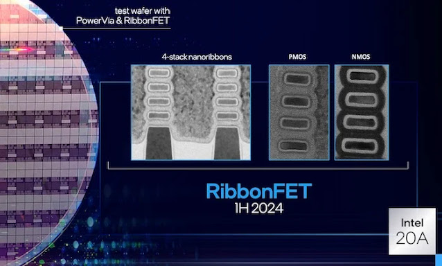
On the other hand, Intel's RibbonFET introduces a similar gate-all-around design but with a unique twist. Instead of a traditional vertical fin, RibbonFET uses nanosheet technology, where multiple flat nano-sheets are stacked to form the channel. This design offers even better control of the current flow, leading to significant gains in performance and efficiency. RibbonFET is one of Intel's flagship innovations for its advanced nodes, emphasizing the company's commitment to reclaiming technology leadership in the semiconductor space.


Intel 20A Ribbon FET (intel.com)

In a recent article Tom´s Hardware (Anton Shilow, link below) compares the advanced semiconductor technology nodes from industry TSMC and Intel, focusing on TSMC's N3P and N2 nodes against Intel's 20A and 18A nodes. Forecasted for release between 2024 and 2026, these nodes represent the forefront of semiconductor innovation. TSMC's N3P, a 3nm-class node, is set to be available by 2025 and offers performance comparable to Intel's 18A. Interestingly, TSMC's 2nm-class N2, expected in the second half of 2025, is anticipated to outpace Intel's 18A in terms of power, performance, and area advantages. Intel's 20A, arriving in 2024, promises significant advancements by introducing RibbonFET gate-all-around transistors and a backside power delivery network. The subsequent 18A will further refine these innovations. While TSMC leans on its proven FinFET technology for the N3P, it plans to introduce nanosheet GAA transistors in the N2. 

As the semiconductor race intensifies, both companies are heavily invested in outpacing each other, with TSMC focusing on technology maturity and cost-effectiveness, and Intel aiming to regain its technology leadership. The dynamics between these tech giants will shape the semiconductor industry's future.


Comparison of Advanced Semiconductor Technology Nodes: TSMC N3P & N2 vs. Intel 20A & 18A, highlighting the competitive landscape of the semiconductor industry for the years 2024-2026 based on Toms Hardware article below.

Sources: 

TSMC: Our 3nm Node Comparable to Intel's 1.8nm Tech | Tom's Hardware (tomshardware.com)

Intel and TSMC company web pages

Thursday, October 19, 2023

TSMC Foresees Stabilization in PC and Smartphone Demand; Remains Optimistic Amid Semiconductor Challenges

TSMC believes that the demand for personal computers and smartphones is beginning to stabilize after an extended downturn. During an earnings call, TSMC's CEO, C.C. Wei, stated that while there are early signs of stabilization in these markets, it's premature to predict a rapid recovery. There's been a notable decrease in global smartphone shipments, dropping from 1.4 billion units to 1.1 billion. However, there's been consistent demand in areas like artificial intelligence and high-performance computing, which are projected to stay strong through 2024-2025. Wei foresees potential for growth in 2024. 


He also commented on US export controls and their potential long-term effects. This comes after the US tightened regulations on AI chip exports to China, impacting major TSMC clients like Nvidia. Despite a 24.8% fall in TSMC's net profit for Q3, the company remains optimistic about its prospects, especially as it collaborates with Intel on chip production.

Jumpstart Your Semiconductor Career: ALD Process Engineer III Position in Santa Clara with Competitive Compensation and Benefits!

ALD Process engineer is the best possible start into a future career in the ever-evolving Semiconductor Industry. This Process Engineer III – (E3) position in Santa Clara, CA focuses on designing, analyzing, and troubleshooting complex problems within the semiconductor realm. Candidates should possess a Bachelor's Degree with 4-7 years of experience. The role includes a salary range of $116,000.00 to $159,500.00, potential bonus opportunities, and a comprehensive benefits package, with 10% travel time.

Apply here - Process Engineer III – (E3)


Stay informed in the ALD LinkedIn Group and chat with the hiring manager!


ALD TechDay at SEMICON Europa 2023 Hosted by Beneq

Join us for an exclusive expert forum discussing the adoption and applications of Atomic Layer Deposition (ALD) in the semiconductor industry. Powered by Beneq, this event is scheduled for Tuesday, November 14, from 3:00 pm to 5:30 pm at the Internationales Congress Center München (ICM).


Key Insights:

- Learn about the scaling of logic and memory semiconductor devices enabled by ALD.
- Discover ALD's rapid adoption in specialty device fabrication, particularly in wide-bandgap power semiconductors.
- Yole Group's projection reveals a 12% yearly growth in ALD equipment sales, reaching a record $680.5M by 2026.
- Get insights from industry experts, including speakers from Yole Intelligence, Beneq, and imec.
- Engage in discussions with a live panel of innovators and attend keynotes detailing innovative ALD applications, tool solutions, and case examples.

This event is tailored for integrated device manufacturers, foundries, and research and technology organizations. If you're invested in specialty semiconductor devices—from advanced packaging and CMOS image sensors to optoelectronics and power devices—this is an unmissable opportunity.

Attendance is complimentary but by invitation only. If interested, please register through our interest form.

Wrap up the day with the ALD TechDay networking gala dinner, a perfect platform for idea exchange and collaborative exploration.

*About Beneq:* A pioneering leader in atomic layer deposition, Beneq has been at the forefront since 1984. With a vast product range and unique development services, Beneq remains committed to simplifying ALD processes for researchers and shortening the time to market with its state-of-the-art ALD production.

ASML and Lam Research Navigate US Chip Restrictions with Continued Focus on China

The evolving landscape of the global semiconductor industry, marked by the escalating US chip curbs, has seen two industry leaders, ASML and Lam Research, maintain a significant focus on the Chinese market. ASML, the Dutch semiconductor behemoth, has reported a remarkable surge in its sales to China. As they dominate the market for DUV lithography machines, essential for chip production, sales to China for ASML soared to €2.44 billion ($2.58 billion) in the recent quarter, nearly doubling the figures from the previous one. Meanwhile, Lam Research, a US chipmaking equipment supplier for CVD, ALD and Etch, is experiencing a year-on-year decline in revenue by 31.4% to $3.5 billion in the quarter ending Sept. 24, remains buoyant about the Chinese market. With China accounting for a staggering 48% of its total revenue, up from 30% the previous year and 26% in the preceding quarter, CEO Tim Archer remains optimistic. He emphasized that the new U.S. export restrictions brought no unforeseen challenges and anticipates sustainable business growth in China, citing the country's long-term objectives.

Photo : ASML on X

However, it's not all smooth sailing. As the US and the Netherlands tighten their grip on chip equipment exports in an attempt to curb China's burgeoning semiconductor industry, challenges arise for these giants. Notably, Lam Research's shares fell by over 5% in extended trading after Archer's announcement. Furthermore, even though both ASML and Lam Research foresee continued demand from China, the trajectory remains uncertain with the intricate web of export controls and regulations. Still, with giants like KLA, Applied Materials, Tokyo Electron, and the aforementioned firms steering the ship, the semiconductor industry remains hopeful about navigating these turbulent waters.


ASML System sales by region 3Q/2023 (ASML.com)


Sources:

ASML stays optimistic on China as sales surge amid U.S. chip curbs - Nikkei Asia

Lam Research sees no material impact from new U.S. chip curbs - Nikkei Asia

Wednesday, October 18, 2023

Micron Unveils Breakthrough NVDRAM: A Dual-Layer 32Gbit Non-Volatile Ferroelectric Memory with Near-DRAM Performance

At the upcoming International Electron Devices Meeting (IEDM), Micron is set to present a paper on a novel 32Gbit non-volatile ferroelectric memory, termed NVDRAM. Authored by Nirmal Ramaswamy, the vice president of advanced DRAM and emerging memory at Micron, the paper is titled "NVDRAm: A 32Gbit Dual Layer 3D Stacked Non-Volatile Ferroelectric Memory with Near-DRAM Performance for Demanding AI Workloads". It introduces the world’s first dual-layer, high-performance, 32Gbit stackable ferroelectric memory technology. This technology, branded as non-volatile dynamic random access memory (NVDRAM), promises faster data movement and better energy efficiency than traditional DRAM, making it ideal for larger neural network models.

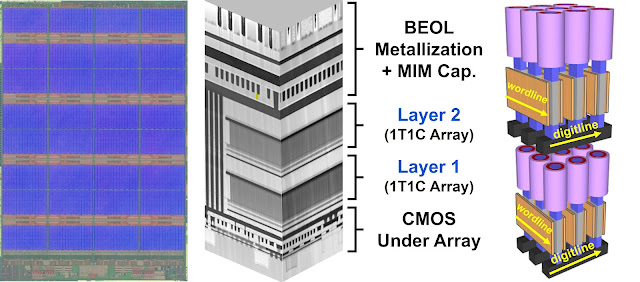
NVDRAM merges the benefits of ferroelectric memory cells – non-volatility and high endurance – with performance surpassing NAND flash memory retention and offering DRAM-like read/write speeds. The memory's architecture uses a 5.7nm ferroelectric capacitor for charge retention in a 1T1C DRAM structure, while dual-gated polycrystalline silicon transistors control access. The stacked double memory layer resides above a CMOS access circuit layer on a 48nm pitch. Despite the technological advancements, commercialization discussions remain speculative, potentially awaiting feedback from the IEDM presentation.


The images above show the final die layout (left) and SEM cross-section (center) of a 32Gb NVDRAM with 1T1C memory layers, fabricated over a CMOS array. On the right is a schematic diagram of NVDRAM memory arrays, showing polysilicon access device with orthogonal wordline (WL) and digitline (DL), and ferroelectric memory cells.

Abstract: Non-Volatile Ferroelectric w/DRAM-Like Performance, for AI & Machine Learning: Rapid growth in the size of the data models used in artificial intelligence (AI) and machine-learning (ML) applications is creating an urgent need for higher-bandwidth memory solutions. While new compute paradigms like near-memory-compute and processing-in-memory are being investigated, the best near-term opportunity is to outfit existing, traditional compute architectures with more efficient memory for faster data movement and to accommodate larger models. In this year’s Generative AI Focus Session, Micron researchers will unveil a memory technology for these uses which they call NVDRAM. It is the world’s first dual-layer, high-performance, high-density (32Gb), stackable and nonvolatile ferroelectric memory technology. It combines the non-volatile, high-endurance nature of ferroelectric memory cells with DRAM-like read/write speeds and endurance, and also surpasses the retention performance of NAND memory. NVDRAM uses an ultra-scaled (5.7nm) ferroelectric capacitor as the memory cell, and a dual-gated, stackable, polycrystalline silicon transistor as the access device. To achieve high memory density, two memory layers are fabricated above CMOS circuitry in a 48nm pitch, 4F2 architecture. Full package yield is demonstrated from -40°C to 95°C, along with reliability of 10 years (for both endurance and retention).

Sources:

Monday, October 16, 2023

Kokusai Electric's Successful IPO Raises $724.4 Million, Japan's Largest in 5 Years

Japanese chip equipment manufacturer Kokusai Electric has successfully raised $724.4 million through its initial public offering (IPO) by pricing its shares at the top end of a reduced marketing range. The IPO, Japan's largest in five years, saw Kokusai Electric value its shares at 1,840 yen per share, giving the company an overall valuation of 423.9 billion yen ($2.84 billion). The decision to lower the price range was influenced by the underwhelming performance of chip designer Arm's shares following its recent listing. Kokusai Electric's shares are set to debut on the Tokyo exchange's Prime Market on October 25. The company's major customers include Samsung Electronics, TSMC, and Micron Technology, accounting for over 40% of its revenue.


TSURUGI-C²® is a KOKUSAI ELECTRIC’s new thermal processing platform which is most recently developed for advanced devices especially for the ones with high aspect ratio 3D structures requiring high quality, uniform and conformal film deposition with new innovative reactor design and process techniques.

Kokusai Electric specializes in deposition and treatment process equipment for semiconductor manufacturing. Their deposition equipment is designed for creating nanoscale thin films on semiconductor wafers and supports technologies like LP-CVD, oxidation, annealing (low and high temperature), diffusion, and ALD. Notable products include TSURUGI-C², designed for advanced devices with complex 3D structures, AdvancedAce®-300 for batch thermal processing of 300mm wafers, and VERTRON® Revolution for 200-mm batch thermal processing.

Kokusai Electric's treatment equipment improves film properties through processes like nitridation, oxidation, curing, and annealing. MARORA® is ideal for gate dielectric film formation, utilizing plasma with low electron temperature. TANDUO® offers modular single-wafer treatment for various processes, and AdvancedAce®-300 supports LP-CVD, oxidation, annealing, and diffusion.

These equipment offerings are essential for semiconductor manufacturing, enabling the production of high-quality, high-performance components used in diverse electronic devices.

Sources:

US Researchers Achieve Record 25.1% Efficiency with Large Perovskite-Silicon Tandem Solar Cell

US scientists have achieved a breakthrough in photovoltaic (PV) cell technology by creating a large-area perovskite-silicon tandem solar cell measuring 24 cm2. This tandem cell has achieved a remarkable steady-state power conversion efficiency of 25.1%. To overcome common issues associated with scaling up perovskite solar technologies, such as shunting losses that create alternate pathways for solar-generated charge and lead to power losses, the researchers inserted a lithium fluoride (LiF) interlayer between a hole transport layer (HTL) and a wide bandgap (WBG) perovskite absorber. This interlayer improves physical contact and reduces shunting. The tandem cell demonstrated an efficiency of 25.2% under standard conditions, making it one of the most efficient two-terminal tandem devices for areas exceeding 10 cm2. This development holds promise for efficient, reproducible, and large-scale perovskite-silicon tandem solar cells.


Current-voltage curves for a perovskite mini-module with an aperture area of 42.9 cm2 Image: University of North Carolina at Chapel Hil, Cell Reports Physical Science, Creative Commons License CC BY 4.0

ALD is an important technology in perovskite solar cell fabrication. It enables precise, nanoscale control of layer thickness, ensuring uniform coverage even on complex surfaces. ALD is used for depositing passivation layers to reduce defects and enhance stability, creating protective barriers against environmental factors, engineering interfaces for improved charge transport, and ensuring compatibility with various materials. These applications contribute to improving the efficiency and long-term stability of perovskite solar cells, making ALD an essential tool in their development and optimization.

For deployment in solar cells, "perovskite" denotes a particular class of materials employed as the light-absorbing layer. These perovskite solar cells utilize a group of materials characterized by a crystalline structure akin to that of the mineral perovskite, named after Russian mineralogist Lev Perovski. Typically, these materials are comprised of organic-inorganic hybrid compounds, with common examples including methylammonium lead iodide (CH3NH3PbI3) and formamidinium lead iodide (HC(NH2)2PbI3). Perovskite solar cells have garnered substantial interest due to their potential for high efficiency, cost-effectiveness in production, and simplified manufacturing processes. Researchers are diligently working to enhance the efficiency, stability, and scalability of perovskite solar cells to position them as a competitive and sustainable renewable energy solution.