Showing posts with label Kokusai. Show all posts

Sunday, April 14, 2024

Kokusai Electric Showcased Batch ALD Technology for 40-28nm Nodes at SEMICON China 2024

At SEMICON China 2024, Kokusai Electric Corporation emphasized its strengths in atomic layer deposition (ALD) technology. The company showcased its batch-type ALD systems, which are particularly adept at achieving high-quality, uniform film deposition on multiple wafers simultaneously. This technology ensures excellent film thickness control and good step coverage, crucial for advanced semiconductor manufacturing. As the Chinese market increasingly transitions from chemical vapor deposition (CVD) to ALD due to its precision, Kokusai is poised to meet this rising demand, especially in fields like 3D stacking and miniaturization.


Kokusai highlighted its ALD technology specifically for mature semiconductor technology nodes in the 40 to 28nm range at SEMICON China 2024. This focus addresses the growing demand for precise film quality in these specific nodes within the Chinese market.


Thursday, October 26, 2023

Kokusai Electric's Stellar Tokyo IPO: A Surge in Stock, High Hopes for the Future

Kokusai Electric's stock rose 28% in its Tokyo debut after KKR sold its shares for $724 million, marking Japan's largest IPO in five years. Closing at 2,350 yen, Kokusai's valuation reached $3.61 billion. This was the biggest Tokyo listing since SoftBank Corp. in 2018. KKR reduced its stake from 73.2% to 47.7%. Analysts noted a challenging market for chip-related stocks but anticipate a rebound for Kokusai. The company specializes in machines for silicon wafer films, with major clients like Samsung. Despite a predicted profit drop, Kokusai's President sees growth potential by 2025. KKR's previous sale attempt to Applied Materials was unsuccessful. The IPO saw huge interest, with foreign investors oversubscribing by over 10 times.


Source: Kokusai Electric shares jump 28% in Tokyo debut - Nikkei Asia

Monday, October 16, 2023

Kokusai Electric's Successful IPO Raises $724.4 Million, Japan's Largest in 5 Years

Japanese chip equipment manufacturer Kokusai Electric has successfully raised $724.4 million through its initial public offering (IPO) by pricing its shares at the top end of a reduced marketing range. The IPO, Japan's largest in five years, saw Kokusai Electric value its shares at 1,840 yen per share, giving the company an overall valuation of 423.9 billion yen ($2.84 billion). The decision to lower the price range was influenced by the underwhelming performance of chip designer Arm's shares following its recent listing. Kokusai Electric's shares are set to debut on the Tokyo exchange's Prime Market on October 25. The company's major customers include Samsung Electronics, TSMC, and Micron Technology, accounting for over 40% of its revenue.


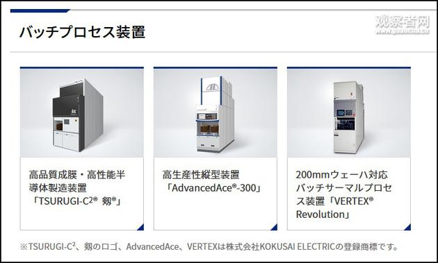
TSURUGI-C²® is a KOKUSAI ELECTRIC’s new thermal processing platform which is most recently developed for advanced devices especially for the ones with high aspect ratio 3D structures requiring high quality, uniform and conformal film deposition with new innovative reactor design and process techniques.

Kokusai Electric specializes in deposition and treatment process equipment for semiconductor manufacturing. Their deposition equipment is designed for creating nanoscale thin films on semiconductor wafers and supports technologies like LP-CVD, oxidation, annealing (low and high temperature), diffusion, and ALD. Notable products include TSURUGI-C², designed for advanced devices with complex 3D structures, AdvancedAce®-300 for batch thermal processing of 300mm wafers, and VERTRON® Revolution for 200-mm batch thermal processing.

Kokusai Electric's treatment equipment improves film properties through processes like nitridation, oxidation, curing, and annealing. MARORA® is ideal for gate dielectric film formation, utilizing plasma with low electron temperature. TANDUO® offers modular single-wafer treatment for various processes, and AdvancedAce®-300 supports LP-CVD, oxidation, annealing, and diffusion.

These equipment offerings are essential for semiconductor manufacturing, enabling the production of high-quality, high-performance components used in diverse electronic devices.

Sources:

Friday, September 22, 2023

Kokusai Electric's Upcoming IPO: A Strategic Move in the Booming Semiconductor Market

Kokusai Electric is set to go public on the Tokyo Stock Exchange on October 25th, with an indicative share price of 1,890 yen per share. The IPO aims to raise 111.2 billion yen ($749.88 million) to fund research investment in the chipmaking equipment market. This move also serves as a partial exit for KKR, which previously purchased Hitachi's electronic equipment unit in 2017 and later spun off Kokusai.

In 2019, KKR attempted to sell Kokusai to Applied Materials for $3.5 billion, but the deal fell through due to regulatory hurdles in China. Applied Materials subsequently acquired a 15% shareholding in Kokusai. Kokusai Electric specializes in semiconductor manufacturing equipment, particularly in Atomic Layer Deposition (ALD) technology, with a strong market position, including a 23% share of the global ALD equipment market in 2020.


Kokusai Electric's ALD equipment portfolio includes products like TSURUGI-C²® for 300mm wafers and VERTRON® Revolution for 200mm wafers, known for their high performance and productivity. The company's main customers for ALD equipment include Samsung, SK Hynix, Micron, and Intel. Kokusai Electric's IPO is scheduled for September 23, 2023.

Saturday, December 17, 2022

Kokusai Electric relies on patterned 3D substrates in thin film process metrology from Chipmetrics

Kokusai Electric is one of the leading semiconductor thin film process equipment manufacturers in the world. Recently, in the context of Japan Society of Applied Physics 69th Spring Meeting 2022, Kokusai presented their advanced thin film measurement and analysis concept used in their semiconductor process development.

The concept focuses on film thickness and localized film composition measurements from the special designed 3D patterned substrates, where the patterns are fine high aspect ratio structures.

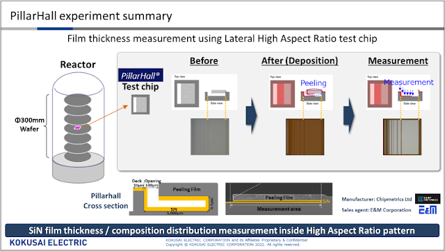
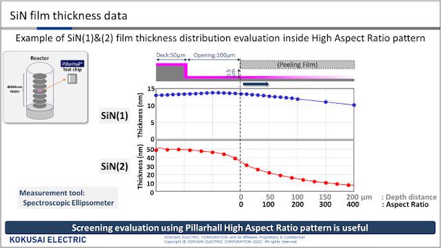
The average film thickness is obtained indirectly by measuring the mass change in the special 3D patterned wafer before and after the film depositions. The thickness accuracy is further improved by taking into account the high aspect ratio and wafer level non-uniformity measured by PillarHall® Lateral High Aspect Ratio (LHAR) test chips positioned on the carrier wafer. The PillarHall® measurement, enables easy screening after peeling off the top roof membrane and by measuring the film thickness distribution and conformality by the ellipsometer line-scanning measurements.

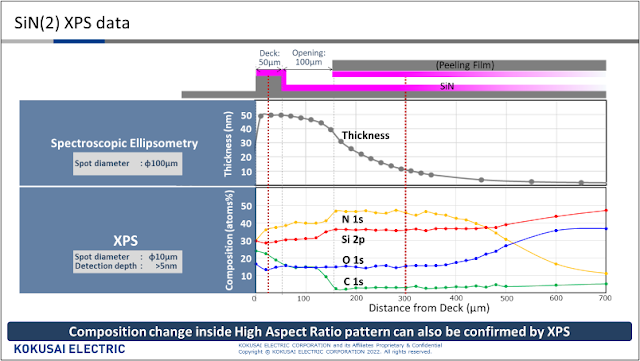
PillarHall® LHAR test chip has also another important function in Kokusai’s analysis concept. Namely, it is used for film elemental composition characterization along the trench wall in high aspect ratio structure. The measurement is carried out as a line-scan by XPS or SEM-EDS. For example, the characterization showed that two kinds of SiN processes behaved differently and Si/N composition changes along the high aspect ratio (AR>1000) trench were observed.


Figure 1. PillarHall experiment summary


Figure 2. SiN film thickness data


Figure 3. SiN(2) XPS data

Figures 1-3 show the PillarHall experimental set-up, data from the film thickness penetration depth profiles and XPS composition data of two kind of Kokusai’s SiN processes, SiN (1) and SiN (2).

Kenji Kameda and Akane Kitamura from Metrology Team, Kokusai Electric emphasized that:” It is difficult to obtain the analysis of thin films on high aspect ratio patterns without cross-sectional TEM. PillarHall is a simple and effective tool, it has fine patterns, and it enables us to use XPS and ellipsometer instead of TEM. Therefore, PillarHall is useful as an efficient measurement tool to improve Kokusai’s film forming technology.”

PillarHall LHAR test chip is a product of Chipmetrics Ltd, Finland. Chipmetrics CEO Dr. Mikko Utriainen reminds that any PillarHall data can be published without confidentiality concerns and the results are also well comparable between reactor systems and processes. The openness and accuracy of the ALD conformality data was one of the reasons why pioneering ALD scientists in Finland started to develop the PillarHall concept already in 2013.

Kokusai’s example shows that PillarHall is an efficient measurement tool and help to improve film forming technology for advanced semiconductor processes.

PillarHall is a product of Chipmetrics Ltd. Contact: info@chipmetrics, www.chipmetrics.com

Wednesday, March 24, 2021

Applied Materials may kill $3.5B buy of Japanese ALD and CVD Furnace Company Kokusai over delayed approval by China

Applied Materials Inc. on Monday said that its $3.5 billion offer to buy Kokusai Electric Corp. may be terminated because the deal hasn't been able to get timely approval from Chinese regulators. The Santa Clara chip manufacturing equipment company set a March 19 deadline on the deal late in December when it increased how much it would pay KKR HKE Investment L.P. for the Japanese company. The original price was $2.2 billion. But it said on Monday that it will likely now pay KKR a termination fee.


Trouble to reach approval in China has been foreseen by several analysts since the announcement 2019, see below for more details.

  • Kokusai is a small acquisition for Applied materials as compared to the previously failed mega-merger with Tokyo Electron
  • Kokusai, which counts Samsung, SK Hynix, Toshiba, and Micron among its top customers, reported revenue of $1.24 billion as of March 2018.
  • Kokusai’s batch wafer processing tools are less technology-intensive than Applied Materials’ single wafer tools, the recent focus on ultra-thin films has driven renewed interest in this group.
Background: 
  • Impacts of the US-China trade conflict on the semiconductor equipment market and ALD LINK
  • ASM International settles with Kokusai for Batch ALD patent licenses (US$61 million) LINK
  • Applied Materials to buy Japan's Kokusai to boost memory chip business and ALD LINK

Saturday, November 28, 2020

Applied Materials will regain its No. 1 ranking in the semiconductor equipment market in 2020 from ASML

According to recent published data by The Information Network (Seeking Alpha LINK), Applied Materials will regain its top ranking in the semiconductor equipment market in 2020 from ASML. Fab equipment spend in 2020 was enhanced from pull-ins of sales into China and Taiwan, with 3Q QoQ increases of 22.5% and 36.2%, respectively.

As is well known ASML and Applied Materials does not compete in their  business segments, Lithography (ASML) resp. Deposition & Etch (Applied Materials). Applied Materials has a number 1 spot in PVD, CVD, Epi, CMP and Implant/Doping. However, business segments where Applied Materials so far has not been successful to reach a top 3 position in the past years include:
  • Atomic Layer Deposition
  • MOCVD
  • Furnace 
  • Dielectric Etch  
  • Spray Processing
  • Dielectric Etch (including ALE)
  • Wet Stations
As is known, Applied Materials have several times made very serious attempts to enter the ALD segment, but failed several times to compete with ASMI, Tokyo Electron and the South Korean OEMs (Jusung Engineering, Wonik IPS and Eugene Technology. In 2019 Applied Materials announced that it will acquire Japanese Kokusai (LINK) but the final agreement is yet not settled. If successful Applied will have an opportunity to kill 2 birds with one stone:

1. Move in to top 3 spot in ALD
2. Take number 2 spot in Furnace business


Table based on information and own assumptions in the article (Seeking Alpha LINK)

Thursday, October 31, 2019

ASM International settles with Kokusai for Batch ALD patent licenses (US$61 million)

October 29, 2019, 12.15 p.m. CET (LINK) ASM International N.V. (Euronext Amsterdam: ASM) today announces that it has entered into a settlement agreement with Kokusai Electric Corporation (formerly known as Hitachi Kokusai Electric Inc. and hereinafter referred to as “KEC”) to resolve the arbitration proceeding relating to the license agreement which expired in November 2017. As part of this settlement, KEC will pay ASM an amount of US$61 million. With this settlement all pending disputes between ASM and KEC with respect to patent licenses have been resolved.

As announced on February 23, 2018, ASM initiated an arbitration proceeding on August 30, 2017 with the American Arbitration Association against KEC for breach of the license agreement between the companies. This license agreement provided KEC and its affiliates a license under certain patents of ASM in the field of Batch ALD. The companies have now entered into a settlement agreement concerning all the matters of the arbitration.

This arbitration settlement is separate from the settlement of all patent lawsuits and invalidation proceedings between ASM and KEC that was announced on July 1, 2019.

The settlement of the arbitration will positively impact ASMI’s sales and bookings in Q4 2019 with an amount of US$61 million, or approximately €56 million.
 
Background:

- Applied Materials to buy Japan's Kokusai to boost memory chip business and ALD (LINK)

- ASM International settles (US$115 million) with Kokusai Electric Corporation on the use and infringement of ALD patents  (LINK)


Tuesday, July 2, 2019

Applied Materials to buy Japan's Kokusai to boost memory chip business and ALD

Here are more details and analyst responses on the Applied Materials Kokusai purchase and my own thoughts at the end:

(Reuters, LINK) - U.S. chip gear maker Applied Materials Inc (AMAT.O) on Monday agreed to buy Japanese peer Kokusai Electric for $2.2 billion from KKR & Co Inc (KKR.N), as it bets on rising demand for memory chips used in data centers, 5G phones, and AI-powered devices.  

In summary:
  • Kokusai is a small acquisition for Applied materials as compared to the previously failed mega-merger with Tokyo Electron, meaning that the road to approval should be easy. However, China’s willingness from a political standpoint is always a risk, Evercore analysts said. 
  • Apart from China, the acquisition will need approvals from Israel, Ireland, Japan, Korea and Taiwan, Applied Materials Chief Financial Officer Dan Durn said on a call with analysts.
  • Kokusai, which counts Samsung, SK Hynix, Toshiba and Micron among its top customers, reported revenue of $1.24 billion as of March 2018. 
  • Kokusai’s batch wafer processing tools are less technology intensive than Applied Materials’ single wafer tools, the recent focus on ultra-thin films has driven renewed interest in this group, DA Davidson analysts said.
So this whole purchase is really about Applied Materials getting a state of the art ALD technology for the memory business (DRAM and 3DNAND). The last readout is a bit crazy, the analyst refers to ALD as an "Ultra Thin Films". Anybody who has followed the ALD business the previous 15-20 years know that Applied Materials has repeatedly failed to take a big market share in ALD and that a Japanese Large Batch ALD reactor is one of the most advanced and reliable ALD tools out there - simply because nobody would like to trash a full load of +100 product wafers. The top three domination has been by:
  • ASM International
  • Tokyo Electron
  • Kokusai
The top 3 has been followed by Lam Research, Jusung Engineering, Wonik IPS and Applied Materials was always somewhere in this bunch. Even the inrodcution of the new Spatial ALD Olympia platform didn´t change things. It seems that Tokyo Electron took a large part of the spatial ALD market with their NT333 tool and ASM was able to defend their single wafer approach by making the XP platform super productive by adding more chamber slots (up to 16 for the latest ASM XP8 QCM).  

When it comes to IP in Spatial ALD, Tokyo Electron is No.1 followed by Applied Materials (see below).

IP Applications for spatial ALD

Magically, Kokusai settled the IP issues with ASM just before the Applied announcement (LINK). Historically, Kokusai has been masters in avoiding to call ALD ALD because of the IP situation. However, now there is a different situation and Kokusai also have single wafer ALD out there, and Applied is dominating the BEOL films deposition business so we can assume that Applied will enter top three and have a go at No 1. Exciting!

Monday, July 1, 2019

Applied Materials to Acquire Kokusai Electric and enter the Large Batch CVD and ALD market

SANTA CLARA, Calif., July 01, 2019 (GLOBE NEWSWIRE) -- Applied Materials, Inc. (“Applied”) (Nasdaq: AMAT) today announced a definitive agreement under which Applied will acquire all outstanding shares of Kokusai Electric Corporation (“Kokusai Electric”) for $2.2 billion in cash from global investment firm KKR.

Kokusai Electric is a leading company in providing high-productivity batch processing systems and services for memory, foundry and logic customers. These systems complement Applied’s leadership portfolio in single-wafer processing systems. Kokusai Electric has strong customer relationships, world-class supply chain and manufacturing capabilities in Japan and Asia, and a talented team of employees.

Following the close of the transaction, Kokusai Electric will operate as a business unit of Applied’s Semiconductor Products Group and continue to be based in Tokyo, with technology and manufacturing centers in Toyama, Japan and Cheonan, Korea. The acquisition is expected to be immediately accretive to Applied’s non-GAAP earnings per share at close.

The transaction has been approved by the Applied Materials Board of Directors. The transaction is expected to close within approximately 12 months and is subject to regulatory approvals and other customary closing conditions.

“Kokusai Electric has a strong culture of innovation along with excellent customer relationships and serves fast-growing areas of the wafer fab equipment market,” said Gary Dickerson, president and CEO of Applied Materials. “By bringing Kokusai Electric’s talented team into Applied, we believe we will accelerate innovation for customers and create significant value for our shareholders.”

“The opportunity to combine with Applied Materials will be very attractive for Kokusai Electric’s customers and employees alike,” said Fumiyuki Kanai, president and CEO of Kokusai Electric. “We are excited about the opportunity to integrate Kokusai Electric’s experienced team with Applied’s global development, customer support and services capabilities. We believe the combination will accelerate our ability to bring exciting new technologies to customers.”

Applied expects to finance the transaction using a combination of balance sheet cash and a term loan facility. Following the close of the transaction, the company will prioritize repayment of the term loan balance while maintaining its long-term commitment to return cash to shareholders through dividends and share repurchases.

Goldman Sachs & Co. LLC served as exclusive financial advisor, and Hogan Lovells and Cleary Gottlieb Steen & Hamilton LLP served as legal counsel for Applied Materials.

Conference Call and Webcast

Today at 8:00 a.m. EDT (5:00 a.m. PDT), Applied Materials will host a conference call and webcast related to the announcement. The live webcast along with a replay will be available on the company’s website at www.appliedmaterials.com.

About Applied Materials

Applied Materials, Inc. (Nasdaq: AMAT) is the leader in materials engineering solutions used to produce virtually every new chip and advanced display in the world. Our expertise in modifying materials at atomic levels and on an industrial scale enables customers to transform possibilities into reality. At Applied Materials, our innovations make possible the technology shaping the future. Learn more at www.appliedmaterials.com.

About Kokusai Electric

Kokusai Electric is a leading company in providing high-productivity batch processing systems and services for memory, foundry and logic customers. Kokusai Electric produces semiconductor manufacturing equipment that leverages world-class coating technology, delivering products and services to the world’s top manufacturers. Kokusai Electric enables the increasingly high functionality and high performance of semiconductors.

Saturday, March 16, 2019

VLSIresearch released its list of the top Semiconductor Equipment Suppliers for 2018 shown big wins for Japanese OEMs

VLSI Research report well above average growth for ASML (NL), Tokyo Electron (JPN), Advantest (JPN), Kokusai (JPN), Daifuku (JPN) and Canon (JPN) so a big win for Japan and the Netherlands last year. All Japanese companies outperform the market growth 2018!

Dan Hutchenson: "VLSIresearch released its list of the top Semiconductor Equipment Suppliers for 2018. Notable shifts were TEL passing Lam to take the top spot. Advantest past Screen for 7th with the highest growth of any chip equipment manufacturer. While ASM Pacific passed SEMES. For details, see: https://lnkd.in/gDxccnX

Most growth is seen in Litho as for each Immersion or EUV tool that is installed a bunch of Tokyo Electron tools come as well like e.g. the TEL Track platform.

With respect to ALD, judging by ASMI, TEL and Kokusai it seems that ALD was able to capture all of the growth in 2018 and maybe a bit more. In April the Japanese companies start their 2018 annual reporting so then we will know more for now we have the ASMI report to study (LINK).