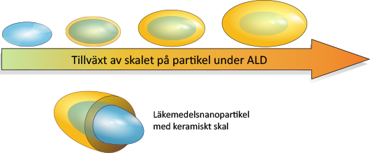
Sunday, May 31, 2015

Photoelectrochemical (PEC) water splitting technology using active ALD layers for enhanced performance

Researchers from Japan, including Fujifilm Corporation, has investigated how thin ALD NiO enhance the performance of  photoelectrochemical (PEC) devices that can be used in future water splitting plants scalable production of renewable hydrogen fuels. To do so they used a BENEQ TSF reactor for deposition of the NiOx layer. There findings were published in Journal of American Chemical Society recently online (abstract below). The conclusion was that depositing NiO on the surfaces of CoOx/BiVO4 electrodes by ALD using the Beneq TFS 200 system enhanced the performance (higher current density at lower potential) for the PEC devices.


A look inside a Beneq TFS 200 reactor (www.beneq.com)

Surface Modification of CoOx Loaded BiVO4 Photoanodes with Ultrathin p-Type NiO Layers for Improved Solar Water Oxidation

Miao Zhong, Takashi Hisatomi, Yongbo Kuang, Jiao Zhao, Min Liu, Akihide Iwase, Qingxin Jia, Hiroshi Nishiyama, Tsutomu Minegishi, Mamiko Nakabayashi, Naoya Shibata, Ryo Niishiro, Chisato Katayama, Hidetaka Shibano, Masao Katayama, Akihiko Kudo, Taro Yamada, and Kazunari Domen

J. Am. Chem. Soc., 2015, 137 (15), pp 5053–5060 DOI: 10.1021/jacs.5b00256 Publication Date (Web): March 24, 2015


Depositing NiO on the surfaces of CoOx/BiVO4electrodes by atomic layer deposition (ALD) using the Beneq TFS 200 system enhanced the performance (higher current density at lower potential) for the PEC devices.

Photoelectrochemical (PEC) devices that use semiconductors to absorb solar light for water splitting offer a promising way toward the future scalable production of renewable hydrogen fuels. However, the charge recombination in the photoanode/electrolyte (solid/liquid) junction is a major energy loss and hampers the PEC performance from being efficient. Here, we show that this problem is addressed by the conformal deposition of an ultrathin p-type NiO layer on the photoanode to create a buried p/n junction as well as to reduce the charge recombination at the surface trapping states for the enlarged surface band bending. Further, the in situ formed hydroxyl-rich and hydroxyl-ion-permeable NiOOH enables the dual catalysts of CoOx and NiOOH for the improved water oxidation activity. Compared to the CoOx loaded BiVO4(CoOx/BiVO4) photoanode, the ∼6 nm NiO deposited NiO/CoOx/BiVO4 photoanode triples the photocurrent density at 0.6 VRHE under AM 1.5G illumination and enables a 1.5% half-cell solar-to-hydrogen efficiency. Stoichiometric oxygen and hydrogen are generated with Faraday efficiency of unity over 12 h. This strategy could be applied to other narrow band gap semiconducting photoanodes toward the low-cost solar fuel generation devices.

Epitaxial growth of GaN nanowires on metallic TiN by Paul-Drude-Institut, Berlin

Paul-Drude-Institut für Festkörperelektronik in Berlin has recently published a paper (below) on how to grow GaN Nanowires on TiN. From a silicon based semiconductor device perspective this is very interesting results since TiN can be used to make ohmic contact to silicon. For instance the is used in most DRAM Capacitor cells today where the word line is connected by a TiN/Ti/TiSi/Si ohmic contact. This technology was invented by Qimonda - The buried Word Line technology that was introduced at 65 nm and has been transferred to many other companies since then (Winbond, Micron, Elpida, ...). Or as the researchers at the Paul-Drude-Institut states:  

"The freedom to employ metallic substrates for the epitaxial growth of semiconductor nanowires in high structural quality may enable novel applications that benefit from the associated high thermal and electrical conductivity as well as optical reflectivity."


Epitaxial Growth of GaN Nanowires with High Structural Perfection on a Metallic TiN Film 

M. Wölz , C. Hauswald , T. Flissikowski , T. Gotschke , S. Fernández-Garrido , O. Brandt , H. T. Grahn , L. Geelhaar *, and H. Riechert 
Nano Lett., Article ASAP DOI: 10.1021/acs.nanolett.5b00251 
Publication Date (Web): May 22, 2015


Vertical GaN nanowires are grown in a self-induced way on a sputtered Ti film by plasma-assisted molecular beam epitaxy. Both in situ electron diffraction and ex situ ellipsometry show that Ti is converted to TiN upon exposure of the surface to the N plasma. In addition, the ellipsometric data demonstrate this TiN film to be metallic. The diffraction data evidence that the GaN nanowires have a strict epitaxial relationship to this film. Photoluminescence spectroscopy of the GaN nanowires shows excitonic transitions virtually identical in spectral position, line width, and decay time to those of state-of-the-art GaN nanowires grown on Si. Therefore, the crystalline quality of the GaN nanowires grown on metallic TiN and on Si is equivalent. The freedom to employ metallic substrates for the epitaxial growth of semiconductor nanowires in high structural quality may enable novel applications that benefit from the associated high thermal and electrical conductivity as well as optical reflectivity.

ALD processing using HF to grow AlF3

Here is a interesting paper from Steven George in on growing AlF3 using HF. I haven´t seen anyone growing ALD films with HF before and usually you think of etching or surface hydrogen termination and growth passivation when HF is employed. As usual a lot of QCM growth characterization is used by the Boulder guys. The authors states that AlF3 ALD may be useful for a number of applications such as ultraviolet optical films, protective coatings for the electrodes of Li ion batteries and Lewis acid catalytic films.


Atomic Layer Deposition of AlF3 Using Trimethylaluminum and Hydrogen Fluoride 

Younghee Lee , Jaime W. DuMont , Andrew S. Cavanagh , and Steven M. George
J. Phys. Chem. C, Just
Accepted Manuscript
DOI: 10.1021/acs.jpcc.5b02625 
Publication Date (Web): May 27, 2015

The atomic layer deposition (ALD) of AlF3 was demonstrated using trimethylaluminum (TMA) and hydrogen fluoride (HF). The HF source was HF-pyridine. In situ quartz crystal microbalance (QCM), quadrupole mass spectrometer (QMS) and Fourier transform infrared (FTIR) spectroscopy measurements were used to study AlF3 ALD. The AlF3 ALD film growth was examined at temperatures from 75C to 300C. Both the TMA and HF reactions displayed self-limiting behavior. The maximum mass gain per cycle (MGPC) of 44 ng/(cm2 cycle) for AlF3 ALD occurred at 100C. The MGPC values decreased at higher temperatures. The MGPC values were negative at T> 250C when TMA and HF were able to etch the AlF3 films. Film thicknesses were also determined using ex situ X-ray reflectivity (XRR) and spectroscopic ellipsometry (SE) measurements. The AlF3 ALD growth rate determined by the ex situ analysis was 1.43 Å/cycle at 100C. These ex situ measurements were in excellent agreement with the in situ QCM measurements. FTIR analysis monitored the growth of infrared absorbance from Al-F stretching vibrations at 500-800 cm-1 during AlF3 ALD. In addition, absorption peaks were observed that were consistent with AlF(CH3)2 and HF species on the surface after the TMA and HF exposures, respectively. X-ray photoelectron spectroscopy (XPS) and Rutherford backscattering spectrometry (RBS) measurements revealed that the deposited films were nearly stoichiometric AlF3 with an oxygen impurity of only ~2 at%. AlF3 ALD may be useful for a number of applications such as ultraviolet optical films, protective coatings for the electrodes of Li ion batteries and Lewis acid catalytic films.

Saturday, May 30, 2015

Hydrophobic graphene coating could make power plants more efficient

Product Design & Development reports that a team of researchers at MIT has developed a way of coating condenser surfaces with a layer of graphene, just one atom thick, and found that this can improve the rate of heat transfer by a factor of four — and potentially even more than that, with further work. And unlike polymer coatings, the graphene coatings have proven to be highly durable in laboratory tests.


An uncoated copper condenser tube (top left) is shown next to a similar tube coated with graphene (top right). When exposed to water vapor at 100 degrees Celsius, the uncoated tube produces an inefficient water film (bottom left), while the coated shows the more desirable dropwise condensation (bottom right). Picture from www.pddnet.com - Courtesy of the researchers

The findings are reported in the journal Nano Letters by MIT graduate student Daniel Preston, professors Evelyn Wang and Jing Kong, and two others. The improvement in condenser heat transfer, which is just one step in the power-production cycle, could lead to an overall improvement in power plant efficiency of 2 to 3 percent based on figures from the Electric Power Research Institute, Preston says — enough to make a significant dent in global carbon emissions, since such plants represent the vast majority of the world’s electricity generation. “That translates into millions of dollars per power plant per year,” he explains.

Extremely thin hydrophobic coating is also obviously an open field for clever ALD solutions. Here is a recent report on conventional hydrophobic coating technologies from Vanderbilt University taking a    closer look at the US market.


The history of hydrophobic coating technologies

Thursday, May 28, 2015

Asenov claims Nanowire transistors (NWT) favourite to succeed FinFET at 5 nm

Nanowire transistors are the most likely successor to finfets and will scale to 5nm, says Professor Asen Asenov, Professor of Electrical Engineering at Glasgow University and CEO of Gold Standard Simulations (GSS) which specialises in the predictive simulation of nano-CMOS devices including statistical variability and reliability.


”While 16/14nm FinFETs are about to enter volume production at the major foundries, the next generation transistors suitable for 7nm CMOS and below are already on the drawing board,” says Asenov, “one of the best candidates “Gate all around” transistors, better known as nanowire transistors (NWT), have superior scaling properties compared to FinFETs and can be scaled to channel lengths of approximately 5nm. ”


Mobile charge distribution in a NWT with different cross-sections suitable for 7nm CMOS technology. Due to quantum mechanical confinement effects ‘strange’ patterns determine the Source' Drain' Gate' Spacer' Channel' positions of the current flow in the nanowire cross-section (Picure from GSS).

Building an advanced PEALD chamber out of a scrap AMAT P5000

Here is a story about a cool guy building advanced PEALD chamber out of a scrap AMAT P5000. I´m thinning we want to know all the details since then there are a lot of them out there to convert fro ALD! Parts of the story down here:

Lion Surplus serves as a repository for equipment, furniture and other supplies that Penn State departments no longer need. The store is open to the general public as well as the University community.


“Last spring we bought two optical tables at Surplus,” Jackson said. “They’re these big, heavy tables that have a vibration isolation system for setting up optically based experiments. One of them is now in a lab in the Millennium Science Center and it’s used as part of a project sponsored by Dow Chemical on flexible and printed electronics. The other one went to a relatively new faculty member here in electrical engineering who is starting up and growing his research program. So we got the advantage of low cost, and this repurposed equipment is serving Penn State research in an important way.”

Jackson offered an example of another valuable find: several years ago he spotted a nondescript metal box at Surplus. Recognizing the box as the chamber from an Applied Materials P5000, a commercial semiconductor process tool, he bought it at a low cost.

“My students and I used this as the starting point to build a new tool — a plasma enhanced atomic layer deposition system,” he said. “Now we have a system that allows us to do things that no expensive commercial system would. And my students’ understanding of this is far beyond what it would be if we had just bought a commercial system. The students have a sense of ownership.”

According to this publication (ZnO thin film transistors by low temperature deposition plasma-enhanced atomic layer deposition in a showerhead reactor) the AMAT P5000 PEALD reactor has the following features and capabilities after the upgrade:
  • The system is based on an Applied Materials P5000 showerhead chamber and uses a manual, single wafer, load lock. 
  • A load-locked, constant pressure, constant flow, showerhead, weak oxidant, PEALD system. 
  • A simple sample heating stage is used with either 200 mm wafers or smaller samples on aluminum 200 mm carriers. 
  • The system operates in a constant flow, constant pressure mode, with reactants and carrier gases switched in or out of the total gas flow as needed. In this mode, the sample is always exposed to gases exiting the showerhead, with little or no mixing from downstream gases. This approach also allows fast changes of reaction gas components. 
  • Typical deposition pressure is 1.5 torr and typical total flow is 1150 sccm. 
  • The volume of the region between the showerhead and substrate is about 1 liter, resulting in a gas residence time of about 100 milliseconds.

Wednesday, May 27, 2015

Swedish Nanexa demonstrate ALD controlled drug delivery

PharmaShell® is a completely new drug delivery system from Nanexa and has demonstrated great potential to revolutionize drug formulation in the future. PharmaShell® is based on containment of microscopic drug particles, which allow for new possibilities for targeting and dosing of drugs with higher precision.


Many drugs today are used as small particles and they can be administered in several ways, e.g. intravenous, orally or by inhalation. PharmaShell® provides a technique where solid drug particles in the size range of nanometers to micrometers are completely contained. The containment is provided by creating a shell, with a thickness of a few nanometers, on the surface of the drug particles. The shell is made from a mineral compound which has low solubility. This allows the shell to completely dissolve and exit the human body. The release of the contained drug is rigorously controlled by the predetermined thickness of the shell, a thicker shell takes longer time to dissolve and vice versa. In this way the extent of therapeutic time can be tailored.


Powder sample loaded into a Picosun ALD reactor.


PharmaShell® is synthesized directly on the surface of drug particles, which gives a drug load that is extremely high. The “drug load” is defined as weight of active drug in a formulation by the total weight. A high drug load in competing drug delivery systems is around 20%, with PharmaShell® the drug load is rarely below 70%.

In order to create the shell on drug particles we use a chemical deposition technique called Atomic Layer Deposition, ALD. ALD enable growth of well-controlled shells on nanoparticles in a way that no other techniques can.

A further advantage with PharmaShell® is that we provide a well-defined outer surface of the coated particles. The surface provided by PharmaShell® is covered by chemically bonded hydroxyl groups, which are most suitable for further binding of other molecules, such as targeting molecules that can otherwise be difficult to bind to surfaces of drug particles.

PharmaShell® also contributes to longer shelf life of the coated drugs. Extremely small amounts of oxygen and water can react with solid drug particles and destroy their function or merge them into larger particles. PharmaShell® is proven to be completely dense which effectively prevents oxygen, water or other gaseous compounds from penetrating and ruining the drug.

Tuesday, May 26, 2015

ALD Nano företaget Nanexa genomför nyemission inför listning


Nanexa genomför en nyemission inför noteringen på AktieTorget. Nyemissionen ska främst finansiera det fortsatta arbetet för att utveckla Bolagets innovativa drug delivery-system PharmaShell® genom att förstärka befintliga samarbeten samt utveckla nya samarbeten med ledande läkemedelsbolag.

(Information in English on PharmaShell: http://baldengineering.blogspot.fi/2015/05/swedish-nanexa-demonstrate-ald.html)

Teckningskursen är 9,00 kronor per aktie och teckningstiden löper från den 21 maj till den 5 juni 2015. Emissionen kommer vid full teckning tillföra Nanexa AB 10,4 miljoner kronor före emissionskostnader och antalet nyemitterade aktier vid full teckning uppgår till 1 150 000 stycken. Nanexa har i samband med erbjudandet erhållit teckningsförbindelser från Bolagets aktieägare Rutger Arnhult via M2 Capital Management AB och Patrik Tillman via Kattvik Financial Services AB om 1,8 mkr, motsvarande cirka 18 procent av emissionsbeloppet. Därtill har Bolaget ingått avtal om emissionsgarantier om 5,4 mkr motsvarande cirka 52 procent av emissionsbeloppet. Således är emissionen säkerställd till 70 procent. 


Bakgrund och motiv 

Nanexa utvecklar och marknadsför produkter inom nanoteknologi. Bolagets fokus ligger på PharmaShell® som är ett nytt drug delivery-system med potentialen att ge nya läkemedel specifika och avgörande egenskaper. Tekniken som använts, Atomic Layer Deposition (ALD), har av Nanexa anpassats till och utvecklats för att belägga nanometerstora läkemedelspartiklar. ALD-tekniken innebär att läkemedelspartiklar kan förses med önskat antal atomlager av en given kemisk substans, vilket skapar helt nya förutsättningar för läkemedelsformuleringar och läkemedelsutveckling. 


PharmaShell adresserar stora medicinska behov. Marknaden för nanobaserade drug delivery-system är under stark expansion och prognosticeras att växa från 30 miljarder USD 2015 till 136 miljarder USD år 2021. En viktig trend inom läkemedelsindustrin sätt att arbeta med drug delivery handlar om att styra läkemedlet till vävnad som skall behandlas och minska mängden läkemedel i övriga kroppen. På så sätt uppnås en ökad behandlingseffekt och minskade biverkningar. PharmaShell® bidrar till ökad cirkulationstid i blodbanan och ökar möjligheten att koppla målstyrningsmolekyler till skalet som binder mot endast en typ av vävnad, exempelvis en tumör eller specifika platser i hjärtat eller andra organ. I maj 2013 ingicks ett samarbete med AstraZeneca kring utvecklingen av PharmaShell®. Avtalet med AstraZeneca är ett så kallat ”Material Transfer and Feasibility Study Agreement”. 

Emissionskapitalet ska användas till att ta produkten PharmaShell® från så kallat proof of concept till validerad produkt, samt till investeringar i övrig produktportfölj, immateriella rättigheter, marknadsföring samt rörelsekapital. 

Kolla in här för mer information:

MISOKA - The Nano CMP tooth brush from Japan

MISOKA - A new tooth brush from Japan uses nanotechnology to clean your teeth without the use of tooth paste. To me this seems to be pretty advanced technology from Chemical Mechanical Polishing (CMP) used in the semiconductor industry to planarize interconnects. All information below from the company webpage (http://www.misoka.jp/salone2015/salone2015-en.html).


Simply moisten the bristles and brush your teeth. The MISOKA toothbrush cleans your teeth by using the action of nano-sized mineral particles on the bristles to remove plaque from the surfaces of your teeth. It also gives the surfaces a smoother feel by making them more hydrophilic. This ground-breaking new toothbrush gives you the confidence of knowing you have brushed your teeth properly, leaving the inside of your mouth feeling fresher by making it more difficult for plaque and other material to stick to your teeth. So long as you don’t brush so hard that it hurts your gums, each MISOKA toothbrush will last for about one month.


  • Nano-sized mineral ions on the brush bristles help clean plaque from the teeth.
  • Brushing leaves an ion coating on the surface of the teeth that makes it more difficult for plaque and other material to adhere.
This picture looks a bit like an ALE process... The Atomic Layer Brush :-)

And yes you can buy it on Amazon for 14 US Dollar and until now over 2 million has been sold. 

MISOKA Toothbrush


Price:$14.12 FREE Shipping
In stock.
Ships from and sold by K-I-M-JAPAN.
    Estimated Delivery Date: June 1 - 4 when you choose Expedited at checkout.
    • Size (about): [package] width 20 × 4.5 × height back 2cm, 1cm length of [body] pattern 18.5 × 1.3cm hair
    • Material: [pattern] AS resin, [hair] nylon
    • Normal: Hardness of the hair


    Monday, May 25, 2015

    China's nano composite zirconia market capacity approximated at 7,000 tons in 2014

    For those of you ALD guys devoted to high-k this might be interesting facts. As reported by AZONano recently: Nano Zirconia, with zirconium dioxide as key ingredient, constitutes nano composite zirconia after being added with rare-earth elements (primarily yttrium oxide) and other oxides. Nano composite zirconia gets widely used in fields like grinding materials, coating, fuel cell, artificial teeth, automobile exhaust catalyst promoter, etc.

    As its industrialization is under way for just three decades, nano composite zirconia's applications in only grinding media and oxygen sensor have become mature, while other applicable areas are experiencing a fast growing period and even at the initial stage. 
    • In 2014, the global sales volume of nano composite zirconia totaled roughly 40,000 tons, which generated revenue of RMB14 billion. 
    • China's nano composite zirconia market capacity approximated 7,000 tons.

    Globally, the nano composite zirconia capacity spreads mainly in Europe and Japan, with the companies with complete industrial layout including Saint-Gobain, Tosoh, and DKKK. In addition, the players like Showa Denko, Solvay, and Sumitomo Osaka Cement occupy an important position in some market segments.

    Domestically, only Sinocera and Jiujiujiu were the first to make technological breakthroughs and began pilot production. Sinocera's scale of pilot production totaled 200t/a. In the first half of 2014, its nano composite zirconia segment contributed revenue of RMB4.809 million, versus the operating cost of RMB2.961 million. Additionally, the company announced a 1,500 t/a expansion plan, according to which the products (700 tons) from the first phase of the project would be very likely released in the second quarter of 2015.

    Jiujiujiu has developed the about 10nm, 20nm, 40nm, and 80nm series of nano composite zirconium dioxide powder. At present, the company's pilot project is in trial production.

    Continued support for molecules which function like machines with another 8.9 million EUR

    Nanotechnology project on molecular machines receives its third round of funding (Nanowerk News) Great excitement at Kiel University: As the DFG (German Research Foundation) announced it will continue to support the research on molecules which function like machines with another 8.9 million EUR. 


    This funding will allow the scientists in Germany's northernmost state to develop new engineering techniques for building tiny machine-like molecules over the next four years. The ultimate miniaturisation of engineering functions should improve the efficiency of energy conversion systems, medicines, diagnostic methods and materials. Moreover, completely new areas of applications will open up along this line. 

    The Collaborative Research Centre 677 (SFB 677) "Function by Switching" now starts into the third and final funding period. Collaborative Research Centres are supported for a maximum of twelve years. They are highly competitive and prestigious flagship institutions at German universities. In total, around 100 scientists from the fields of chemistry, physics, material sciences and medicine collaborate in this Kiel based research network. 


    Subproject Overview

    Project Area A

    First and foremost, we will synthesize the elementary molecular switches as well as their neighboring environment (supramolecular aggregates) in homogeneous solution using classical methods of synthetic chemistry. Elemental processes, e.g. the switching process and its mechanism, will also be investigated in solution first, as there are efficient analytical methods available for this environment. We will benefit from these results to establish and optimize the application of the molecules on surfaces (project area B) and in functional materials (project area C).
    show list of projects in area A

    Project Area B

    Arranging and operating switching molecules on surfaces comprises the subprojects in area B. The alignment of the switches on the surface, i.e. distance and orientation of the switches with respect to the surface as well as to each other, is an essential requirement to achieve a programed function. Scanning tunneling microscopy and spectroscopy are availabe to characterize surfaces. Various efficient surface sensitive techniques will be used to to confirm the switching process and the triggered function.
    show list of projects in area B

    Project Area C

    The incorporation of molecular switches into functional materials such as coordination polymers, pores or nanocomposites facilitates the switching of properties such as conductivity, refraction, diffusion or adsorption. Target applications include switchable storage media as well as optical and molecular filters.
    show list of projects in area C

    Project Area Z

    Project area Z contains the collaborative research center's central projects, i.e. the research training group as well as public relations.
    show list of projects in area Z


    The 20 Biggest ALD Customers 1Q / 2015

    Here it is the biggest ALD Customers 1Q / 2015 :-)


    The first Russian PEALD Sytem presented at VacuumTechExpo2015 in Russia

    Research Institute of Precise Machine Manufactory has been awarded for ALD coating unit at VacuumTechExpo2015. This is first R&D PEALD system designed and manufactured in Russia. The company locates in Zelenograd, Moscow.


    The new ALD coating unit with remote inductively coupled plasma source and heated substrate holder.


    Research Institute of Precision Machine Manufacturing (NIITM) was established in 1962 in Zelenograd to become a key enterprise with the main focus on creation of specific processing equipment for electronic industry. Equipment based on NIITM development formed the foundation of semiconductor production in Russia and Soviet republics.


    Equipment of the company was exported to the CMEA countries and China. Nowadays Research Institute of Precision Machine Manufacturing belongs to a group of companies "Micron" - the largest producer and exporter of integrated circuits in Russia and the CIS countries.

    Research and production activities of NIITM are marked by a variety of fundamental and applied researches and developments: a number of scientific works are published; more than 600 certificates for the invention and patents are received.


    Innovative projects of the company are awarded by state decorations, Orders and Medals at international exhibitions.

    NIITM offers services for development of a wide range of research and industrial technological equipment and supplies vacuum-plasma and physical and thermal chambers as well as clusters based on it for process implementation in nano-, micro- and electronics, medicine, solar energy, etc.

    Sunday, May 24, 2015

    ALD tantalum oxide in a passivation stack for silicon solar cells

    This is an interesting paper on Ta2O5 ALD for surface passivation in silicon based solar cells. As the authors point out, despite more than four decades of work on Ta2O5, no attempt has yet been made to study this material on c-Si as an electronic passivating layer. Ta2O5 has excellent optical properties:

    • a relatively high refractive index 
    • a negligible absorption in the visible range

    This is why Ta2O5 is often used as antireflection coating (ARC). The work below by researchers at The Australian National University in Canberra was performed in a Picosun R200 Advanced ALD reactor using Tantalum Ethoxide as tantalum precursor and H2O as the oxidant at 250 °C. The reactor is located at the Australian National Fabrication Facility (ANFF).


    Established under the National Collaborative Research Infrastructure Strategy, the Australian National Fabrication Facility (ANFF) links 8 university-based nodes to provide researchers and industry with access to state-of-the-art fabrication facilities (http://www.anff.org.au).

    Tantalum oxide/silicon nitride: A negatively charged surface passivation stack for silicon solar cells (Open Access)

    Yimao Wan, James Bullock and Andres Cuevas
    Appl. Phys. Lett. 106, 201601 (2015); http://dx.doi.org/10.1063/1.4921416 

    This letter reports effective passivation of crystalline silicon (c-Si) surfaces by thermal atomic layerdeposited tantalum oxide (Ta2O5) underneath plasma enhanced chemical vapour depositedsilicon nitride (SiNx). Cross-sectional transmission electron microscopy imaging shows an approximately 2 nm thick interfacial layer between Ta 2O5 and c-Si. Surface recombination velocities as low as 5.0 cm/s and 3.2 cm/s are attained on p-type 0.8 Ω·cm and n-type 1.0 Ω·cm c-Si wafers, respectively. Recombination current densities of 25 fA/cm2 and 68 fA/cm2 are measured on 150 Ω/sq boron-diffused p + and 120 Ω/sq phosphorus-diffused n + c-Si, respectively. Capacitance–voltage measurements reveal a negative fixed insulator charge densityof −1.8 × 1012 cm−2 for the Ta 2O5 film and −1.0 × 1012 cm−2 for the Ta 2O5/SiNx stack. The Ta2O5/SiNx stack is demonstrated to be an excellent candidate for surface passivation of high efficiency silicon solar cells.

    Next-Generation Lithium Metal Anode Engineering by Atomic Layer Deposition

    Researchers at University of Maryland demonstrate Al2O3 ALD of protection layers directly on Li metal that protect the Li surface from corrosion due to atmosphere, sulfur, and electrolyte exposure. Lithium metal is considered to be the most promising anode for next-generation batteries due to its high energy density of 3840 mAh g–1. Major obstacles for lithium metal anodes is that the Li surface is highly reactive which can lead to reactions with the solvents and the electrolyte and contamination, reducing the performance of batteries employing Li metal anodes. 

    Next-Generation Lithium Metal Anode Engineering via Atomic Layer Deposition 

    Alexander C. Kozen, Chuan-Fu Lin, Alexander J. Pearse, Marshall A. Schroeder, Xiaogang Han, Liangbing Hu, Sang-Bok Lee, Gary W. Rubloff, and Malachi Noked


    Lithium metal is considered to be the most promising anode for next-generation batteries due to its high energy density of 3840 mAh g–1. However, the extreme reactivity of the Li surface can induce parasitic reactions with solvents, contamination, and shuttled active species in the electrolyte, reducing the performance of batteries employing Li metal anodes. One promising solution to this issue is application of thin chemical protection layers to the Li metal surface. Using a custom-made ultrahigh vacuum integrated deposition and characterization system, we demonstrate atomic layer deposition (ALD) of protection layers directly on Li metal with exquisite thickness control. We demonstrate as a proof-of-concept that a 14 nm thick ALD Al2O3 layer can protect the Li surface from corrosion due to atmosphere, sulfur, and electrolyte exposure. Using Li–S battery cells as a test system, we demonstrate an improved capacity retention using ALD-protected anodes over cells assembled with bare Li metal anodes for up to 100 cycles.

    Atomic Layer CVD of WSe2 with Tunable Device Characteristics

    Viterbi School Of Engineering, University of Southern California report on ambient pressure chemical vapor deposition (CVD) growth of monolayer and few layer WSe2 flakes directly on silica substrates. This study is of high interest for future 2D material based transistors and optoelectronic devices.


    Chemical Vapor Deposition Growth of Monolayer WSe2 with Tunable Device Characteristics and Growth Mechanism Study 

    Bilu Liu, Mohammad Fathi , Liang Chen , Ahmad Abbas , Yuqiang Ma , and Chongwu Zhou
    ACS Nano, Article ASAPDOI: 10.1021/acsnano.5b01301Publication Date (Web): May 22, 2015


    Semiconducting transition metal dichalcogenides (TMDCs) have attracted a lot of attention recently, because of their interesting electronic, optical, and mechanical properties. Among large numbers of TMDCs, monolayer of tungsten diselenides (WSe2) is of particular interest since it possesses a direct band gap and tunable charge transport behaviors, which make it suitable for a variety of electronic and optoelectronic applications. Direct synthesis of large domains of monolayer WSe2 and their growth mechanism studies are important steps toward applications of WSe2. Here, we report systematical studies on ambient pressure chemical vapor deposition (CVD) growth of monolayer and few layer WSe2 flakes directly on silica substrates. The WSe2 flakes were characterized using optical microscopy, atomic force microscopy, Raman spectroscopy, and photoluminescence spectroscopy. We investigated how growth parameters, with emphases on growth temperatures and durations, affect the sizes, layer numbers, and shapes of as-grown WSe2 flakes. We also demonstrated that transport properties of CVD-grown monolayer WSe2, similar to mechanically exfoliated samples, can be tuned into either p-type or ambipolar electrical behavior, depending on the types of metal contacts. These results deepen our understandings on the vapor phase growth mechanism of WSe2, and may benefit the uses of these CVD-grown monolayer materials in electronic and optoelectronics.

    Friday, May 22, 2015

    Imec 5 day training in Nanoscale CMOS process technology


    Imec offers a 5 day training in Nanoscale CMOS process technology 8-12 June in Leuven, Belgium. Here is the full program and for ALD guys there is especially two sessions that must be of interest (below) plus courses  in interconnects, memory and emerging memory.


    Material deposition 

    Essentially, manufacturing of semiconductor devices is based on the deposition and removal of layers/materials, with intermediate lithographic patterning steps. This lecture gives an overview of the most prevalent layer deposition processes as used in manufacturing of semiconductor circuits. Basically, most of these processes are based on the use of chemical precursors and are therefore called ‘Chemical Vapor Deposition’ processes. Next to the generic thermal and plasma-enhanced CVD processes, there are more specific types of CVD processes such as epitaxy used for the growth of mono-crystalline semiconductor layer structures and Atomic Layer Deposition (ALD) used for the deposition of various materials. A powerful technique based on atomic precursors (Physical Vapor Deposition, PVD) is Molecular Beam Epitaxy, which is mainly used in R&D due to its high flexibility.

    By Roger Loo 

    Gate stack 

    The properties of silicon dioxide are seen as key to the success of the CMOS indus- try due to the high electrical quality of the Si/SiO2 interface, its favorable material properties and reliability. The continued reduction of the physical oxide thickness demanded by the scaling requirements ultimately renders the material unfit for further scaling as it would increase the gate leakage current prohibitively due to fundamental quantum mechanical tunneling. Materials with a higher dielectric con- stant (k-value) maintain channel control for larger thicknesses and reduce the gate leakage current. The introduction of high-k metal gate technology, which resolved the gate leakage issue in 45 nm production MOSFETs is one of the largest recent innovations in CMOS technology. This lecture discusses the properties of SiO2 lay- ers and introduces the high-k and metal gate technology used for advanced CMOS devices. 

    By Lars-Ake Ragnarsson

    Phosphorene transistors and circuit units for flexible Nanoelectronics

    Phosphorene transistors and circuit units feature outstanding electrical performance and strong mechanical robustness and can therefore be used in flexible nanoelectronics for building transistors and other devices. Here is a good paper in SPIE Newsroom from University of Texas at Austin

    Phosphorene for flexible nanoelectronics

    Weinan Zhu, Maruthi N. Yogeesh and Deji Akinwande


    Few-layer black phosphorus (BP) has attracted ever more attention since its debut last year as a new 2D layered semiconductor.1, 2 The puckered crystal structure distinguishes its physical properties from plane-structured graphene with a thickness-tuned bandgap ranging from 0.3 to ∼2eV. Its exceptional electrical properties include high hole mobility (∼1000 cm2/Vs) and high field-effect current modulation (105).2, 3 These properties enable both high-speed and low-power nanoelectronic applications beyond the demonstrated performance capability of graphene or transitional metal dichalcogenides (TMDs).

    Intel invests in ALD Precursor Company Digital Specialty Chemicals Limited (DSC)

    Digital Specialty Chemicals Limited (DSC), a dual bottom line corporation and leading provider of advanced materials to the semiconductor, pharmaceutical, and specialty chemical markets, announced today that it has received an equity investment from Intel Capital, Intel Corporation’s global investment organization. The investment will enhance the company’s research and development capabilities and will accelerate manufacturing capacity expansion.


    DSC specializes in the manufacture of organophosphorus and organometallic chemistries used in both memory and logic thin film atomic layer deposition (ALD) manufacturing processes at leading semiconductor integrated circuit (IC) fabrication sites worldwide. The company is a leader in the manufacturing and handling of both novel specialty chemicals in large volume, high purity air- sensitive chemicals that require nitrogen and vacuum-operated vessels, using high pressure reactors and multiple distillation techniques.


    “Since 1987, we have provided custom and high volume high purity chemicals to the semiconductor, pharmaceutical and specialty chemical markets worldwide. Our people, processes and facilities combine to offer the agility of a small, fine- chemical operation with the capacity of a large supplier,” said Dr. Ravi R. Gukathasan, CEO. “We believe that the continuation of Moore’s Law for semiconductor processing will depend greatly on continued innovation of advanced precursors which provides a growth opportunity for DSC. The funding from Intel Capital will help enable us to construct state-of-the-art R&D and manufacturing facilities to meet growing demand for thin film technologies.”

    “Materials innovation is critical to enabling new capabilities in semiconductor device design and manufacturing,” said Robert Bruck, corporate vice president and general manager of Global Supply Management at Intel. “We look forward to supporting DSC’s growth including development of new materials technologies for advanced semiconductor manufacturing process technology nodes.”

    Thursday, May 21, 2015

    Flash-Enhanced Atomic Layer Deposition

    Here is a recent review from ALD Lab Dresden - IHM, TU Dresden on Flash-Enhanced Atomic Layer Deposition (FEALD) with Open Access. The paper was presented at the Cancun, Mexico, Meeting of the Society, October 5–9, 2014. Thanks Henrik Pedersen for sharing this one!


    The basic principle of Flash-Enhanced Atomic Layer Deposition according to ALD Lab Dresden.


    Flash-Enhanced Atomic Layer Deposition: Basics, Opportunities, Review, and Principal Studies on the Flash-Enhanced Growth of Thin Films (Open Access)

    Thomas Henke, Martin Knaut, Christoph Hossbach, Marion Geidel, Lars Rebohle, Matthias Albert, Wolfgang Skorupa and Johann W. Bartha

    This was Paper 1616 presented at the Cancun, Mexico, Meeting of the Society, October 5–9, 2014.


    Within this work, flash lamp annealing (FLA) is utilized to thermally enhance the film growth in atomic layer deposition (ALD). First, the basic principles of this flash-enhanced ALD (FEALD) are presented in detail, the technology is reviewed and classified. Thereafter, results of our studies on the FEALD of aluminum-based and ruthenium thin films are presented. These depositions were realized by periodically flashing on a substrate during the precursor exposure. In both cases, the film growth is induced by the flash heating and the processes exhibit typical ALD characteristics such as layer-by-layer growth and growth rates smaller than one Å/cycle. The obtained relations between process parameters and film growth parameters are discussed with the main focus on the impact of the FLA-caused temperature profile on the film growth. Similar, substrate-dependent growth rates are attributed to the different optical characteristics of the applied substrates. Regarding the ruthenium deposition, a single-source process was realized. It was also successfully applied to significantly enhance the nucleation behavior in order to overcome substrate-inhibited film growth. Besides, this work addresses technical challenges for the practical realization of this film deposition method and demonstrates the potential of this technology to extend the capabilities of thermal ALD.


    Wednesday, May 20, 2015

    Imec and Tokyo Electron Demonstrate Direct Cu Etch Scheme for Advanced Interconnects

    IEEE IITC, Grenoble, (France) – May 20, 2015 – As reported by Imec. Today, at the IEEE IITC conference, nano-electronics research center imec and Tokyo Electron Limited (TEL) presented a direct Cu etch scheme for patterning Cu interconnects. The new scheme has great potential to overcome resistivity and reliability issues that occur while scaling conventional Cu damascene interconnects for advanced nodes.


    TEM section of copper etched lines encapsulated by SiN cap layer (Imec news).

    Aggressive scaling of damascene Cu interconnects leads to a drastic increase in the resistivity of the Cu wires, due to the fact that grain size is limited by the damascene trenches, which results in increased grain boundary and surface scattering. Additionally, the grain boundary negatively influences electromigration. When scaling damascene Cu interconnects, reliability issues occur because the overall copper volume is reduced and interfaces become dominant. Imec and TEL have demonstrated the feasibility of a direct Cu etch scheme to replace the conventional Cu damascene process. A key advantage of the direct Cu etch process is that it systematically results in larger grain sizes. Moreover, electromigration performance is preserved by applying an in-situ SiN cap layer that protects the Cu wires from oxidation and serves as the Cu interface.

    The results were achieved in cooperation with imec’s key partners in its core CMOS programs GLOBALFOUNDRIES, Inc., Intel Corp, Micron Technology, Inc., Panasonic Corporation, Samsung Electronics Co., Ltd.,, Taiwan Semiconductor Manufacturing Co., Ltd., SK hynix Inc., Fujitsu Semiconductor Ltd., and Sony Corporation.


    Tuesday, May 19, 2015

    Picodeon PLD technology enables microstructural control

    Finnish thin film coating specialist Picodeon Ltd Oy has developed* its ultra-short pulsed laser deposition (USPLD) surface coating technology to be able to create either porous or dense aluminium oxide (Al2O3) coatings on heat-sensitive substrates for use in a wide range of industrial metallisation applications. Porous Al2O3 layers are used for instance as filters and electrical insulation layers. Dense Al2O3 is used as a barrier layer and is also an excellent optical coating with high transmittance properties. The Picodeon process enables precise micro-structural control of Al2O3 coatings, and therefore coating characteristics, by the simple management and maintenance of coating process parameters on Coldab® Series4 USPLD batch process coating equipment. 


    "This development has enormous potential for new applications of dense and porous aluminium oxide coatings on heat sensitive materials," said Picodeon VP Sales and Business Development Marko Mylläri. "It is currently very difficult to achieve these results using physical vapour deposition (PVD), sputtering or chemical vapour deposition (CVD) surface coating technologies." 

    The Coldab® Series4 equipment has built-in online plasma monitoring and laser power measurement that enable very precise management of coating process parameters, as well as a PC controlled automation that records the actions of the coating process. The metrics provided by these systems mean that the coating process, and especially the thin film quality, can be controlled with great accuracy to achieve coating characteristics within highly targeted parameters. Test production runs, for example, showed that the system could improve the porosity of a 3µm Al2O3 coating, for example, from 10 percent to as much as 45 percent by tuning the scanning speed and laser power repetition rate.

    The Al2O3 coatings were applied on heat-sensitive polyethylene (PE) and thermoplastic polyurethane (TPU) polymer film substrates. This is possible due to the low process temperatures required for surface coating using Picodeon's Coldab® USPLD system - one of the major benefits of the process.

    In addition to Al2O3, the new Picodeon process technology can be used for other coatings as well. Picodeon has produced metallic coatings using Au and Cu, and oxides such as TiO2. Picodeon's recently released ColdAb Series4 equipment is currently being installed in commercial applications, and the company is continuing development to industrialise its USPLD processes and tools towards even larger scale volume production capabilities.


    *As far as I know this product comes out of a joint development with PVD Products as stated in earlier    Press releases :

    http://www.pvdproducts.com/news/pvd-products-to-build-coldab-series-4-system-for-picodeon-ltd-2

    Imec and Lam Research Corporation Develop Novel ELD Metallization

    New Approach to Pave the Way for Advanced Interconnects Enabling Future Technology Nodes

    IEEE IITC, Grenoble (France)—May 19, 2015— During the IEEE IITC conference in Grenoble, the nanoelectronics research center imec and Lam Research Corporation today presented a novel bottom-up prefill technique for vias and contacts. The technique, based on Electroless Deposition (ELD)* of Cobalt (Co) is a highly selective method resulting in void-free filling of via and contact holes. Potentially increasing the circuit performance, it is a promising path to scaling advanced interconnects and enabling future logic and DRAM nodes at the 7 nm node and below.


    Co ELD on Palladium/Tungsten (Pd/W) for different timed stops to yield an (i) under fill, (ii) potential ideal stop or an (iii) overburden in 28nm holes (Aspect Ratio (AR) 4.5).

    As logic and memory nodes scale, performance of these advanced interconnects is negatively impacted by increasing interconnect resistance. Furthermore, voids that occur in heavily scaled vias severely impact yield. Imec’s industrial affiliation program on advanced interconnects is exploring novel metallization methods to solve these issues. One way to solve the problem is to identify integration and metallization alternatives that provide resistance benefits over conventional technology without compromising reliability and yield. Together with Lam Research, a Co ELD technique was demonstrated as a feasible method for highly selective bottom-up contact fill and via prefill with Cobalt (Co) as an alternative metal to Copper (Cu). Moreover, the high selectivity of the ELD process, at lower cost compared to Chemical Vapor Deposition (CVD), intrinsically ensures a good metal-to-metal interface and paves the way to void-free via filling and increased yield. Trench fill yield and line resistance may also benefit from the de-coupling of line and via aspect ratios, permitting the design of each for optimum Resistance/Capacitance (RC). Therefore, Co prefill ELD has the potential to enable future scaling of advanced logic and memory technologies.

    The results were achieved in cooperation with imec’s key partners as part of its core CMOS programs: GlobalFoundries, Intel, Samsung, SK hynix, Sony, TSMC, Amkor, Micron, Utac, Qualcomm, Altera, Fujitsu, Panasonic, and Xilinx.

    * ELD means fire in Swedish, how did I not see this one coming... All these wasted years with ALD... 

    Monday, May 18, 2015

    ALD boosts efficiency to 22.1% for nano structured Black Silicon solar cells

    As reported by The researchers from Finland's Aalto University and Universitat Politècnica de Catalunya have obtained the record-breaking efficiency of 22.1% on nanostructured silicon solar cells as certified by Fraunhofer ISE CalLab. 

    An almost 4% absolute increase to their previous record is achieved by applying a thin passivating film on the nanostructures by Atomic Layer Deposition, and by integrating all metal contacts on the back side of the cell.


    The surface area of the best cells in the study was already 9 cm2. This is a good starting point for upscaling the results to full wafers and all the way to the industrial scale (Aalto University).


    The results were published online 18.5.2015 in Nature Nanotechnology.

    Black silicon solar cells with interdigitated back-contacts achieve 22.1% efficiency

    Hele Savin, Päivikki Repo, Guillaume von Gastrow, Pablo Ortega, Eric Calle, Moises Garín
    & Ramon Alcubilla

    Nature Nanotechnology (2015) doi:10.1038/nnano.2015.89


    Figure 1: Structure and reflectance of b-Si. a, Scanning electron microscopy (SEM) image (cross-sectional view) of a b-Si surface. Typical height of a silicon pillar, ∼800 nm; diameter at the bottom of the pillar, ∼200 nm. The 20 nm Al2O3 layer can be seen as a brighter layer on t…

    The nanostructuring of silicon surfaces—known as black silicon—is a promising approach to eliminate front-surface reflection in photovoltaic devices without the need for a conventional antireflection coating. This might lead to both an increase in efficiency and a reduction in the manufacturing costs of solar cells. However, all previous attempts to integrate black silicon into solar cells have resulted in cell efficiencies well below 20% due to the increased charge carrier recombination at the nanostructured surface. Here, we show that a conformal alumina film can solve the issue of surface recombination in black silicon solar cells by providing excellent chemical and electrical passivation. We demonstrate that efficiencies above 22% can be reached, even in thick interdigitated back-contacted cells, where carrier transport is very sensitive to front surface passivation. This means that the surface recombination issue has truly been solved and black silicon solar cells have real potential for industrial production. Furthermore, we show that the use of black silicon can result in a 3% increase in daily energy production when compared with a reference cell with the same efficiency, due to its better angular acceptance.

    Sunday, May 17, 2015

    2016 will be another growth year for OEM stocks and Atomic Layer Processing

    2016 will be another growth year for OEM stocks and Atomic Layer Processing. In a report recently published by JP Morgan, analysts predicted another growth year in 2016 for Semiconductors stocks, driven by technology transitions in memory and 10nm FinFET. So this is good news for all Tier 1 OEMs with a number of ALD and ALE technologies in the game.

    Technology transitions by memory companies :
    • continued 3D NAND ramps
    • additional 20nm conversions
    • initial 1Xnm DRAM deployments
    Foundry and logic companies :
    • deploying FinFET technologies (especially 10nm FinFET) 
    • multi-patterning steps and vertical transistors
    "In general, we see capital intensity increasing by 10-15% on a per wafer basis when transitioning from 14nm/16nm FinFET to 10nm FF and by 15+% when transitioning to 20nm and below DRAM / 3D NAND. The number of critical patterning layers is increasing dramatically – in the foundry/logic segment, the number of critical layers is increasing by over 3x going from 28 nm node to the 10nm node…a significant increase," the analysts added.
    Read more: http://www.benzinga.com/analyst-ratings/analyst-color/15/05/5488523/jp-morgan-sees-another-growth-year-for-semiconductors-th#ixzz3aNRgk5q0

    Below is an overview of some of the ALD and ALE technologies offered by the leading OEMs. It is ion sense complete yet so please let me know what is missing (jonas.sundqvist@baldengineering.com).

    LAM Research


    LAM Research reported in 2014 that "The latest in Lam's market-leading tungsten deposition product line, the ALTUS Max ICEFill system controls variability by providing void-free fill of the geometrically complex 3D NAND wordlines. Using a proprietary filling technique, the new system creates the tungsten wordlines with an inside-out atomic layer deposition (ALD) process. The ICEFill process completely fills the lateral (horizontal) lines without any voids, while at the same time minimizing deposition in the vertical channel area. As a result, both electrical performance and yield are enhanced."


    Lam’s ALTUS systems combine CVD and ALD technologies to deposit the highly conformal films needed for advanced tungsten metallization applications (http://www.lamresearch.com/products/deposition-products).

    Lam's new ALE capability on the 2300 Kiyo F Series conductor etch system provides both the productivity and technology needed. The product leverages fast gas switching and advanced plasma techniques in the reactor to boost throughput, while dynamic RF bias enables the directional etching required to remove material in high aspect ratio (deep and narrow) features. As the latest offering in Lam's market-leading Kiyo family, the 2300 Kiyo F Series system continues to provide superior uniformity and repeatability enabled by a symmetrical chamber design, advanced electrostatic chuck technology, and independent process tuning features.


    • Shallow trench isolation
    • Source/drain engineering
    • High-k/metal gate
    • FinFET and tri-gate
    • Double and quadruple patterning
    • 3D NAND

    To learn how atomic layer deposition (ALD) and atomic layer etch (ALE) processes work, watch this video from LAM Research (www.youtube.com).

    Applied Materials

    CENTURA® ISPRINT™ TUNGSTEN ALD/CVD - The Applied Centura iSprint Tungsten ALD/CVD system provides complete contact/via fill for structures with aspect ratios ranging from 4:1 to 7:1 and extends the capability of tungsten technology to 20nm/16nm for logic and memory applications.


    The iSprint system also delivers high throughput and low cost of consumables with an optimized ALD chamber design featuring a proprietary rapid gas delivery system and small chamber volume that enable fast, effective gas purging that uses less gas (www.appliedmaterials.com).

    CENTURA® INTEGRATED GATE STACKThe system consists of an ALD HfO2 (hafnium oxide) deposition chamber and specialized chambers for interface layer oxide formation, post high-k nitridation, and post-nitridation anneal


    The Centura Integrated Gate Stack system with ALD high-k chamber technology for 22nm and below uses Applied’s production-proven Centura Gate Stack platform to deliver the complete high-k process sequence in a controlled high vacuum environment without an “air break” (www.appliedmaterials.com).


    Steven Hung, Ph.D. who specializes in integrating ALD into the transistor manufacturing process, dives deep into the chip to show what tomorrow's transistors look like, how they work, and how Applied can help the industry meet the challenges of fabricating these ultra-tiny structures to make faster, more power-efficient microchips 
    (www.youtube.com).

    Tokyo Electron

    Tokyo electron has a number of ALD technologies and are very strong in batch processing that is used to large extent in DRAM production to get the cost per wafer down since DRAM is a commodity product.
    • TEL Formula - Mini batch, thermal processes including ALD for High-k, SiO2, SiN.
    • TEL INDY Plus - Large batch, thermal processes including ALD for High-k, SiO2, SiN.
    • TEL INDY IRad - Large batch, PEALD for ultra low temperature SiO2 and SiN.
    • TEL NT333 - Single wafer cluster tool for high t-put SiO2.

    TEL INDY Large batch furnace for thermal processing and ALD (www.tel.com)


    The NT333 applies inherent ALD concepts against conventional ALD processing to address the critical performance needs imposed by aggressive geometries. The NT333 can effectively deposit with a very tight thickness control, a range of less than 1A, while maintaining a productivity of 100+ wafers per hour. With a very unique reactor design, each of the ALD duty cycles enables the NT333 to deliver the high film quality which is typically compromised at low temperature regimes (<400C). (www.tel.com)

    ASM International

    ASM's ALD technologies, includes thermal ALD (Pulsar) for FinFET high-k metal gate stacks, and various applications of Plasma Enhanced ALD (Emerald) as an enabler for low temperature processing such as multiple patterning on resist and deposition of doped silicon oxide for solid state doping of FinFETs.


    ASM’s Pulsar uses ALD to deposit the high-k dielectric materials required for advanced CMOS transistor gates ​and other applications. Pulsar is the benchmark ALD high-k tool for the industry. It was the first ALD system to be used for high-volume production at advanced customers for high-k metal gate transistors (www.asm.com).


    EmerALD XP is a process module designed to deposit thin conformal metal and dielectric ​layers by atomic layer deposition (ALD) used for advanced CMOS gate stacks and other applications (www.asm.com).


    ​​​Eagle XP8 is a high productivity 300mm tool for PEALD applications. The Eagle XP8 PEALD system can be configured with up to four Dual Chamber Modules (DCM), enabling eight chambers in high volume production within a very compact footprint (www.asm.com).


    ASM Chip Making Process (www.youtube.com)