#ALDep TiO2 #Photocatalysis DESI-MS Rotating Array Platform for High-Throughput Investigation of Oxidation Reactions https://t.co/ELT4BEixd8— Ville Miikkulainen (@vmiikkulainen) October 29, 2017
Header


%20(1).png)
Monday, October 30, 2017
New high-throughput platform for studying TiO2 photocatalytic oxidation reactions
Researches from University of Helsinki present a new high-throughput platform for studying titanium dioxide (TiO2) photocatalytic oxidation reactions.
Wednesday, October 25, 2017
Aixtron's sale of ALD/CVD Product Line to Eugene Technology in South Korea gets US approval
Aixtron SE (AIXG), announced Tuesday
that the Committee on Foreign Investment in the United States or CFIUS
has approved the sale of ALD and CVD memory product line.

Eugene
Technology CEO Eom Pyeong-yong (left) and Aixtron CEO Kim Schindelhauer
pose for a photo holding their contract. (Picture credit: Pulse by
Maeil Business Newspaper & mk.co.kr LINK)
The
company noted that the investigation by the CFIUS of the sale of
AIXTRON's ALD and CVD memory product line to Eugene Technology in South
Korea resulted in a determination that there are no unresolved U.S.
national security concerns from CFIUS' perspective.
Tuesday, October 24, 2017
Picosun’s ALD technology improves lifetime and reliability of electronic circuit boards
ESPOO, Finland, 24th October, 2017 – Picosun Oy, leading provider of advanced Atomic Layer Deposition (ALD) solutions for global industries, has invented an ALD-based method(*) with which the operational lifetime and reliability of printed circuit board assemblies (PCBA) can be efficiently improved.
Metal whisker formation and corrosion are some key factors that cause PCBA performance degradation over time. Metal whiskers are thin filaments or threads growing out from solders, components, and interconnects on the PCBA, and they can cause short-circuiting that leads to a system failure. This is particularly fatal in several sensitive applications such as medical, automotive, space, aviation, military, and industrial control electronics.
Metal whisker formation and corrosion are some key factors that cause PCBA performance degradation over time. Metal whiskers are thin filaments or threads growing out from solders, components, and interconnects on the PCBA, and they can cause short-circuiting that leads to a system failure. This is particularly fatal in several sensitive applications such as medical, automotive, space, aviation, military, and industrial control electronics.

Previously, lead has been added to solder alloys to prevent whisker formation, but the current environmental regulations prohibit its use. This is why novel methods, such as the ALD-based surface protection technique developed and now industrially enabled by Picosun are very much sought after amongst the electronics manufacturers. In Picosun’s approach, application-specifically tailored ALD nanolaminate forms a dense, conformal, and hermetic seal on the PCBA. This seal protects the PCBA components from the corrosion caused by moisture and impurities in the ambient air and blocks the metal whisker propagation. As ultra-thin films, ALD coatings have the additional benefit of allowing postprocessing of the PCBA, and they do not increase its mass or dimensions. Furthermore, as a gas-phased technique, ALD is gentle to the surface, it can be applied at moderate temperatures, and it is environmentally friendly.

“Our PCBA protection technology has gained lots of interest amongst our clients both in industries and in R&D, and many are eager to start applying it in their manufacturing processes. Electronic circuit board industry is a vast, global market, where we are happy to utilize our ALD knowhow to enable products of extended lifetime and improved safety and reliability. Our comprehensive selection of industrial ALD systems guarantees an optimal solution to every customer, allowing fast and economic processing of even large area PCBAs in just one process run,” states Juhana Kostamo, Managing Director of Picosun.
“Our PCBA protection technology has gained lots of interest amongst our clients both in industries and in R&D, and many are eager to start applying it in their manufacturing processes. Electronic circuit board industry is a vast, global market, where we are happy to utilize our ALD knowhow to enable products of extended lifetime and improved safety and reliability. Our comprehensive selection of industrial ALD systems guarantees an optimal solution to every customer, allowing fast and economic processing of even large area PCBAs in just one process run,” states Juhana Kostamo, Managing Director of Picosun.
(*) Pat. pending
Monday, October 23, 2017
JVST A Special Issue: Synchrotron Radiation and Atomic Layer Deposition for Advanced Materials
JVST A is Soliciting Research Articles for Publication in a March/April 2018 Special Issue on Synchrotron Radiation and Atomic Layer Deposition for Advanced Materials.
LINK to Jornal : Here
Submission Deadline: November 15, 2017

This special issue is planned in collaboration with the E-MRS Fall Meeting 2017 to be held at Warsaw University of Technology in Poland, from September 18-21, 2017. The Special Issue will be dedicated to the science and technology of the use of synchrotron radiation to advance the state-of-the-knowledge in atomic layer deposition of materials. While many articles are expected to be based on material presented at the E-MRS Fall Meeting 2017, research articles that are on topic but were not presented at this meeting are also welcome: the special issue will be open to all articles on the science and technology of Synchrotron Radiation and Atomic Layer Deposition for Advanced Materials.

Malgorzata Kot (Guest Editor) and Justyna Lobaza Image Credit:
This special issue is planned in collaboration with the E-MRS Fall Meeting 2017 to be held at Warsaw University of Technology in Poland, from September 18-21, 2017. The Special Issue will be dedicated to the science and technology of the use of synchrotron radiation to advance the state-of-the-knowledge in atomic layer deposition of materials. While many articles are expected to be based on material presented at the E-MRS Fall Meeting 2017, research articles that are on topic but were not presented at this meeting are also welcome: the special issue will be open to all articles on the science and technology of Synchrotron Radiation and Atomic Layer Deposition for Advanced Materials.
Sunday, October 22, 2017
Intel to present 10 nm Logic with 3rd gen FinFET and 2 level Cobalt interconnect
IEDM 2017 Announcement (LINK, Press kit): Intel researchers will present a 10nm logic technology platform with excellent transistor and interconnect performance and aggressive design-rule scaling. They demonstrated its versatility by building a 204Mb SRAM having three different types of memory cells: a high-density 0.0312µm2 cell, a low voltage 0.0367µm2 cell, and a high-performance 0.0441µm2 cell. The platform features 3rd-generation FinFETs fabricated with self-aligned quadruple patterning (SAQP) for critical layers, leading to a 7nm fin width at a 34nm pitch, and a 46nm fin height; a 5th-generation high-k metal gate; and 7th-generation strained silicon. There are 12 metal layers of interconnect, with cobalt wires in the lowest two layers that yield a 5-10x improvement in electromigration and a 2x reduction in via resistance. NMOS and PMOS current is 71% and 35% greater, respectively, compared to 14nm FinFET transistors. Metal stacks with four or six workfunctions enable operation at different threshold voltages, and novel self-aligned gate contacts over active gates are employed.

The graph on the left shows that the new platform maintains traditional scaling trends, while the photomicrograph on the right shows the platform’s 12-layer interconnect stack.
Reference: Paper 29.1, “A 10nm High Performance and Low-Power CMOS Technology Featuring 3rd-Generation FinFET Transistors, Self-Aligned Quad Patterning, Contact Over Active Gate and Cobalt Local Interconnects,” C. Auth et al, Intel
2017 IEEE International Electron Devices Meeting
December 2-6, 2017
Hilton San Francisco Union Square
333 O’Farrell Street
San Francisco, CA 94102
333 O’Farrell Street
San Francisco, CA 94102
Thursday, October 19, 2017
Conductance measurements optimize atomic layer deposition automatically
As reported by nanotechweb.org: An in situ measurement technique that can monitor the process of
atomic layer deposition (ALD) in real time has been developed by
scientists in Germany. The researchers used changes in the conductance
of layers over multiple ALD cycles to identify the different growth
phases as they occurred, allowing undesired modes of deposition to be
averted. The conductance signal was also used as the input to a genetic
algorithm that could optimize the growth rate semi-automatically.
Wednesday, October 18, 2017
ALD FOR INDUSTRY, MARCH 21 – 22, 2018 – DRESDEN:
ALD FOR INDUSTRY, MARCH 21 – 22, 2018 – DRESDEN: Following the succes of ALD for Industry 2017 with 100 participants we will continue to organize this event. This time we have extended the Workshop with half a day to a full 2 day event and the ALD Exhhibition will also be open for the public! In addition, the part of the workshop will be a HERALD Event so please contact us for more details on that.
Conference Chairs: Jonas Sundqvist, Fraunhofer IKTS and Christoph Hossbach, Picosun Germany
Tutorial Chair: Colin Georgi, Fraunhofer ENAS
Committee: Bernd Hintze (invited speaker), Globalfoundries and Henry Bernhardt, Infineon
Conference Chairs: Jonas Sundqvist, Fraunhofer IKTS and Christoph Hossbach, Picosun Germany
Tutorial Chair: Colin Georgi, Fraunhofer ENAS
Committee: Bernd Hintze (invited speaker), Globalfoundries and Henry Bernhardt, Infineon

Background: A topical workshop with focus on industrialization and commercialization of ALD for current and emerging markets Atomic Layer Deposition (ALD) is used to deposit ultrathin and highly conformal thin films. ALD is unique in the sense that it employs sequential self-limiting surface reactions for growth in the monolayer thickness regime.
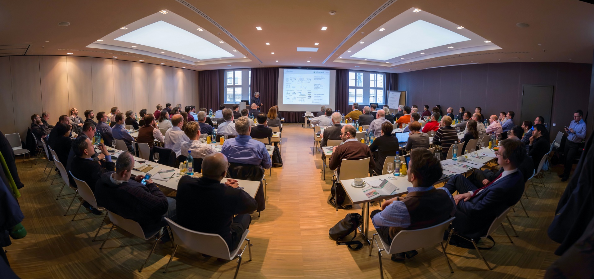
ALD in Germany: According to market estimates the equipment market alone is currently at an annual revenue of US$ 1.5 - 1.7 billion (2017) and it is expected to double in the next 4- 5 years. In a European context ALD was invented independently twice in Europe (Russia & Finland) and since the last 15 years Germany has grown to become one of the strongest European markets for ALD in R&D, chemicals, equipment and end users. Here, Dresden and Saxony isa unique ALD hotspot due to a strong semiconductor and equipment industry.
The Event will focus on the current markets for ALD, besides the leading edge semiconductor industry, applications in MEMS and Sensors, Display, Lightning, Barriers and Photovoltaics will be addressed.

Sponsors (signed so far):

CONTACT:
Dr. Katrin Ferse
Europäische Forschungsgesellschaft Dünne Schichten e. V.
Gostritzer Str. 63, 01217 Dresden, Tel. +49 351 871 8374, Fax: +49 351 8718431
E-Mail: ferse@efds.org, web: www.efds.org
Dr. Jonas Sundqvist
Fraunhofer IKTS, Dünnschicht-Technologien | Thin-Film Technologies, Winterbergstraße 28, 01277 Dresden, Germany
Telefon +49 351 2553 7693, Mobile +49 173 4394 239
E-Mail: jonas.sundqvist@ikts.fraunhofer.de
www.ikts.fraunhofer.de

CMC Conference Call for Papers - April 26-27 in Phoenix, AZ, USA
The Critical Materials Council (CMC) Conference Committee has issued a call for papers to be presented at the 2018 CMC Conference April 26-27 in Phoenix, AZ, USA. Following the annual members-only CMC meeting to be held earlier that week, the 2018 CMC Conference is open to the public.

KEYNOTE: David Bloss, Vice President, Technology and Manufacturing Group Director, Lithography Technology Sourcing, Global Supply Management, Intel Corp.
Three sessions will cover the following themes:
I. Global supply-chain issues of economics and regulations,
II. Immediate challenges of materials & manufacturing, and
III. Emerging materials in R&D and pilot fabrication.
To submit a paper for consideration, please send a 1-page abstract by January 15, 2018 to cmcinfo@techcet.com.
Attendees will include industry experts handling supply-chains, business-development, R&D, and product management, as well as academics and analysts. CMC member companies will be attending this meeting, as it is an important part of their membership.
On behalf of the CMC Conference Committee,
Lita Shon-Roy, Jonas Sundqvist, Ph.D., Ed Korczynski
Monday, October 16, 2017
ALD 2018 July 29-Wednesday, August 1 Incheon, South Korea.
The AVS 18th International Conference on Atomic Layer Deposition (ALD 2018) featuring the 5th International Atomic Layer Etching Workshop (ALE 2018) will be a three-day meeting dedicated to the science and technology of atomic layer controlled deposition of thin films and now topics related to atomic layer etching. Since 2001, the ALD conference has been held alternately in the United States, Europe and Asia, allowing fruitful exchange of ideas, know-how and practices between scientists. This year, the ALD conference will again incorporate the Atomic Layer Etching 2018 Workshop (ALE 2018), so that attendees can interact freely. The conference will take place Sunday, July 29-Wednesday, August 1, 2018, at the Songdo Convensia in Incheon, South Korea.
Link to Conference page: https://ald2018.avs.org/

TU Eindhoven present LEGO stop motion movie of a novel area-selective ALD approach
Stop motion movie of a novel area-selective ALD approach – Building a film with nanoblocks – literally! #ALDep https://t.co/pXFLgZXla9 pic.twitter.com/J9SqeNJm18— AtomicLimits (@AtomicLimits) October 12, 2017

Please find the original publication in the Atomic Limits Blog (LINK) as well as the Open Source publication below.
A. Mameli, M. J. M. Merkx, B. Karasulu, F. Roozeboom, W. M. M. Kessels, and A. J. M. Mackus, Area-selective atomic layer deposition of SiO2 using acetylacetone as a chemoselective inhibitor in an ABC-type cycle, ACS Nano 11, 9303 (2017), DOI: 10.1021/acsnano.7b04701

Saturday, October 7, 2017
ALD for coat of minitablets for effective taste masking
Atomic layer deposition—A novel method for the ultrathin coating of minitablets
International Journal of Pharmaceutics, Volume 531, Issue 1, 5 October 2017

(Picture from graphical abstract)
Abstract
We introduce atomic layer deposition (ALD) as a novel method for the ultrathin coating (nanolayering) of minitablets. The effects of ALD coating on the tablet characteristics and taste masking were investigated and compared with the established coating method. Minitablets containing bitter tasting denatonium benzoate were coated by ALD using three different TiO2 nanolayer thicknesses (number of deposition cycles). The established coating of minitablets was performed in a laboratory-scale fluidized-bed apparatus using four concentration levels of aqueous Eudragit® E coating polymer. The coated minitablets were studied with respect to the surface morphology, taste masking capacity, in vitro disintegration anddissolution, mechanical properties, and uniformity of content. The ALD thin coating resulted in minimal increase in the dimensions and weight of minitablets in comparison to original tablet cores. Surprisingly, ALD coating with TiO2 nanolayers decreased the mechanical strength, and accelerated the in vitro disintegration of minitablets. Unlike previous studies, the studied levels of TiO2 nanolayers on tablets were also inadequate for effective taste masking. In summary, ALD permits a simple and rapid method for the ultrathin coating (nanolayering) of minitablets, and provides nanoscale-range TiO2 coatings on porous minitablets. More research, however, is needed to clarify its potential in tablet taste masking applications.
Monday, October 2, 2017
The Korea Research Institute of Chemical Technology develops ALD MoS2 catalyst for hydrogen fuel
The Korea Research Institute of Chemical Technology (KRICT) has developed a core electro-catalyst design technology that can significantly improve electrochemical fuel reaction which produces hydrogen fuel.
The research team led by Dr. Kim Hyung-joo from CO2 energy vector research division at the KRICT announced on September 27 that it succeeded in developing the technology that can activate fuel reaction by changing the surface of molybdenum disulfide (MoS2) which is cheaper than white gold.
The research team led by Dr. Kim Hyung-joo from CO2 energy vector research division at the KRICT announced on September 27 that it succeeded in developing the technology that can activate fuel reaction by changing the surface of molybdenum disulfide (MoS2) which is cheaper than white gold.
Source: BusinessKorea LINK
The world´s leading foundry selects Nova VeraFlex III XF XPS for critical Logic ALD process monitoring
REHOVOT, Israel: Nova (Nasdaq: NVMI), a leading innovator and a key provider of metrology solutions for advanced process control used in semiconductor manufacturing, announced today that its most advanced XPS platform was selected by the world's leading Foundry for inline applications to be deployed in its advanced technology nodes. Revenue from this order is expected to be recognized during the third quarter of 2017.

The VeraFlex III XF combines enhanced XPS capability with a unique low
energy XRF (LE-XRF) channel to address the metrology challenges of 20nm
nodes and beyond. The VeraFlex III XF is the third generation of the
globally adopted VeraFlex series of XPS production systems. With
technology enhancements that improve performance on current inline logic
and memory film applications, the VeraFlex III XF provides solutions
for emerging applications in FinFET HKMG, interconnect processes, and
advanced memories. (http://www.novameasuring.com/veraflex3xf.html)
The VeraFlex III XF is the latest generation of the VF XPS series, which offers superior sensitivity to sub-angstrom thickness and composition characterization used for monitoring critical processes such as atomic layer deposition (ALD) at the most advanced Logic nodes.
Full story : LINK
Here's a link to the original PR:
http://ir.novameasuring.com/press_releases/novas-advanced-xps-solution-selected-by-the-worlds-leading-foundry/
Full story : LINK
Here's a link to the original PR:
http://ir.novameasuring.com/press_releases/novas-advanced-xps-solution-selected-by-the-worlds-leading-foundry/
NCD signed the large-scale contract to supply ALD equipment to Chinese DMEGC for high efficiency solar cells
NCD has just received the large-scale contract with Chinese DMEGC to supply up to 400MW solar cell manufacturing ALD equipment. This mass production equipment is several Lucida (TM) GS1600 ALD and Automation Systems to produce high efficiency crystalline solar cells with depositing fast high quality Al2O3 ALD on Si wafers. It is repeat order of the same system supplied in the production line in 2016 because the customer has been satisfied with the excellence of the system, that is, NCD’s technology and competitiveness are confirmed by the Chinese customer again. NCD is discussing supply agreements with many other customers besides this contract so is looking forward to rapid sales growth in the near future.

Lucida TM
GS1600 ALD and Automation
Subscribe to:
Posts (Atom)