Friday, December 29, 2023

ASML's New Chapter: Navigating Tech Innovation and Geopolitical Shifts Under Christophe Fouquet's Leadership

In an era of significant technological and geopolitical changes, ASML, the number one player in the semiconductor industry, stands at a crossroads. The forthcoming retirement of Martin van den Brink and Peter Wennink, who have jointly steered ASML for over a decade, signals the end of a dynamic period. Van den Brink's leadership in technology development propelled ASML to unparalleled heights in the lithography sector, while Wennink’s diplomatic and financial acumen solidified its market dominance. ASML's impact extends beyond technology; it has become a geopolitical force, enhancing the Netherlands and Europe's strategic significance in global politics.


The appointment of Christophe Fouquet as the incoming CEO heralds a new era. Fouquet faces the challenge of maintaining ASML's technological edge while adapting to a market nearing the limits of Moore's Law.
 

As ASML approaches its 40th anniversary in April 2024, it confronts a changing landscape. The company has weathered various phases – from early struggles to market leadership, marked by innovations like the PAS 5500 and immersion lithography. Under Van den Brink, ASML prioritized technological advancement, often at the expense of other factors like reliability.

The appointment of Christophe Fouquet as the incoming CEO heralds a new era. Fouquet faces the challenge of maintaining ASML's technological edge while adapting to a market nearing the limits of Moore's Law. The shift in focus from chip performance to system-level advancements requires a nuanced approach. Additionally, as technology matures, reliability and predictability become crucial for maintaining ASML's competitive edge.

The transition from a "firefighter" engineering culture to one emphasizing process and reliability won't be easy. Fouquet must balance innovation with operational efficiency, ensuring ASML remains responsive to market and geopolitical dynamics. This requires a departure from the legacy of Van den Brink, focusing instead on a holistic, structured approach to development and engineering.

Fouquet's tenure will be pivotal in shaping ASML's future. His leadership must navigate the complexities of a highly competitive industry, geopolitical pressures, and the evolving technological landscape. The challenge lies in fostering a culture that values reliability and process without stifling the innovative spirit that has been ASML's hallmark. As the company moves into its fifth decade, its ability to adapt and evolve under Fouquet's guidance will determine its continued success in a rapidly changing world.

Advancing the Microchip Revolution: EUV Lithography's Challenges and Future Outlook

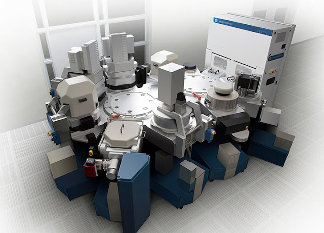
Extreme Ultraviolet (EUV) lithography represents a significant advancement in semiconductor manufacturing, enabling the production of more compact and efficient integrated circuits, particularly for 7 nm Logic process nodes and below and leading edge DRAM. This technology, developed and marketed primarily by ASML Holding, uses a highly specialized process involving laser-pulsed tin droplet plasma to etch patterns onto substrates at the 13.5 nm wavelength scale. The progression from early prototypes to more efficient models has been remarkable, with modern EUV systems capable of handling 200 wafers per hour, a substantial improvement from initial prototypes.

Looking into the future, EUV lithography is expected to play a critical role in advancing semiconductor technology, especially as the demand for smaller and more powerful chips increases. However, several technological challenges need addressing continiously to fully harness EUV's potential:

1. Optical Component Durability: The EUV process requires highly specialized and sensitive optical components, including mirrors and photomasks. These components are prone to degradation from exposure to high-energy photons and contaminants. Improving their durability and developing efficient cleaning and maintenance processes are crucial.

2. Throughput Efficiency: While significant improvements have been made, further enhancing the throughput of EUV systems is vital. This includes reducing setup times, increasing the speed of the lithography process, and minimizing downtime due to maintenance or component replacement.

3. Pattern Fidelity and Defect Reduction: As circuit patterns become increasingly smaller, maintaining pattern fidelity and reducing defects is challenging. This involves improving the resolution of EUV systems, enhancing photoresist materials to better respond to EUV exposure, and developing more effective methods to mitigate the impact of secondary electrons generated during the lithography process.

EUV Lithography - Balancing Technological Advancements with Energy Challenges

EUV lithography, pivotal in advanced semiconductor manufacturing, faces significant energy consumption challenges. The generation of EUV light, typically via laser-pulsed tin plasma, is inherently energy-intensive. Additionally, maintaining the necessary vacuum environment and cooling systems for these high-precision machines further escalates energy use. As EUV technology becomes more prevalent, especially for producing smaller, more efficient chips, optimizing energy efficiency is critical. Future developments are expected to focus on more efficient light sources, improved system design for energy conservation, and advanced thermal management, aiming to reduce the overall energy footprint of EUV lithography processes.


The semiconductor industry, traditionally known for its high environmental impact, is increasingly embracing sustainability. With the global demand for semiconductors rising, manufacturers face the challenge of scaling up production while addressing substantial water and electricity usage and managing hazardous waste from gases used in manufacturing. Historically, the focus has been on balancing power, performance, and cost. Recently, however, sustainability has emerged as a crucial consideration, with many facilities actively working to decarbonize their supply chains and reduce overall environmental impact (data from imec)

EUV Lithography's Hydrogen Demand: A Growing Concern in Chip Manufacturing

EUV Lithography, also raises concerns regarding its significant hydrogen consumption. The EUV process relies heavily on hydrogen gas to maintain the cleanliness of the optical elements, particularly for preventing tin deposition on the mirrors. The need for a continuous supply of hydrogen to facilitate this cleaning process contributes to the overall operational costs and resource demands of EUV systems. As EUV technology becomes more widespread in chip manufacturing, addressing the sustainability and efficiency of hydrogen usage will be essential, both from an environmental and economic perspective.


In EUV lithography, managing hydrogen usage presents distinct challenges. The technology requires hydrogen for removing contaminants from critical mirrors, demanding systems capable of handling high volumes while maintaining vacuum integrity. This necessity places a premium on innovative system designs that minimize the footprint and energy consumption associated with hydrogen management, directly impacting the cost and efficiency of semiconductor manufacturing. Safety considerations, given hydrogen's flammability, are paramount. Advanced, fuel-free hydrogen management strategies are employed to ensure safety and environmental compliance. These strategies focus on reducing flammability risks and eliminating the need for additional fuels, thereby minimizing carbon emissions and contributing to sustainable manufacturing practices.

Continued research and development in these areas are essential for the advancement of EUV lithography, ensuring it meets the rapidly evolving demands of the semiconductor industry.

Sources: 

Christophe Fouquet’s ASML must reinvent itself – Bits&Chips (bits-chips.nl)

www.imec.be

www.edwards.com

Wikipedia

Samsung Electronics faces challenges in securing tax breaks from the U.S. government for its new chip plant in Taylor, Texas

Samsung Electronics faces challenges in securing tax breaks from the U.S. government for its new chip plant in Taylor, Texas. Amid stiff competition from Intel, Micron Technology, and over 400 other chipmakers, Samsung's negotiations for subsidies under the $53 billion Chips and Science Act are ongoing. The plant, which will produce AI processors, has delayed its mass production start to 2025 due to rising construction costs and disappointing tax benefits. Intel, Micron, and TSMC are also investing heavily in U.S. facilities, intensifying the competition for government funding. Samsung, while not commenting on the negotiations, has highlighted its substantial U.S. investments and cooperation history at a recent event with U.S. lawmakers.

South Korea's Semiconductor Surge Signals Global Tech Revival

South Korea's semiconductor industry is experiencing a remarkable resurgence, marking a turning point in the global tech sector. In November, chip production leaped by 42%, the highest since 2017, while shipments skyrocketed by 80%, the largest increase since 2002. This upturn is a beacon of hope for giants like Samsung Electronics Co. and SK Hynix Inc. The revival extends beyond national borders, suggesting a broader recovery in global tech demand. Amidst challenges, this surge propels South Korea's industrial output and signals a brighter economic forecast for 2023, with emerging technologies fueling further growth.


Source: South Korea Chip Output Jumps in Sign of Returning Global Demand - Bloomberg

TSMC Set to Revolutionize Chip Technology with Trillion-Transistor Packages by 2030

In a groundbreaking announcement at IEDM, TSMC has unveiled ambitious plans to develop chip packages harboring over one trillion transistors and monolithic chips with more than 200 billion transistors by 2030. This visionary goal is set to be achieved through the development of advanced production nodes, including 2nm-class N2 and N2P, and even finer 1.4nm-class A14 and 1nm-class A10 processes. Despite the slowdown in process technology development and existing technical and financial challenges, TSMC remains optimistic about accomplishing these targets within the next five to six years. The company, renowned as the world's largest semiconductor foundry, is confident in overcoming industry hurdles to bring these complex, multi-chiplet systems and more intricate monolithic chips to the forefront of technology. This development signals a significant leap in chip architecture, promising transformative advancements in the tech industry.


Source:

Rising Tide in AR/VR Market: New Era of Spatial Computing Begins Amidst Challenges

The augmented reality (AR) and virtual reality (VR) market is witnessing a resurgence of interest, particularly with the industry's pivot towards the metaverse. Key players like Meta and Apple are at the forefront, with Apple's launch of Vision Pro marking a new phase in spatial computing. This technology is widely viewed as the next evolutionary step in 3D digital interaction.


Source: DSCC

Despite the enthusiasm, the market reality has lagged behind expectations. According to a recent IDC report, global AR/VR headset shipments have seen a consistent decline, dropping 44.6% year-over-year in the second quarter of 2023. This trend highlights the challenges in boosting demand and adoption rates. A critical area for growth lies in innovative display technologies, crucial for developing AR/VR products.


The Quest 3's design is an evolution of that of the Quest 2, combined with elements of the Meta Quest Pro. It uses a pair of LCD displays with a per-eye resolution of 2064×2208 (an increase over the 1832×1920 resolution of the Quest 2), viewed through pancake lenses similar to the Quest Pro to enable a thinner enclosure. The face of the headset is adorned with three "pills" containing sensors and cameras; the two outer pills each contain a monochrome camera used for positional tracking, and a color camera used for mixed reality passthrough. The center pill contains a depth sensor, which is used in combination with other sensors to sense the user's surroundings for boundaries and mixed reality experiences. The Quest 3 uses the Snapdragon XR2 Gen 2, a system-on-chip manufactured by Qualcomm and based on their Snapdragon 8 Gen 2 flagship mobile phone SoC. which Meta has touted as having more than twice the raw graphics (GPU) performance of the Snapdragon XR2 Gen 1 used by the Quest 2 and other similar standalone headsets

The future, however, looks promising. Guillaume Chansin of DSCC anticipates a significant uptick in the AR/VR headset market over the next five years, beginning in 2024. This optimism is fueled by expectations of advanced headsets powered by Qualcomm's Snapdragon XR2 Gen 2, alongside new offerings from Meta, ByteDance, and Apple. Despite a steep price tag, Apple's Vision Pro, equipped with optical inserts from Zeiss, is expected to make a mark in the market.


Apple Vision Pro is an upcoming mixed-reality headset developed by Apple Inc. It was announced on June 5, 2023, at Apple's Worldwide Developers Conference, with availability scheduled for early 2024 in the United States and later that year internationally. It is Apple's first product in another major category since the Apple Watch in 2015

The shift towards multiple displays in AR/VR products is another notable trend, with most devices incorporating dual displays. DSCC projects a staggering increase in display shipments for AR/VR, reaching 124 million units by 2028. While VR is set to dominate consumer spaces, see-through AR will be more prevalent in professional settings.

The battle of display technologies is central to this evolution. While VR and pass-through AR mostly rely on TFT LCD and AMOLED, MicroOLED has started to make inroads. MicroOLED, particularly favored by Apple's Vision Pro, offers high resolution and luminance, crucial for an enhanced user experience. Additionally, the emerging MicroLED technology, known for its high brightness and reliability, is poised to revolutionize see-through AR displays.

Despite these advancements, the AR/VR market continues to grapple with challenges in display technology. Innovations in Micro OLED and MicroLED are essential to overcome these hurdles and drive market growth. As the industry continues to evolve, these technologies will play a pivotal role in shaping the future of spatial computing.

ALD offers significant advantages in Micro OLED and MicroLED display manufacturing. Its ability to deposit ultra-thin, uniform layers is crucial for layer uniformity and display quality. ALD is pivotal for creating barrier layers in Micro OLEDs, protecting them from environmental degradation, and for depositing dielectric layers in MicroLEDs, essential for improving efficiency and reducing pixel cross-talk. Additionally, ALD enhances light extraction, encapsulation, and interface engineering, crucial for flexible and transparent displays. While initially costly, ALD's scalability and material diversity make it a key technology for advancing Micro OLED and MicroLED displays, potentially reducing overall manufacturing costs and enhancing display longevity and performance.

Sources: 

MicroOLED and MicroLED: The Future of AR/VR Displays – Display Daily

Wikipedia

Wednesday, December 27, 2023

Exploring Ultrathin Solar Cells with Professor Carl Hägglund: A Journey from Stanford's ALD Techniques to Plasmonic Solar Cell Optimization

In this episode, Tyler is joined by Professor Carl Hägglund from Uppsala University. They discuss Carl’s motivations for pursuing ultrathin solar cells, how he learned ALD at Stanford in Stacey Bent’s lab, and an unlikely research connection through his child’s school. They also talk about why ALD is useful for plasmonic solar cells, optimization of SnS ALD and his planned path towards a fully realized ultrathin photovoltaic.


00:00 Introduction
01:45 Motivation for fabricating plasmonic solar cells
09:58 Learning ALD at Stanford
22:46 Optimizing SnS ALD process
30:33 Path towards an ultrathin solar cell

Wednesday, December 20, 2023

Enhancing Thin Film Deposition with Plasma-Activated Water: A Novel Approach in Atomic Layer Deposition

The research article "Novel Energetic Co-Reactant for Thermal Oxide Atomic Layer Deposition: The Impact of Plasma-Activated Water on Al2O3 Film Growth" presents a groundbreaking study on the use of plasma-activated water (PAW) in the atomic layer deposition (ALD) of Al2O3 thin films. This study offers significant insights into the potential advantages of using PAW over traditional water in thin film deposition processes.


One of the key findings of this research is the enhanced Growth Per Cycle (GPC) when using PAW as a co-reactant. The study found that PAW led to an increase in GPC of up to 16.4% compared to deionized (DI) water. This enhancement is attributed to the reactive oxygen species present in PAW, such as H2O2 and O3, which are believed to activate substrate sites more effectively, thereby improving both the GPC and the overall quality of the films.

The study also delves into the chemical reactivity of PAW, noting significant changes in its physicochemical properties upon activation. These changes include a decrease in pH, indicating increased acidity, as well as increases in oxidation-reduction potential (ORP), conductivity, and total dissolved solids (TDS). Additionally, the concentration of reactive species like H2O2, NO2−, NO3−, HNO2, and O3 was found to be higher in PAW.

The improved film quality achieved with PAW is another highlight of the study. Films grown using PAW, especially with PAW at a pH of 3.1, displayed a near-stoichiometric O/Al ratio, reduced carbon content, and an expanded bandgap. These characteristics are indicative of a superior film quality compared to those grown using DI water.

Furthermore, the study suggests that a comprehensive understanding of PAW's role in ALD necessitates further investigations. These investigations should explore different temperatures, metal precursors, and PAWs generated by alternate non-thermal plasmas.

The term “PAW-ALD” has been proposed to describe this enhanced variant of the ALD process that incorporates plasma-activated water. This new descriptor highlights the unique approach and potential benefits of using PAW in thin film deposition processes.

Finally, the potential applications of this research are significant. The use of PAW in ALD could mirror the gains observed in plasma-enhanced atomic layer deposition (PEALD) processes that use oxygen plasma, indicating its potential industrial relevance.

Source: 

Nanomaterials 202313(24), 3110; https://doi.org/10.3390/nano13243110

Nanomaterials | Free Full-Text | Novel Energetic Co-Reactant for Thermal Oxide Atomic Layer Deposition: The Impact of Plasma-Activated Water on Al2O3 Film Growth (mdpi.com)

Announcement: Webinar on ALD and MLD Techniques for Advanced Functional Materials

Join us for an enlightening webinar on Atomic Layer Deposition (ALD) and Molecular Layer Deposition (MLD), showcasing their combined prowess in the creation of novel inorganic-organic materials. This event is an excellent opportunity for those interested in advanced material sciences and engineering.


Date and Time: Tuesday, 16th of January, 2024 at 14:00 CET

Duration: 45 minutes

This session will provide a comprehensive overview of ALD and MLD, contrasting them with traditional solution-based methods. We will delve into how these techniques enable the formation of high-quality thin films, crucial for practical applications in areas such as optical data storage and wearable energy harvesting devices.

Key Highlights:

- An introduction to ALD-MLD techniques.

- Exploration of state-of-the-art inorganic-organic thin films, including photoactive ferrimagnetic and thermoelectric hybrid thin films.

- Discussion on technical challenges with organic precursors and solutions for industrial-scale application.


Guest Speaker: Topias Jussila, Doctoral Researcher, Aalto University

Topias Jussila is a promising PhD student at the Department of Chemistry and Materials Science, Aalto University, Finland. With a background in Chemistry and Functional Materials, his current research focuses on the development of novel thin film materials using ALD and MLD, particularly in the realm of iron-based materials.


Don't miss this opportunity to gain insights into the cutting-edge world of thin film materials and their applications. Register today to secure your spot!


For more information and registration, visit Atomic layer deposition (ALD) and molecular layer deposition (MLD) together present an elegant technique for the deposition of novel inorganic-organic materials. (picosun.com)

Friday, December 15, 2023

Tokyo Electron Develops an Extreme Laser Lift Off Technology That Contributes to Innovations in 3D Integration of Advanced Semiconductor Devices

Tokyo Electron (TEL; Head Office: Minato-ku, Tokyo; President: Toshiki Kawai) announced that a development team at Tokyo Electron Kyushu, - the development and manufacturing site for wafer bonder/debonder systems- has developed an Extreme Laser Lift Off (XLO) technology that contributes to innovations in 3D integration of advanced semiconductor devices adopting permanent wafer bonding. This is a new technology for two permanently bonded silicon wafers that uses a laser to separate the top silicon substrate from the bottom substrate with integrated circuit layer.

The progress of digital society is raising expectations for greater improvement in semiconductor chip performance. As a result, the next-generation semiconductors being introduced feature further scaling and higher integration as well as advancements in 3D integration using the permanent wafer-to-wafer bonding technology. In the current permanent wafer bonding sequence, two wafers with integrated circuits on their surface are permanently bonded together before going through a grinding process, in which the top wafer is thinned and removed. Since advanced semiconductor devices require an increasing number of stack layers, there is a growing concern that the grinding process may decrease the yield due to factors such as the stress on wafers while grinding, delaminating of films after grinding and widening of the edge trimming area (which reduces the number of viable chips on a wafer). For these reasons, technological innovation is required with a different approach from grinding technology.

TEL’s breakthrough Extreme Laser Lift Off technology replaces the current wafer thinning and removal process that relies on grinding, thereby enabling removal of the top silicon wafer without the yield concerns associated with the existing process.


The Extreme Laser Lift Off technology simplifies the wafer thinning process by replacing and eliminating multiple existing steps, including backside grinding, polishing and chemical etching of silicon wafer. Compared with the grinding process, the Extreme Laser Lift Off process does not require deionized water, which leads to an over 90% reduction in water consumption and a significant drop in the drain water, contributing to mitigate the environmental load. Furthermore, we are developing a technology to properly treat and reuse the top silicon substrate separated by Extreme Laser Lift Off, which can help reduce the CO2 emissions from wafer fabrication.

Continually adhering to pursue the motto of Best Products, Best Technical Service, TEL will keep contributing to technological innovation in semiconductors. As we celebrated the 60th anniversary of our founding this year, we take this milestone as a new starting point for our further challenge and evolution to contribute to the development of a dream-inspiring society.

Wednesday, December 13, 2023

Breakthrough in Digital Lithography by Applied Materials and Ushio Boosts AI Computing Power

Ushio, Inc. have announced a significant strategic partnership, marking a new era in digital lithography technology. This collaboration aims to spearhead the transition to heterogeneous chiplet integration on large substrates like glass, a move crucial for advancing Artificial Intelligence (AI) computing capabilities.


This new digital lithography system, pioneered by Applied Materials and Ushio, is tailor-made for patterning advanced substrates vital in the AI era. With the growing demand for AI workloads, there's an increased need for larger, more functional chips. Traditional methods can't keep up with AI's performance requirements, hence the shift to heterogeneous integration (HI) techniques. These involve combining multiple chiplets in an advanced package, offering performance and bandwidth comparable to monolithic chips.


The partnership leverages Applied Materials' expertise in large substrate processing and Ushio's experience in lithography for packaging. Dr. Sundar Ramamurthy from Applied Materials highlights the new Digital Lithography Technology (DLT) as a game-changer for customers' advanced substrate roadmaps. William F. Mackenzie of Ushio emphasizes their long-standing experience in lithography systems and their commitment to this new venture.

The DLT system stands out as the only technology capable of achieving the necessary resolution for advanced substrate applications while maintaining high-volume production throughput. It can pattern line widths less than 2-microns, allowing unprecedented area density for chiplet architectures on various substrates, including glass.

Applied Materials is responsible for R&D and creating a scalable roadmap for the DLT system, aiming to push innovation in advanced packaging to 1-micron line widths and beyond. Ushio will use its established manufacturing and customer infrastructure to facilitate the technology's adoption.

While this announcement is forward-looking and subject to the usual risks and uncertainties of the tech industry, it heralds a new chapter in computing technology, potentially transforming the landscape of high-performance computing in the AI era.

- Applied Materials, Inc. is a leader in materials engineering solutions, essential in producing new chips and advanced displays worldwide.

- Ushio, Inc., established in 1964, specializes in manufacturing and selling various light sources and optical equipment, with a significant presence in industrial processes and visual imaging.

For more information or media inquiries, contact Ricky Gradwohl for Applied Materials and the Corporate Communication Department for Ushio. 

Photos and more details are available on here Breakthrough Digital Lithography Technology From Applied Materials and Ushio to Enable More Powerful Computing Systems for the AI Era | Applied Materials.

Monday, December 11, 2023

Intel Showcases Groundbreaking Transistor Innovations at IEDM 2023

At the 2023 IEEE International Electron Devices Meeting (IEDM), Intel introduced significant advancements in transistor technology that continue to drive Moore's Law forward. Intel's Components Research group demonstrated innovative 3D stacked CMOS transistors, enhanced with backside power and direct backside contacts. This breakthrough in transistor architecture allows for more efficient scaling and improved performance, marking a first in the industry.

3D Stacked CMOS Transistors

Intel displayed the ability to vertically stack complementary field effect transistors (CFET) with a scaled gate pitch down to 60 nanometers (nm). This technology, combined with backside power and direct backside contacts, underscores Intel's leadership in gate-all-around transistors and its capacity to innovate beyond RibbonFET.


Beyond Five Nodes in Four Years

Intel's PowerVia, set for manufacturing readiness in 2024, represents the first implementation of backside power delivery. At IEDM 2023, the company identified ways to extend and scale backside power delivery beyond PowerVia, utilizing backside contacts and other novel vertical interconnects for efficient device stacking.

Integration of Silicon and GaN Transistors

Intel successfully integrated silicon transistors with gallium nitride (GaN) transistors on the same 300 mm wafer. The "DrGaN" technology showcased at the event demonstrates Intel's advancements in high-performance integrated circuits for power delivery.

Advances in 2D Transistor Space

Intel presented high-mobility transition metal dichalcogenide (TMD) 2D channel materials, showcasing prototypes of high-mobility TMD transistors for both NMOS and PMOS. Additionally, Intel revealed the world’s first gate-all-around (GAA) 2D TMD PMOS transistor and the first 2D PMOS transistor fabricated on a 300 mm wafer.


These developments by Intel represent a significant stride in semiconductor research, promising to enhance the efficiency and capabilities of future computing technologies.

Friday, December 8, 2023

IBM and Samsung Revolutionize Semiconductor Industry with Groundbreaking VTFET Transistor Technology

In a breakthrough development, IBM and Samsung have introduced a new transistor architecture named Vertical-Transport Nanosheet Field-Effect Transistors (VTFETs), potentially outperforming traditional FinFETs. This exciting innovation was discussed in the AAC Exclusive article, "A Chat With IBM Researchers Who Built the New 'VTFET' Transistor," featuring insights from IBM researchers Brent Anderson and Hemanth Jagannathan.


Comparison of a VTFET (left) vs. a lateral FET (right) transistor with current flowing through them. FinFETs have a limited gate pitch, scaled down to ~48nm, while VTFETs offer more scaling potential with a longer gate length due to their vertical design.

VTFETs offer significant improvements in performance and area scaling, potentially reducing energy usage in devices by up to 85% compared to FinFETs. These transistors operate with a vertical orientation, allowing for longer gates and thicker spacers and source-drains, which reduce resistance and capacitance. This design enables smaller transistor size while enhancing performance.

Anderson and Jagannathan's roles at IBM have been pivotal in the development of VTFETs. Anderson, who joined IBM in 1991, has been instrumental in driving the technology design for various logic nodes, including VTFET. Jagannathan, with IBM for 15 years, has managed process technology groups and played a crucial role in hardware research for VTFET.

Their work signifies a significant step forward in semiconductor technology, promising higher density, performance, and energy efficiency. This innovation represents a potential future for Moore's law scaling, alongside other advancements like monolithic 3D and chip stacking technologies. The real-world implementation of VTFETs is eagerly anticipated, with the technology expected to mature in the coming years.


Thursday, December 7, 2023

Applied Materials and CEA-Leti Forge New Joint Lab to Spearhead Specialty Chip Market Innovations

Applied Materials and CEA-Leti have announced a significant expansion of their collaboration, focusing on innovative materials engineering solutions tailored for specialty semiconductor markets. The joint lab, situated at CEA-Leti, is dedicated to propelling semiconductor device development, particularly for Applied Materials' ICAPS (IoT, Communications, Automotive, Power, and Sensors) customers.

This partnership underscores a growing demand in the ICAPS sector, fueled by advancements in industrial automation, IoT, electric vehicles, and green energy initiatives. The joint lab will tackle various materials engineering challenges to facilitate the next generation of ICAPS device innovations. Equipped with Applied Materials' advanced 200mm and 300mm wafer processing systems, the lab leverages CEA-Leti's expertise in new materials evaluation and device validation.


The joint lab features several of Applied Materials’ 200mm and 300mm wafer processing systems, such as this Endura® system, and leverages CEA-Leti’s world-class capabilities for evaluating performance of new materials and device validation.​

The collaboration aims to enhance power efficiency, performance, and cost-effectiveness, while also reducing time to market. Aninda Moitra, corporate vice president and general manager of Applied Materials' ICAPS business, emphasizes this initiative as an extension of a decade-long successful partnership, geared towards accelerating innovation in specialty semiconductor technologies.

Sébastian Dauvé, CEO of CEA-Leti, reflects on the decade of collaborative projects leading up to this new joint lab. These projects spanned advanced metrology, memory materials, optical devices, bonding techniques, and chemical-mechanical planarization. The results have consistently delivered high value, setting a solid foundation for this expanded engagement.

The lab not only aims to develop unique technological solutions for Applied Materials' customers but also supports CEA-Leti's internal R&D programs, overcoming current technical challenges. This initiative marks a significant step in the collaboration, promising to bring breakthroughs in specialty semiconductor technology to global markets.

Wednesday, December 6, 2023

ASM International Announces $300M Expansion in Arizona, Boosted by Dutch-U.S. Collaboration with Prime Minister Mark Rutte's Support

ASM International N.V. is set to expand its U.S. operations with a €300 million investment in a new facility in Scottsdale, Arizona. This expansion, covering more than 20 acres, aims to bolster their research, technology development, and manufacturing capabilities in the semiconductor industry. The state-of-the-art site, spanning 250,000 square feet, will host various functions, emphasizing renewable energy and sustainability.


A rendering of the new ASM HQ (source ASM America)

This move marks a significant step in reinforcing Arizona's position as a hub for semiconductor innovation and highlights the strong Arizona-Netherlands partnership. Notably, Mark Rutte, Prime Minister of the Netherlands, emphasized the importance of this expansion in strengthening cross-border collaborations and the global semiconductor value chain. The initiative is viewed as pivotal in fostering Dutch-U.S. partnerships and propelling advancements in the industry.

“Arizona and the U.S. are valuable partners in the Netherlands’ mission to co-create solutions that promote innovation and partnerships in the global semiconductor value chain,” said Mark Rutte, Prime Minister of the Netherlands. “It is through these types of cross-border collaborations that we are shaping the future of advancements in this growing industry.”

The new facility will create approximately 500 new jobs over six years, focusing on engineering and research roles. ASM's commitment to sustainability is evident in its plans for LEED certification and water reuse programs. Additionally, the company has formed partnerships with local organizations for environmental conservation efforts, showcasing its dedication to community and environmental stewardship. This expansion by ASM International is set to significantly enhance semiconductor technology and innovation, highlighting the growing synergy between the U.S. and the Netherlands in this vital sector.
Source:

Saturday, December 2, 2023

Introducing ALD to the Semiconductor Industry with Suvi Haukka – ALD Stories Ep. 29

Dr. Suvi Haukka, former executive technologist at ASM, ASM Fellow and ALD Innovator Awardee, joins Tyler for Episode 29. Suvi began her ALD career at Microchemistry in Finland working on atomic layer epitaxy on catalysts for under the direction of ALD technology inventor, Tuomo Suntola. She continued with Microchemistry as head of the thin film development group before spending most of her time teaching the world’s biggest semiconductor companies, like Intel and Samsung, about ALD. Suvi is one of the integral people in introducing ALD to the semiconductor industry in the 2000s. Suvi and Tyler discuss how she started working with ALD, what it was like to do a PhD with Tuomo Suntola, and how the make up of Microchemistry changed over the years. We also discuss the circumstances surrounding the ASM acquisition, how development changed under new leadership, and how it felt pitching ALD to the semiconductor industry. 


In this episode: 
00:32 Introduction to Microchemistry 
06:01 Doing a PhD with Tuomo Suntola 
19:00 Visiting semiconductor companies 
25:37 Post-ASM acquisition

Friday, December 1, 2023

ASD2024: Uniting the World of Area Selective Deposition in Historic Old Montreal

Announcement for ASD2024 Workshop

Dates: April 15-16, 2024

Location: Old Montreal, Canada

Welcome and bienvenue to the exciting Area Selective Deposition (ASD) workshop to be held in the picturesque Old Montreal. This two-day event, scheduled for April 15 and 16, offers an enriching platform for both academic and industry professionals to exchange groundbreaking ideas in the field of ASD.


Special Sessions:

1. Pre-Workshop Tutorial: A comprehensive half-day tutorial on April 14 (Sunday afternoon). Note: This session requires an additional fee.

2. Atomic Layer Processing Showcase: A half-day event on April 17 (Wednesday morning), highlighting Canada's advancements in atomic layer processing. This session is included in the conference fee.


Conference Venues:

- Hotel Place d'Armes (55 Rue Saint-Jacques): Main sessions and lunches on Monday and Tuesday will be hosted here. This 4-star hotel is conveniently located near a metro stop.

- Hotel Nelligan (106 Saint-Paul St W): A 4-star boutique hotel, the venue for the opening mixer on Sunday evening and the poster session on Monday evening.

Workshop Highlights:

- Single session format over two days featuring invited and contributed talks.

- A panel discussion focusing on the industrial and academic communication of ASD.

- Networking opportunities with leading experts and peers.

Explore Montreal:

Participants are encouraged to experience the charm of Old Montreal, known for its vibrant restaurants, bars, shopping venues, and historical sites like the Notre Dame Basilica and the port. For sports enthusiasts, the Circuit Gilles Villeneuve offers a unique opportunity for running and cycling.

Organizers:

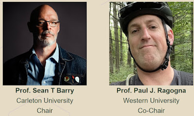
- Prof. Sean Barry, Carleton University

- Prof. Paul Ragogna, Western University


Scientific Committee:

- Adrie Mackus, Eindhoven University of Technology

- Anjana Devi, Ruhr University Bochum

- Annelies Delabie, IMEC

- Anuja DaSilva, Lam Research

- Dennis Hausmann, Lam Research

- Erwin Kessels, Eindhoven University of Technology

- Gregory Parsons, North Carolina State University

- Han-Bo-Ram Lee, Incheon National University

- Ishwar Singh, IBM

- Keyvan Kashefi, Applied Materials

- Kristen Colwell, Intel

- Mark Saly, Applied Materials

- Marko Tuominen, ASM

- Ralf Tonner-Zech, Wilhelm-Ostwald-Institute für Physikalische und Theoretische Chemie

- Ravi Kanjolia, EMD Electronics

- Robert Clark, TEL

- Sang Hoon Ahn, Samsung Electronics

- Seung Wook Ryu, SK hynix

- Stacey F. Bent, Stanford University

Contact Information:

asd2024.ca

Wednesday, November 29, 2023

Launch of the Oxford Instruments Innovation Centre: Advancing Scientific Research and Collaboration

The Oxford Instruments Innovation Centre, a state-of-the-art facility, has been launched at its High Wycombe site. This Centre consolidates Oxford Instruments' analytical innovations, aligning with its mission of fostering a greener, healthier, more connected society. The inauguration welcomed dignitaries like Countess Howe, Lord-Lieutenant of Buckinghamshire, and Cllr. Paul Turner, Mayor of High Wycombe, alongside prominent figures from academia and industry. Dr. Ian Wilcock, Managing Director, led the opening, showcasing the Centre's role in advancing scientific research in various fields. The facility, a collaboration hub, allows access to cutting-edge technology and expertise. Oxford Instruments, a pioneer since 1959 and a significant contributor to Nobel-prize winning research, continues to impact science, particularly in material analysis, underlining its global technological leadership.


Source: Oxford Instruments Launches Innovation Centre - Oxford Instruments (oxinst.com)

Monday, November 27, 2023

Congratulations to Jusung Engineering on 30 Years of Pioneering Innovation and Market Leadership in ALD, Semiconductor, Display, and Solar Technologies!

Jusung Engineering, celebrating its 30th anniversary, is a leader in semiconductors, displays, and solar equipment. Founded in 1993, the company has seen considerable growth through innovation, achieving record sales and operating profits last year. It specializes in semiconductor equipment for memory and non-memory sectors, leveraging advanced ALD technology. In displays, Jusung is diversifying equipment for various panel sizes, while in solar, it's innovating with high-efficiency solar cells. The company is investing in future growth, with new R&D and manufacturing facilities, focusing on technological independence. It holds over 3,000 patents, with 65% of its workforce in R&D, investing 15-20% of sales in technology development. The CEO attributes their success to relentless innovation and a unique path, with plans to maintain leadership in future technologies and expand into global markets. Despite recent challenges, Jusung remains optimistic, prioritizing innovation and market creation.


The Jusung Engineering headquarters in Gwangju, Korea 출처 : Businesskorea (https://www.businesskorea.co.kr)

Fullarticle and interview:

Jusung Engineering Leading in Semiconductor, Display, Solar by Innovating with Atomic Layer Deposition - Businesskorea

Friday, November 24, 2023

AIXTRON Launches €100 Million Innovation Center to Boost Semiconductor Technology Development

AIXTRON SE, a leader in deposition equipment for the semiconductor industry, has begun constructing a new EUR 100 million innovation center at its headquarters in Herzogenrath, Germany. This significant investment will establish a 1000m2 cleanroom, along with space for metrology equipment, incorporating cutting-edge industry technologies. Scheduled for initial use in the second half of 2024 and official handover in early 2025, this facility marks a major milestone in AIXTRON's 40-year history. The innovation center, celebrated during a ground-breaking ceremony attended by political, scientific, and industry representatives, reinforces AIXTRON’s commitment to leading semiconductor technology and future growth. 

Dr. Felix Grawert, CEO of AIXTRON, highlighted the center's role in developing next-generation solutions for digitalization, electromobility, and energy efficiency. The cleanroom, classified as ISO 6 with potential expansion to ISO 4, is designed for high efficiency, utilizing a compact, multi-level layout to maximize space and streamline processes.


About AIXTRON

AIXTRON SE is a leading provider of deposition equipment to the semiconductor industry. The Company was founded in 1983 and is headquartered in Herzogenrath (near Aachen), Germany, with subsidiaries and sales offices in Asia, United States and in Europe. AIXTRON´s technology solutions are used by a diverse range of customers worldwide to build advanced components for electronic and optoelectronic applications based on compound or organic semiconductor materials. Such components are used in a broad range of innovative applications, technologies and industries. These include Laser and LED applications, display technologies, data transmission, SiC and GaN power management and conversion, communication, signaling and lighting as well as a range of other leading-edge applications.

Our registered trademarks: AIXACT®, AIXTRON®, Atomic Level SolutionS®, Close Coupled Showerhead®, CRIUS®, Gas Foil Rotation®, OVPD®, Planetary Reactor®, PVPD®, TriJet®

For further information on AIXTRON (FSE: AIXA, ISIN DE000A0WMPJ6) please visit our website at www.aixtron.com

Oxford Instruments Secures Major Orders for GaN ALE & ALD Systems from Leading Japanese Power Electronics and RF fabs

Oxford Instruments has received significant orders for its GaN ALE (Atomic Layer Etch) and ALD (Atomic Layer Deposition) systems from major Japanese foundries specializing in power electronics and RF (Radio Frequency). These systems are essential for producing GaN (Gallium Nitride) HEMT (High Electron Mobility Transistor) devices, catering to rapidly growing markets such as consumer fast-charging, data centers, and 5G/6G communications.


Oxford Instruments Plasma Technology staff at ALD2018/ALE2018 in Korea (Looking Back on ALD/ALE 2018 - Oxford Instruments (oxinst.com))

The company's ALD technology is known for its high throughput and low damage plasma processing, enhancing film and interface quality. It is widely used by leading GaN HEMT device manufacturers globally. The ALE solution, particularly for p-GaN HEMTs, is production-qualified and offers precise etching with minimal damage, featuring Etchpoint®, a unique endpoint detection technology developed in collaboration with LayTec AG.


Atomic Scale Processing

Etchpoint® allows for automated transition from standard high-rate etching to low damage ALE, improving device reliability. It enables precise AlGaN recess etches, crucial for the next generation GaN MISHEMT E-mode devices, with an accuracy of ±0.5 nm. These technologies can be integrated into an automated handler for multi-chamber processing without breaking vacuum, enhancing device performance and yield at a lower cost.


Gallium Nitride (GaN) provides higher breakdown strength, faster switching speed, and higher thermal conductivity for power electronics and RF applications. To support the high-volume manufacture of reliable GaN HEMT devices, Oxford Instruments in collaboration with LayTec have developed and optimised a new etch-depth monitoring solution to reliably fabricate GaN HEMT device structures. PlasmaPro 100 ALE with Etchpoint® system provides low damage etching with surface smoothing with unparalleled accuracy in target etch depth for devices such as p-GaN HEMTs and recessed gate MISHEMTs. Etchpoint is fully integrated with both the hardware and software of the PlasmaPro 100 ALE system, offering unrivalled accuracy of etch layer depth for GaN and AlGaN.

Dr. Aileen O'Mahony, GaN Product Manager at Oxford Instruments Plasma Technology, highlighted the significance of these orders from Japan, emphasizing the optimization of their ALD solution for GaN-surface plasma pre-treatment and the implementation of ALE with Etchpoint®. These developments are crucial in addressing complex challenges in device manufacturing while ensuring high throughput, reliability, and uptime in production.


Thursday, November 23, 2023

AI-Driven Chip Demand Spurs Optimism in Semiconductor Industry; Analyst Upgrades Key Players with Bullish Price Targets

Analyst Timm Schulze-Melander (Head of Tech Hardware research, Redburn) predicts growth in the semiconductor equipment industry, driven by AI-related chip demand. He upgraded Applied Materials and ASM International to "Buy," started Lam Research with a "Buy" rating, and rated KLA as "Neutral." Despite current capacity reductions, he sees growth resuming in 2025. Positive signs include recovering PC and mobile phone markets, with smartphone shipments expected to rise. He set price targets for each company, highlighting their market strengths. This analysis led to a rise in the companies' stock prices, reflecting optimism for the sector's future, particularly in the context of AI-driven demand.

The target prices set by analyst Timm Schulze-Melander are as follows:
  • Lam Research: $800 - now $717
  • ASM International: €545 - now $459
  • KLA: $550 - now $554
  • Applied Materials: $175 - now $149


Sources: 
Google Finance

Wednesday, November 22, 2023

SEMICON Europa 2023: A Deep Dive into ALD Technology for Wafer Fab Equipment in the More-than-Moore Era

Last week at SEMICON Europa, at the ALD Tech Day Organized by Beneq, Yole Group presented a comprehensive analysis on ALD technology for More-than-Moore (MtM) devices, focusing on its impact and future in the wafer fab equipment market. The presentation titled "Atomic Layer Deposition for More-than-Moore Devices in a Perspective of the Wafer Fab Equipment Market" offered valuable insights into the current trends and future directions of this pivotal technology.

The Growing Importance of ≤200 mm Wafers

A focal point of the discussion was the ≤200 mm wafer size, a segment that remains crucial in the semiconductor industry despite the surge in larger wafer sizes. The presentation highlighted the market size, chipmaker revenue, and capacity expansion specifically for this category. It emphasized that while the industry continues to evolve technologically, the demand for ≤200 mm wafers remains robust, accounting for a significant portion of the market.

Semiconductor Device Revenue Projections

Yole Group presented a detailed forecast for semiconductor device revenue, segmenting it by device type. They projected a CAGR of approximately 4.5%, expecting the overall market to reach around $850 billion by 2030. Within this, MtM devices are anticipated to contribute significantly, estimated at about $270 billion, indicating the growing relevance of these devices in the semiconductor landscape.


CapEx 200 mm Accelerates in Coming 5-Years - In 2023, the CapEx for 200mm wafer processing stood at $37 billion, representing 15% of the total device revenue of $252 billion. The slide forecasts an increase in CapEx to 17% of revenue by 2025, followed by an expected decrease to more sustainable levels by 2028. An impending demand for more Wafer Fab Equipment (WFE) for 200mm processing. Importantly, a significant opportunity for the introduction of ALD technologies in fabrication facilities, driven by the growth of compound semiconductors. This suggests a strategic shift in the industry, emphasizing the expanding role of ALD technology.

Capital Expenditure Trends and ALD Market Dynamics

The presentation also shed light on the capital expenditure (CapEx) trends in the industry, particularly for 200 mm wafer processing. With CapEx projected to increase to 17% of the revenue by 2025, a subsequent trend towards more sustainable levels by 2028 was also anticipated. This trend underscores the expanding market and the need for more Wafer Fab Equipment (WFE), presenting a substantial opportunity for the growth of ALD technologies.

Atomic Layer Deposition: Meeting Industry Needs

The analysis delved deeply into the ALD market, discussing how this technology is evolving to meet the changing demands of the semiconductor industry. It was pointed out that ALD technology is not just adapting but also driving significant advancements, particularly in the context of MtM devices.


From the presentation by Yole Group focuses on the use of ALD in power devices, emphasizing its role in enhancing device performance through precise interface control. The need for specialized ALD equipment, capable of handling multiple processes and materials, including thermal and plasma ALD with various precursors. ALD applications are found in in Silicon Carbide (SiC) and Gallium Nitride (GaN) devices, covering aspects like passivation, substrate creation, and buffer layers. While ALD is still in R&D for GaN High Electron Mobility Transistors (HEMT), it is already being used for SiC Trench and Planar MOSFETs in encapsulation and gate dielectrics, signaling its growing importance in semiconductor manufacturing.

Industry Challenges and Opportunities

The challenges and opportunities within the semiconductor industry were a crucial part of the discussion. The presentation addressed the current supply chain dynamics, technological innovations, and market trends that are shaping the adoption and development of ALD technology.

Conclusion

The presentation at SEMICON Europa provided a lucid and detailed perspective on the ALD technology in the context of the wafer fab equipment market. With a focus on ≤200 mm wafer size, it painted a comprehensive picture of the current market scenarios, future trends, and the pivotal role of ALD technology in shaping the future of semiconductor manufacturing. As the industry continues to evolve, the insights from this presentation will undoubtedly influence strategic decisions and technological advancements in the semiconductor sector.

SourceALD TECHDAY 2023 powered by Beneq (yolegroup.com)

Presentation shared with the attendees

AIXTRON's G10-GaN System Empowers BelGaN's Expansion into the Growing GaN Semiconductor Market

The article discusses AIXTRON's support for BelGaN in expanding its Gallium Nitride (GaN) business through the new G10-GaN system. AIXTRON SE, a semiconductor company, is enabling BelGaN, a leading GaN automotive-qualified semiconductor foundry in Europe, to enter the growing GaN market and boost GaN technology innovation. BelGaN plans to use AIXTRON's G10-GaN, which offers top performance, a compact design, and low cost per wafer, starting with an 8x150mm configuration, to be delivered to BelGaN's production site in Oudenaarde, Belgium, by the end of 2023. This system will later evolve to support 5x200mm.


AIXTRON's G10-GaN System Empowers BelGaN's Expansion into the Growing GaN Semiconductor Market

BelGaN aims to expand its power chip range with voltage ratings from 40V to 1200V, utilizing GaN-on-Si, GaN on SOI, and new GaN-on-engineered substrates, focusing on high performance, automotive quality, reliability, high yield, and low costs. The G10-GaN will enable innovations in device architectures and improvements in performance, yield, and quality, reducing the cost of GaN products. This advancement is expected to drive growth in e-mobility, datacom, energy conversion, and contribute to a carbon-neutral society.


The G10-GaN epitaxy system is a highly efficient, productive, and cost-effective solution for GaN power and RF applications, combining single wafer performance with the economy of batch processing.

Dr. Marnix Tack of BelGaN praised the productivity, uniformity, and low cost of ownership of the G10-GaN, while Dr. Felix Grawert of AIXTRON expressed pride in BelGaN's choice of their technology. The G10-GaN, building on the G5+ C platform, offers double the productivity per cleanroom area, better material uniformities, and over 25% lower cost of ownership compared to other market equipment, making it a competitive choice for AIXTRON's customers. This MOCVD system is fully automated and designed for silicon fabs, marking a significant technological step in the semiconductor industry.

G10 GaN Performance (www.aixtron.com)

The G10-GaN by AIXTRON is a state-of-the-art deposition system for 150/200 mm GaN epitaxy, designed for GaN power and RF applications. It features a compact cluster design with three process chambers, reducing the footprint by 50% while maximizing wafer yield per square meter. This system significantly improves device yield with a threefold increase in on-wafer uniformity and maintains low particle levels, enhancing overall quality and consistency.

Cost-effectiveness is a key attribute, with the G10-GaN offering more than 25% lower epitaxial cost per wafer compared to other platforms. It incorporates Planetary Reactor® technology for high wafer yield and uniformity. The system's productivity is marked by over 90% equipment uptime and highest throughput per fab area, supported by features like fully automated wafer handling and advanced temperature control.

The G10-GaN ensures easy maintenance and operation with features like automated chamber cleaning and predictive functionalities. It's compatible with existing AIX G5+ C tools, facilitating seamless process transfers. Overall, the G10-GaN epitaxy system combines efficiency, cost-effectiveness, and advanced technology, making it an optimal choice for semiconductor manufacturing in the GaN sector.

Market opportunity for GaN for MOCVD and ALD


ALD and MOCVD is rapidly gaining traction in the semiconductor industry, particularly for logic, memory, and wide-bandgap power semiconductors. This growth is highlighted by industry experts at SEMICON Europa 2023. ALD is primarily adopted for its excellent surface passivation qualities, essential in GaN power electronic devices. While miniaturization drives ALD use in some sectors, its primary role in power electronics is to provide high-quality, conformal coatings, crucial for device performance and reliability. Thermal ALD processes like Al2O3 and AlON are key for GaN transistors, offering improved interface layers for low dynamic switching losses. ALD's impact is most notable in consumer, automotive, and industrial markets, where it enhances device performance and longevity. Looking forward, continued optimization of ALD processes and in-situ surface treatments are expected to further enhance device performance and reliability, especially in GaN power electronic devices, with high growth predicted in various end markets.