Showing posts with label ASMI. Show all posts

Tuesday, August 22, 2023

ASM International N.V. has completed the purchase of a strategic plot of land in Scottsdale, Arizona.

ASM International N.V. has completed the purchase of a strategic plot of land in Scottsdale, Arizona. This move is a significant step towards consolidating ASM's multiple sites in Arizona, positioning the company for streamlined operations and future expansion in R&D and support activities.

The decision aligns perfectly with ASM's Growth through Innovation strategy, reflecting the company's commitment to adapting and evolving in the dynamic semiconductor landscape. While specific financial details remain undisclosed, this investment contributes to ASM's targeted €150-200 million total group capex for 2023, as communicated earlier this year.

ASM International N.V., headquartered in Almere, the Netherlands, is a key player in semiconductor equipment and process solutions. With facilities spanning across the United States, Europe, and Asia, ASM International is driving innovation and growth in the industry.

For more insights, visit ASM's official website: www.asm.com

Friday, June 30, 2023

U.S. and Netherlands Tighten Restrictions on Chipmaking Equipment Sales to China, Impacting ALD and ASM International

The United States and the Netherlands are set to impose stricter restrictions on the sale of chipmaking equipment to China, aiming to prevent the use of foreign technology for military strengthening. In their efforts to curb China's access to advanced semiconductor technology, the Dutch government plans to restrict equipment from ASML, the leading chip equipment maker in the Netherlands, while the U.S. plans to further withhold Dutch equipment from specific Chinese fabs. These measures will impact atomic layer deposition (ALD) firm ASM International as well.


Besides ASM and Lithography, ASM International and ALD is of national interest to The Netherlands. During the recent Royal State Visit of King Willem-Alexander and Queen Máxima of the Netherlands to imec, ASM, a long-standing partner of imec, was in attendance. With over 30 years of partnership, ASM has made significant investments in research and development and maintains a substantial on-site team at imec known in the industry as ASM B or ASM Belgium. During the visit, ASM had the opportunity to highlight its role in the semiconductor ecosystem of both the Netherlands and Belgium, emphasizing how this collaboration connects Europe to advanced semiconductor manufacturing activities on a global scale. (Source: ASM LinkedIn)

ASML, Europe's largest chip equipment company, dominates in lithography, a crucial step in the chip manufacturing process. The Dutch government intends to announce new regulations, including a licensing requirement, for ASML's deep ultraviolet (DUV) semiconductor equipment. ASML's more sophisticated extreme ultraviolet (EUV) lithography machines are already restricted and have never been shipped to China. The U.S. is expected to identify specific Chinese facilities, possibly including those operated by SMIC, China's largest chipmaker, in a new rule that restricts foreign equipment containing any U.S. parts. ASM International, an ALD firm, is also likely to be impacted by the new Dutch regulations.

The U.S. and Dutch measures aim to prevent China from gaining access to advanced chipmaking technology that could be used for military purposes. These actions reflect the ongoing tensions between the U.S. and China regarding national security concerns and technological competition. While the exact details and timing of the restrictions may change, the increasing limitations on chipmaking equipment sales are expected to have significant implications for the global semiconductor industry and the supply chain dynamics in the coming months.

Sources:

US, Dutch set to hit China's chipmakers with one-two punch | Daily Mail Online

State visit to Belgium – programme | News item | Royal House of the Netherlands (royal-house.nl)


Friday, June 2, 2023

ASM breaks ground on new state-of-the-art innovation and manufacturing center in Hwaseong, Korea

ASM International N.V. is embarking on the construction of a state-of-the-art innovation and manufacturing center in Hwaseong, South Korea. With a groundbreaking ceremony to be held soon, the expansion project is part of ASM's US$100 million investment plan and follows a Memorandum of Understanding signed with the Ministry of Trade, Industry and Energy of South Korea. The investment aims to bolster ASM's research and product development infrastructure and increase manufacturing capacity to meet the growing demand for semiconductors. The company also intends to create job opportunities in engineering, R&D, and manufacturing, contributing to workforce development in Korea.


The ceremony will be attended by ASM's CEO, Benjamin Loh, and other dignitaries, including political figures and business partners. Loh expressed his enthusiasm for the expansion in Hwaseong, highlighting the potential and dedication of the Korean people. The investment signifies ASM's commitment to Korea and its ambition to grow the business while enabling the development of advanced technologies in the semiconductor industry. Hwaseong has played a vital role in ASM's growth, serving as a hub for advanced R&D and technology for both local and global customers.

The existing Hwaseong facility, which currently employs over 450 people, will be expanded to accommodate more employees as the company continues to grow. The new extension will add 31,000 m2 across eight floors, more than doubling the facility's R&D area and nearly tripling its manufacturing area. YK Kim, Chairman of ASM Korea, emphasized that the expansion is an investment in people and the semiconductor ecosystem in Korea, aiming to support the country's semiconductor industry growth in collaboration with the government, customers, and suppliers.

ASM's commitment to Hwaseong demonstrates its dedication to the Korean market and its goal of facilitating domestic semiconductor innovation while meeting global customer demands. The company's local R&D team has been instrumental in developing groundbreaking technologies in the industry, such as ALD QCM quad chamber modules, TENZA™ ALD for high aspect ratio gap-fill, and high-quality PEALD silicon and metal oxides and nitrides for various applications. 

Release of TENZA(TM): BALD Engineering - Born in Finland, Born to ALD: ASM International launches TENZA ALD Quad Chambers for silicon oxide gap-fill and liners on the XP8 platform


ASM Korea MOU: BALD Engineering - Born in Finland, Born to ALD: Dutch ALD euipment leader ASM to invest $100 mil. in Korea for facility expansion


Thursday, June 1, 2023

ASM faces restrictions on exporting advanced chip equipment to China, impacting its operations.

  • ASM faces restrictions on exporting advanced chip equipment to China, impacting its operations.
  • Despite the curbs, ASM experiences a boost in demand driven by the growing need for artificial intelligence (AI) technologies.
  • The CEO of ASM believes that achieving complete decoupling between the United States and China will be a challenging task.
According to Bloomberg, Dutch CVD, ALD and Epi semiconductor equipment company ASM International NV is experiencing minimal impact on its sales due to US export controls on semiconductor equipment to China. The company remains optimistic as strong demand for chips, driven by artificial intelligence applications such as generative AI, continues to grow. 

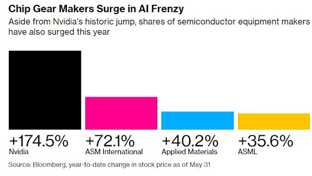
ASM's CEO, Benjamin Loh, highlighted the increasing need for memory in the coming years, particularly in the context of AI technologies. ASM expects the chip market to recover from next year onwards, with sales in 2025 surpassing those of 2022. To capitalize on future growth, ASM plans to invest $100 million in expanding its research operations and facility in South Korea and aims to hire an additional 200 staff within three to five years. Despite restrictions on selling advanced chipmaking gear to China, ASM's position as a key machinery provider to Nvidia, a leading AI accelerator supplier, has contributed to its shares gaining over 70% this year.


Loh, reiterates that the company will experience minimal impact from the restrictions on exporting semiconductor equipment to China. Loh mentions that while they are unable to sell the most advanced equipment, there is still a significant market for other non-restricted equipment, and they can continue trading with Chinese customers. He remains optimistic about the future, stating that as long as chip demand continues to grow, there will be other buyers for their premium products. 

Loh also highlights the challenge of complete decoupling between China and the US, as the chip supply chain remains highly globalized. Recent statements from US officials reflect a shift towards derisking rather than decoupling from China in efforts to improve relations between the two economies.

Thursday, February 2, 2023

Dutch ALD euipment leader ASM to invest $100 mil. in Korea for facility expansion

Korea’s industry ministry said Thursday it agreed with Dutch semiconductor equipment supplier ASM to boost cooperation for the firm’s planned investment of $100 million to build a production factory and a research and development center in Korea.


The two sides signed a memorandum of understanding (MOU) in Seoul on the day, which calls for joint work for the smooth implementation of the corporate investment worth $100 million through 2025, according to the Ministry of Trade, Industry and Energy.

The company is reviewing building a second factory that produces equipment for atomic layer deposition, a key process in chips manufacturing, and the expansion of its RD center in Korea.

Currently, ASM is headquartered in the city of Hwaseong, Gyeonggi Province, some 40 kilometers south of Seoul.

In October, ASM announced a plan to invest $100 million in Korea, but the amount has surged “as discussions between the two sides have developed,” a ministry official said.

Following the MOU signing ceremony, Industry Minister Lee Chang-yang and ASM CEO Benjamin Loh held a meeting for discussions on the envisioned expansion of bilateral cooperation.

“The investment is expected to help Korea better ensure stable supply chains of the sector and boost exports,” the ministry said in a release. “The government will actively extend support, such as providing incentives and resolving difficulties.” (Yonhap)


Source: Dutch chip firm ASM to invest $100 mil. in Korea for facility expansion

Monday, December 19, 2022

Thin layers paved the way for ASMI’s success - Outgoing CTO Ivo Raaijmakers explains what atomic layer deposition has brought the semiconductor industry

ASM International played a key role in developing a deposition technique that has saved Moore’s law more than once. Outgoing CTO Ivo Raaijmakers explains what atomic layer deposition has brought the semiconductor industry – and ASMI – and what more is in store.
This vision has come true. The technique that ASMI acquired through Microchemistry – atomic layer deposition (ALD) – has become an integral part of the semiconductor manufacturing process. And that’s just the beginning, according to Raaijmakers. The demands placed on material layers are ever higher – thinner, more uniform, featuring just the right properties – and ALD is the best technique to meet them, the former CTO argues.


Well before ALD had proven itself in the deposition of high-k materials, Raaijmakers was already looking at which applications would follow. On his initiative, ASMI acquired Korean company Genitech in 2004, a specialist in plasma-enhanced ALD technology (PEALD). Plasmas are more reactive than un-ionized gases and therefore can deposit materials at lower temperatures. Because chipmakers often have to deal with strict temperature budgets, PEALD expands the scope of ALD.

Tuesday, October 4, 2022

ASM International has completed the acquisition of Italian Silicon Carbide Equipment Manufacturer LPE S.p.A.

ASM International (Euronext Amsterdam: ASM) today announces that it has completed the acquisition of LPE S.p.A., after having received regulatory approvals.

On July 18, 2022, ASM entered into a definitive agreement under which it would at closing acquire all of the outstanding shares of LPE, an Italian based manufacturer of epitaxial reactors for silicon carbide (SiC) and silicon. As announced in our press release of July 18, 2022, the transaction is financed with a combination of cash, a conditional earn out, and 631,154 ASM shares (a combination of 580,000 treasury shares and 51,154 newly issued shares).


The acquisition has been completed today, and LPE is now a fully owned subsidiary and will operate as a product unit under ASM’s Global Products organization.

“This is an important milestone for ASM. We are excited to welcome LPE and its talented and experienced team into ASM,” said Benjamin Loh, President and CEO of ASM. “Together with LPE we look forward to capturing many of the opportunities in the high-growth silicon carbide epitaxy market and to support our power electronics customers with innovative solutions, driving the further electrification of the automotive industry.”
“I believe ASM is the right partner for LPE, especially now looking at the growth we are seeing in the silicon carbide market. The global reach that ASM has with its entrenched supplier and customer networks will bring benefits to all stakeholders,” said Franco Preti, who envisioned the silicon carbide opportunity in the earliest stages and led LPE growth as CEO until the acquisition.

LPE is profitable with margins in line with ASM’s 2021-2025 target model. As announced earlier, LPE’s revenue is projected to grow to more than €100 million in 2023, mainly driven by its SiC epitaxy equipment business. Based on ASM internal estimates, demand for SiC epitaxy equipment is forecasted to grow at a CAGR in excess of 25% from 2021 to 2025, driven by the rapidly expanding market for electric vehicles.

Saturday, September 3, 2022

ASM reports that the ALD market is expected to grow by a CAGR of 16%-20% from 2020 to 2025

ASM International presented its Q2/2022 report in July and a new record orders of EUR 943 million driven by robust new node spending in logic/foundry and by recent wins in memory, particularly for ALD gap-fill in 3D-NAND and continued adoption of HKMG in DRAM.


ASM focuses on the single wafer market so the numbers presented does typically not include ALD Large Batch, which is dominated by Tokyo Electron and Kokusai. Back in 1999, ASM acquired Finnish legendary ALD company Microchemistry and its Pulsar 2000 cross-flow chamber ALD technology, which later took the market as the 300 mm version Pulsar 3000 for HfO2 in HKMG at Intel, TSMC, Samsung Globalfoundries, and others. Now it is interesting to follow how the success story continues also for DRAM HKMG. Since then, ASM has added PEALD from Genitech (South Korea) and Large Batch ALD (A412), and many other ALD process technologies. See recent announcements 2022 here:


So it is interesting that ASM has launched a new ALD Batch platform based on the now rather old A412 and the new TENZA to capture growth in Gap-fill - a stronghold for Lam Research.

The ALD market is driven by increased wafer starts in 300 mm for sub 45 nm nodes, 3DNAND and DRAM, and the ongoing fab expansions world-wide.


  • TechInsights expects WFE to increase by 21% in 2022 (July 2022)
  • Strongest growth in leading-edge nodes, spending on 7nm and below expected to grow from ~25% of WFE in 2020 to ~42% of WFE in 2025
  • Gartner expects total WFE to increase by 19% in 2022 (July 2022)
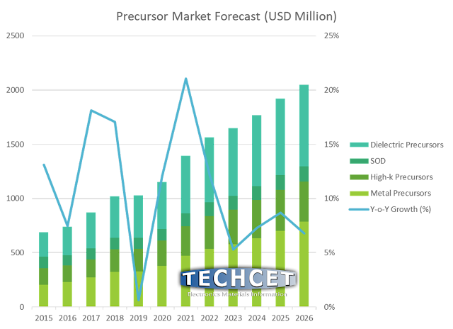
You can compare the TECHCET forecast on precursors where you can see high y-o-y growth going through 2021 and 2023 driven by increased 300 mm wafer production and a slowdown in 2023. Please find deeper dives, assessments and all the data in the TECHCET CMR reports: ALD / CVD Precursors (2) Archives - TECHCET CA LLC


Precursor market forecast 2022-2026 - Invited talk for TECHCET LLC CA in: AA2-TuM2-1 High ALD Equipment and Precursor Demand and 5-Year Forecast Due to Continued Semiconductor Device Scaling and Fab Expansions by Jonas Sundqvist.


Friday, July 15, 2022

ASM International launches TENZA ALD Quad Chambers for silicon oxide gap-fill and liners on the XP8 platform

New process technology addresses 300mm advanced memory and logic/foundry applications with best film quality, highest productivity and lowest cost of ownership in its class.

San Francisco, USA – ASM International N.V. (Euronext Amsterdam: ASM) today announced TENZATM ALD, an innovative single wafer atomic layer deposition (ALD) process technology for 300mm wafers. TENZATM ALD is optimized for gap-fill applications and provides the best film quality, conformal coverage through the full trench and highest productivity in its class.

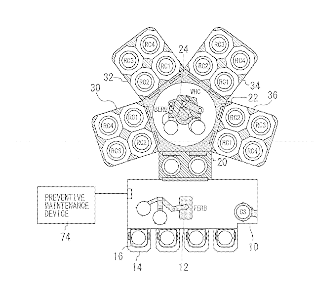
Quad chamber modules (QCMs) 30, 32, 34, and 36 are connected to four side surfaces of the vacuum chamber 22. Each QCM is a module having four reactor chambers (RC1 to RC4). Processing such as plasma film forming processing is performed on a substrate in each reactor chamber. (ASM Patent application US20170278074A1) LINK: BALD Engineering - Born in Finland, Born to ALD: ASM International enhances ALD productivity with new 300 mm XP8 Quad Chamber Module

TENZATM ALD is offered on ASM’s high productivity quad chamber module (QCM) architecture, with four tightly integrated reactors on each QCM. In a compact configuration, up to 4 QCMs running the TENZATM ALD process can be attached to the XP8 platform, enabling processing of up to 16 wafers at a time.

“TENZATM ALD leverages ASM’s production proven QCM quad chamber module architecture and XP8® platform, which have been in high volume manufacturing fabs for several years, to bring enhanced process capability at the lowest cost of ownership to the market. TENZATM ALD enables ultra-high aspect ratio (>100:1) gap-fill for advanced memory devices”, said Hichem M’Saad, Chief Technology Officer and Member of the Management Board.

TENZATM ALD utilizes a novel design optimized for ALD reactions, minimizing process volume for maximum precursor utilization efficiency, reducing precursor consumption up to 50% and increasing productivity more than double compared to conventional ALD approaches. Each reactor chamber controls the RF plasma power supply and matching system individually to improve process reproducibility. The small volume reactor also provides excellent defect performance and extended reactor life (run time before preventive maintenance). Process reactions are confined within each small volume reactor space to minimize consumable parts, making maintenance very easy and less costly.

TENZATM ALD enables a variety of silicon oxide applications for gap-fill and liners for a range of structures in advanced transistors, memory devices and interconnects. The industry can count on TENZATM ALD to deliver a high quality, reliable, repeatable, production proven gap-fill process with the lowest cost of ownership on the market today.

Deliveries of TENZATM ALD have begun to multiple global customers, among them leaders in memory device manufacturing. ASM’s mature compact ALD quad chamber module architecture has a proven track record with more than 2,000 reactors shipped to customers.

Tuesday, July 12, 2022

ASM Internaltional launces new 300 mm Vertical batch for LPCVD and ALD

New system addresses 300mm advanced logic/foundry and memory applications with highest productivity and lowest cost of ownership in its class

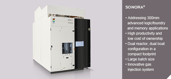
San Francisco, USA – ASM International N.V. (Euronext Amsterdam: ASM) today introduced the SONORA® vertical furnace system with dual reactor chambers for 300mm wafers. The system’s dual boat reactors produce the highest available throughput in its class, increasing reactor utilization to virtually 100%, while ensuring the lowest capex.


SONORA is named after the blossoming Sonoran desert near Phoenix, Arizona. The look and feel of the SONORA system reflects the colors of the Saturn rockets from the Space Age - a time when semiconductor technology was given a huge boost. It is also the era that gave birth to ASM, and so the SONORA® color scheme creates a link to ASM’s more than 50-year legacy in semiconductor processing equipment. LINK: SONORA_vertical_furnace (asm.com)

“The introduction of the novel SONORA® system is part of our strategy to selectively grow our vertical furnace presence in the market. The new SONORA® ensures that ASM will be strengthening its offering in advanced logic/foundry and memory applications as well as extend our leadership position in the market for More than Moore (such as analog and power) applications,” said Hichem M’Saad, Chief Technology Officer and Member of the Management Board.

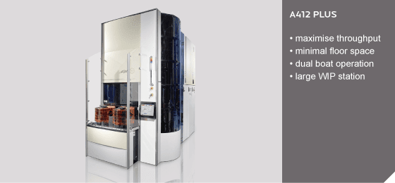
The new SONORA® is fully compatible with the original A412™, so existing process recipes are easily transferred, accelerating system qualification and ramp up. System deliveries have begun to multiple customers globally, among them leaders in advanced logic, and power device manufacturing.

ASM’s predecessor A412™ vertical furnace system has a proven track record of more than 1,000 reactors shipped to customers worldwide and over 22 years of maturity in semiconductor manufacturing. The new SONORA® has a novel system architecture that maximizes floor space productivity as well as service area. Its dedicated process modules have individually controlled high purity mini environments. Our innovative gas injection system for low pressure processing provides the best uniformities of deposited films between the individual wafers at larger load sizes. These larger process wafer load sizes combined with the updated control system, new robots, faster wafer cooldown, faster boat exchange modules generate up to 30% more productivity, compared to its predecessor. Higher productivity also results in lower energy and chemical usage per wafer. Special attention was given to the design for serviceability leading to a spacious access for all maintenance activities. The new system has been further modernized with an intuitive graphical user interface, predictive maintenance by advanced control diagnostics, and plug & play installation. Customers can count on the SONORA® delivering increased reliability and better ease of use with production output that achieves better repeatability, productivity, and time utilization.


The A412 PLUS is for 300mm wafers, while the A400 is for 200mm and smaller wafers sizes

Like its predecessor, the SONORA® offers a comprehensive portfolio of process applications including low pressure chemical vapor deposition (LPCVD) processes like doped silicon and silicon nitride films, diffusion processes such as wet oxidation and anneal processes, as well as a leading portfolio of atomic layer deposition (ALD) materials.

Wednesday, April 6, 2022

Senior Process Engineer I- Coating at ASM Phoenix AZ

About the job

We’re not like most. We don’t just overcome obstacles – we don’t see them. Instead, we see the potential in every person, and every situation. We don’t wait for opportunity to appear – we create it. Meet ASM. A company that has been searching for people just like you.


Job link: (21) Snr Process Engineer I- Coating | ASM | LinkedIn

Who is ASM?

ASM is a leading, global supplier of semiconductor wafer processing equipment. Our ambitious team is dedicated to delivering innovative technology solutions to the world’s leading semiconductor manufacturers. We have over 2,600 employees based in 14 countries, including Belgium, Japan, Netherlands, South Korea, Singapore, Taiwan and United States. Together we work to develop Epitaxy, ALD, PEALD, Vertical Furnaces and PECVD thin-film deposition technologies for our customers. Our goal is to remain an industry leader by being ahead of what’s next. We accomplish this by focusing on finding collaborative solutions to make integrated circuits, or chips, smaller, faster and even more powerful.

ASM, an inclusive workplace

We at ASM are a truly global organization that works diligently with an open-mind in all areas of our business. We strive for a culture and work style that fosters trust and transparency. We put our people first, and that is how we will continue to succeed. We are an equal opportunity employer and value diversity. We recognize and value the differences between individuals, including gender, ethnicity, religious beliefs, sexual orientation, knowledge and experience, work background, age, skills, amongst others. Recruiting and developing a diverse workforce provides a wide range of perspectives. This enables a culture of continuously exploring and adopting new technological ideas and innovations, and it also enables us to deliver excellent products and service to our clients.

Essential Functions
  • Work with a safety-first mentality
  • Drive ASM process protocol with emphasis and regularly institute or update service solutions to the field
  • Work on assigned CIP projects, develop DOE’s and communicate openly both internally and externally.
  • Focus on refresh of IP for legacy products and influence new design IP.
  • Provide “novelty” to items making them hard to reproduce
  • Improve upon existing design for performance and cost efficiency
  • Generate project scope documentation and prepares specific project reports against identified schedule.
  • Building stakeholder consensus to deliver approach
  • Collaboratively manages global stakeholders including end users, technicians, engineers, procurement, spares, manufacturing, subject matter experts as well as management in both business and / or operations to project specific details.
  • Applies project management principles to produce cooperative and collaborative efforts, deliver business strategic objectives and fill the end customer needs.
  • Consistently provide quality solutions to field and customer personnel and create new BKM’s.
  • Exercise good judgment within broadly defined practices and policies in selecting methods, techniques, tools and evaluation criteria for obtaining desired results
  • Be willing to travel domestically and internationally as required.

Education /Experience
  • BS or MS Degree in Mechanical engineering, Electrical Engineering, Material Science or related degree required.
  • 5+ years of experience in the semiconductor field.
  • Equipment Engineering experience with design, and development of complex mechanical systems including comprehension of: reactors, vacuum systems and chambers, gas delivery systems, abatement systems, pneumatics, water cooling, and circuits required. Ability to implement, maintain, improve electrical instruments, equipment, facilities, components, products, systems and provide novel solutions for the semiconductor equipment industry. Comprehension of PLC's and functionality.
  • Should have a broad based background in analysis and debug of complex electrical and/or mechanical systems
  • Semiconductor capital equipment experience is preferred.
  • Understanding of materials: metals, plastics, surface coatings and surface finishes.
  • Deposition product knowledge a plus (CVD, ALD, EPI, PVD). Knowledge of ASM Emerald tool distinct plus.
  • Design applications Pro/ENGINEER, AutoCAD, and Hands on experience with FEA and CFD analysis preferred. Solid ability to read and understand P&IDs, Electrical, and Mechanical schematics and drawings.
  • Proficiency in ANSI Y14.5 geometric dimension and tolerance.

Skills
  • Ability to rectify a challenging situation and gain customer (Internal and external) confidence
  • Strong positive attitude, ability to work in a team environment and work alone. Able to drive meetings, both internal and external, with excellent internal ASM relations
  • Ability to work responsibly with all ASM resources and departments in a multifunctional high paced atmosphere with minimum supervision on highly complex problems
  • Ability to handle multiple tasks simultaneously and be able to organize and run projects
  • Strong computer skills, working knowledge of MS Word, Excel, PowerPoint, SharePoint, Project, and SAP
  • Drive ASM SOP’s and protocol, able to guide co-workers toward common goals
  • Become an active member of ASM GSS core teams
  • Excellent communication skills; speak and write in a clear and concise manner, and ability to accurately and fully convey issues to peers, management, or customers
  • Strong organizational skills and leadership qualities
  • Accurate, timely reporting
  • Parts tracking, ordering, managing, Setting BOM levels
  • Technical writing background. Ability to create procedures, written in an informative manner that eliminates ambiguity and personal interpretation
  • Training skills, be able to communicate with customers and their employees on maintenance procedures, preventative maintenance, and operating specific equipment. Be the content expert with ability to provide onsite support when needed
  • Process comprehension, be able to understand basics of creating process recipes focusing on the ALD process.
  • Understanding of chemistry interactions with different materials. Gas and liquid chemistry knowledge is a bonus
  • Experience with Equipment installs Organizing/Coordinating trades, SL1, SL2, commissioning and qualifications to specific standards.
  • SPC creation with JMP/Statistical analysis and ability to drive root cause solutions through data driven decisions

From the very start of the semiconductor industry to the present day, we’ve been technology leaders who have pioneered innovation and brought new processes into mainstream manufacturing. We are collaborating, creating, and delivering on our vision – a shared vision to drive innovation with new technologies and delivering excellence with dependable products. By doing this, we’ll create new possibilities for everyone to understand, create and share more of what they love.

Be part of our exciting future and join our team today!

Saturday, February 26, 2022

ALD centre of excellence to drive leading edge process technology - ASM International and University of Helsinki have renewed and expanded their long-term research agreement

The new five-year agreement entails a significant expansion of the collaboration that already began in 2004 and now gets extended to the impressive length of 23 years. ASM will more than double the current funding provided to the University as part of this agreement. The accelerator laboratory of Department of Physics receives part of the funding. ASM also plans to expand the team at its subsidiary ASM Microchemistry Oy at the Kumpula campus.

ASM Microchemistry has been pioneering ALD (Atomic Layer Deposition) technology since its founding in 1987 and has been co-located since 2004 in the Chemicum building at the Kumpula campus. University of Helsinki, working on ALD since 1990, hosts HelsinkiALD that is one of the world's best known academic research groups in the field of ALD chemistry. The ALD CoE will focus on ALD and other atomic layer processes and thin film materials that are necessary for future microelectronics. ALD is an advanced technology for depositing thin film materials in highly controlled manner for integrated circuits and other applications. Semiconductors in all today’s mobile phones and computers contain materials made by ALD. One recognition of the importance of the ALD technology was the Millennium Technology Prize that was awarded in 2018 to Dr. Tuomo Suntola, the Finnish inventor of ALD.


In front ASM International CEO Benjamin Loh and vice rector Paula Eerola. Behind from left emeritus prof. Markku Leskelä, CTO and Corporate VP R&D Ivo Raaijmakers, VP of Technology & Corporate R&D Vamsi Paruchuri, prof. Mikko Ritala, Senior Director Corporate R&D Operations Kees van der Jeugd, dean Kai Nordlund and assistant prof. Matti Putkonen. (Image: Jani Närhi)

Benjamin Loh, CEO of ASM International, commented:

– The ALD Center of Excellence agreement significantly expands our nearly two-decade long and successful collaboration with University of Helsinki. We are very excited about this partnership aimed for breakthroughs around ALD that will enable future semiconductor technologies.

– Collaboration with ASM, which is exceptional in terms of both length and volume, is highly valuable for the University of Helsinki, stated vice-rector Paula Eerola.

Professor Mikko Ritala and associate professor Matti Putkonen who head the HelsinkiALD research group at the University added:

– We greatly appreciate ASM for the long-term commitment and collaboration. Our research area is clearly exceptionally fruitful and rewarding for academia-industry collaboration. The research questions we are addressing are fundamental by their nature, yet our results may find immediate use in the future semiconductor devices. Therefore division between basic and applied research is meaningless.

A critical element behind the successful collaboration is the mutual understanding and respect of each party’s interests, in particular intellectual property protection for ASM and open science for the university.

– When new innovations are made, these are first patented, after which we are free to publish all the results without any undue delay, said Ritala.

In 2020 ALD center Finland research infrastructure, formed by HelsinkiALD in chemistry department and accelerator and x-ray physics laboratories in physics department, was selected by Academy of Finland to the national research infrastructure roadmap. ALD center Finland serves as a national platform for research and education in atomic layer level processing techniques. The center also supports other fields of research requiring state-of-the-art techniques for thin film deposition, characterisation and surface chemistry, catalysis in particular.

ALD research has also a strong educational dimension.

– It is a pleasure seeing how wanted chemists graduating from us are in the industry and elsewhere. To make the training even more attractive, a unique Master´s programme in ALD has been launched. The students will be majoring from Inorganic materials chemistry study track of Master’s Programme in Materials Research, and their courses are directed so that they cover all important aspects of ALD, including precursors, thin film deposition and characterization as well as potential applications, explains Matti Putkonen, who was appointed in 2019 as an associate professor in atomic layer deposition and etching, seemingly the first one of its kind in the world.

– Our education and hands on training create an exceptionally good starting point for our graduates to become part of the rapidly increasing global ALD community.

Saturday, October 2, 2021

ASM International Investor Day take away - the leader in ALD wafer processing equipment for the booming semiconductor industry

 ASM International, the leader in ALD wafer processing equipment for the booming semiconductor industry recently hold its annual investor day.

Highlights included:
  • Targeting revenue of €2.8-€3.4 billion by 2025 (2020-2025 CAGR of 16%-21%), gross margins of 46%-50% in 2021-2025, and operating margins of 26%-31% in 2021-2025;
  • Targeting Net Zero emissions by 2035 and 100% renewable electricity by 2024;1
  • Single-wafer ALD market expected to increase from $1.5 billion in 2020 to $3.1-3.7 billion by 2025;
  • Further capacity expansion of our new manufacturing facility to be production ready by early 2023.

3D device architecture evolution is continuing into all leading-edge semiconductor components. 3DNAND and FinFET are to be followed by GAA FETs and 3D-DRAM. Together with the need for new materials drives the demand for CVD and ALD processing equipment (ASM Investor Day 2021)

“I’m very excited to share the strong prospects for our company during our first Investor Day,” said Benjamin Loh, CEO of ASM International. “We project revenue to increase to €2.8–€3.4 billion by 2025, with operating margins of 26%-31% during the 2021-2025 period. Key inflections in next generation semiconductor devices such as complex 3D architectures and new materials, are expected to drive double digit growth in ASM’s key markets. Today we will also highlight new innovations in our products, enabling our customers’ technology roadmaps. Capitalizing on our innovative strength, early customer engagements and product differentiation, we are focused on maintaining our leading position in the ALD market and to further increase our market share in Epi.


The semiconductor market, historical and as forecasted by VLSI Research. By 2030 it will have doubled to USD 1 Trillion. (VLSI Research - ASM Investor Day 2021)

In view of the strong growth opportunities ahead of us we will further step up our R&D investments and strengthen our capabilities. In addition, with our new expanded manufacturing facility in Singapore completed just less than one year ago, we have now decided to prepare a further substantial capacity increase within this facility to be production ready by early 2023.


The Wafer Equipment market growth has reached a new level and will sustain it for years to come (VLSI Research - ASM Investor Day 2021).


ASM controls more than 50% of the single wafer ALD equipment market and intends to defend the market share going forward to 2025. The market is forecasted by ASM to more than double 2020 to 2025, reaching USD 3.1 to 3.7 billion by then. (ASM Investor Day 2021)

A further increase in our ambition to sustainability is a central element in our strategy. As an important next step we announce today our ambitious target to achieve Net Zero emissions by 2035 (scope 1, 2 and 3) and 100% renewable electricity by 2024. As we continue to drive growth through innovation, ASM is well positioned to create long-term value for all its stakeholders.”


ASM Roadmap for DRAM, 3D-NAND and Logic,  aligned with its leading-edge customer base. (ASM Investor Day 2021)

The Investor Day was held at 2:00 pm CET  and Q&A can also be followed through a live webcast after registering at: https://investorday.asm.com.

Presentation:LINK

UPDATE Q3 2021 GUIDANCE

ASM also announced that Q3 order intake is expected to be above €600 million, compared to previous guidance of €510-530 million, mainly driven by continued strong demand in the logic/foundry sector. Q3 net sales are expected to be in line with previous guidance €400-430 million.

Thursday, May 27, 2021

Atomic billiards helps to understand Atomic Layer Deposition

In the beautiful German city of Münster, scientists are playing games on an atomic scale to help ALD developers understand what is going on in their process. Critical ALD parameters, such as the evolution of film closure and thickness with increasing cycle number are determined with a game of billiards at the atomic level. This game is called LEIS (Low Energy Ion Scattering), the most surface specific chemical analysis technique available to the surface scientist.

The fundamental principles behind LEIS are surprisingly simple: In an ultrahigh vacuum chamber, light charged particles (ions) are aimed at the sample where they collide with the atoms in and on the sample. These collisions obey the same laws of physics as collisions between large objects, such as balls. This means that the ions are bouncing (or scattering) back with high speed (or energy) when they collide with a heavy atom and with low energy after a collision with a light atom. The energy of the scattered ions is measured to determine the mass of the surface atoms.

Figure 1: The principle of LEIS: When ions collide with surface atoms, their energy after the collision depends on the mass of the atoms that they collided with. A LEIS spectrum shows the number of returned ions as a function of their energy. This represents the surface concentrations of different elements, sorted after their mass.

LEIS helps to develop and optimize ALD processes


We show an example of a co-operation between scientists at Tascon in Münster and the ALD experts from ASM Microchemistry Oy in Helsinki, Finland where the initial formation of a GaSb film on SiOx was investigated.

Figure 2 shows a set of LEIS spectra for the increasing number of ALD cycles recorded with Neon ions. There are two peaks due to collisions with Gallium (Ga) and Antimony (Sb) atoms in the outermost atomic layer of these samples. Antimony atoms are heavier than Gallium atoms and therefore the peak from collisions with Antimony lies at higher energy than the Gallium peak.


Figure 2: 5 keV 20Ne+ LEIS spectra of increasing cycle numbers of GaSb deposited on SiOx
As one would expect, the amount of Gallium in the outermost atomic layer is increasing continuously with increasing cycle number (from red to purple) showing how the fraction of Gallium increases in the outermost atomic layer. The Antimony behaves differently, though. After increasing initially, its signal goes through a maximum (the green spectrum), and with increasing cycle number the amount of Antimony at the surface decreases. With this valuable information, the ALD expert can optimize the deposition process.

LEIS separately analyzes the outermost atomic layer and the layers below it

As we have seen, LEIS is sensitive to the outermost atomic layer of a sample. The used noble gas ions (Helium or Neon) lose their charge as soon as they enter the material. Since the instrument can only detect ions, the neutral Helium or Neon atoms that collided in deeper layers are not detected. Therefore, the peaks in the spectrum from figure 2 represent Gallium and Antimony at the surface.

Particularly when Helium ions are used, there is a second effect. A Helium atom, that collided in deeper layers, may lose an electron as it leaves the surface. The probability for this re-ionization is small enough to recognize the peaks in the spectra, but large enough to cause an additional signal in the spectrum, as shown in figure 3, a set of spectra recorded with Helium ions from the same GaSb deposition study.

Figure 3: 7 keV 4He+ LEIS spectra of increasing cycle numbers of GaSb deposited on SiOx.
Again, we see the Gallium peak increasing and the Antimony peak going through a maximum. This time, we also see the Silicon (Si) peak decreasing with increasing cycle number, confirming that the substrate is getting covered. But we also see that with increasing cycle number shoulders appear on the left side of the Gallium and Antimony peaks (indicated by the dashed arrows).

These shoulders are caused by collisions from Gallium and Antimony atoms below the surface. The Helium atoms have slowed down while traveling through the sample on their way to and from the colliding atom. The more the shoulder extends to lower energy, the more the atoms have slowed down and the deeper the colliding atom was in the sample. The fact that the shoulders are extending more and more to the left with increasing cycle number shows that the film is getting thicker.

Since LEIS is a quantitative analysis technique, the surface fractions can be determined from the spectra. Figure 4 shows a ternary diagram for the composition of the sample surface with increasing cycle number. It clearly shows that initially Gallium and Antimony are deposited together. But as the film is almost closed, the Gallium deposition starts to dominate.


Figure 4: Ternary diagram showing the surface composition of the samples with increasing cycle number. The colors of the data points correspond to the colors of the spectra.
This example shows the value of LEIS in the study of ALD. Because of its surface specificity and the need for ever thinner films, the role of LEIS in ALD is expected to increase in the coming years.

Acknowledgement

The GaSb films in this study were kindly provided by ASM Microchemistry Oy, Helsinki, Finland.

Guest blog by Rik ter Veen and Karsten Lamann, Tascon GmbH, Münster, Germany

About the authors:

Rik ter Veen and Karsten Lamann are scientists at Tascon GmbH, a service provider and consulting company for the analysis of surfaces, films and interface for over 20 years with two locations in Germany and one in the USA. In addition to LEIS, the subject of this blog, Tascon offers surface and materials analysis with techniques such as ToF-SIMS, XPS and SEM-EDX. If you are interested in their services or have questions about LEIS, or other techniques, the authors can be contacted through their website.

Wednesday, April 21, 2021

ASM International and ALD opens up 2021 with a strong quarter in Logic & Foundry segment

ASM International N.V. (Euronext Amsterdam: ASM) today reports its first quarter 2021 operating results (unaudited) in accordance with IFRS.

  • New orders at €411 million were 8% above the level of last quarter.
  • Revenue for the first quarter of 2021 was €394 million and increased 14% compared to the previous quarter due to strong market demand.
  • The gross profit margin was 49.5% in Q1 2021 compared to 45.2% in the previous quarter, mainly due to a favorable mix.
  • The operating result was €125 million compared to €78 million in the previous quarter.
  • Normalized net earnings for the first quarter of 2021 were €125 million, €43 million higher compared to Q4 2020.
LINKS
Q12021 Presentation: LINK
Earings Call Transcript (Seeking Alpha): LINK
  • Gartner expects WFE to increase by 23% in 2021 (April 2021), up from +8% still predicted in December 2020
  • VLSI Research expects WFE to increase by 22% in 2021 (April ’21), up from a previous forecast of +12% last February

“2021 started very strong for ASM,” said Benjamin Loh, President and Chief Executive Officer of ASM International. “In the first quarter, we realized revenue of €394 million, well within our guidance of €380-400 million and up 14% from the level in Q4. The revenue level was again driven by continuous high demand in the logic/foundry segment. Our Q1 order intake, at €411 million, was up 8% from an already high level in Q4 and ahead of our guidance of €380-400 million, driven by solid demand in logic/foundry. Our gross margin was at a high level of 49.5%, caused by a favorable mix, while our operational cash flow showed a record high level in Q1. Based upon the strong cash position at the end of March, we plan to start a new €100 million share buyback program.”

Outlook

For Q2, on a currency comparable level, we expect revenue of €390-€410 million. Q2 bookings, on a currency comparable level, are expected to be in the range of €420-€440 million.

“Based upon the current market developments, the wafer fab equipment (WFE) market is expected to grow by a high-teens to low twenties percentage in 2021.”

Based upon the current market developments, the wafer fab equipment (WFE) market is expected to grow by a high-teens to low twenties percentage in 2021. 2021 is expected to develop in another year of solid growth for ASM. Based upon our current view, we expect our sales in the second half to be at least at the same level as in the first half.

ALD and New Market segment

"Moving to the longer-term outlook, ALD continues to be an important, long-term growth market for ASM. For 2020, we estimate the single wafer ALD market, to reach the size of US$1.5 billion in line with the expectations we put out several years ago. We are currently reviewing our focus and expect to present the new market for customers later in the year. However, it is clear to us that ALD will remain the fastest-growing segment of the deposition market, with substantial, double-digit growth potential in the coming years. ALD is a critical technology for our industry to develop the next generation's faster processes and memory devices that in turn will enable the growth of key markets such as in 5G and artificial intelligence." - Benjamin Loh

DRAM and High-k/Metal Gate adaption with ALD

ASM's recent most significant achievement in expanding our memory presence has been in ALD wins for high-k metal gate in the high-performance DRAM segment, with the leading memory players. It is a key technology that reduces device leakage and thereby supports increases in both energy efficiency and device performance. As reported earlier, ASM books their first meaningful sales for this application last year and expects it to support a healthy increase in our DRAM sales this year.

What has been launched today is primarily what is called the high-performance DRAM segment or sub-segment within the DRAM market and it has been adopted by all the DRAM manufacturers.

ASM ALD Market Share

According to the information given in the call, Gartner report ASM´s market share in the single wafer ALD market has grown from 57% to 60% during 2020 and Benjamin Loh agreed that that estimate is in the right direction. 


Friday, March 26, 2021

Samsung confirms first HKMG for DDR5 DRAM

ASM International recently acknowledged that ALD High-k/Metal Gate (HKMG) is finally in high volume production for DRAM (LINK). Now Samsung confirms that. This is a small victory for all people working on this process for such a long time. My first tool ownership when I moved to Germany and started at Infineon was an ASM Polygon 200 mm cluster with a Pulsar 2000 chamber running HfO2, TiN, TiHfN, TiAlN, Al2O3, and my not fully understood HfN ALD process and a Poly chamber that I never really cared too much about. Press release below - and now do the maths - how big this business is once rolled out for all DRAM technologies to come - yeah $$$, many tulips indeed.


Samsung Develops Industry’s First HKMG-Based DDR5 Memory; Ideal for Bandwidth-Intensive Advanced Computing Applications

512GB capacity DDR5 module made possible by an 8-layer TSV structure
HKMG material reduces power by 13 percent while doubling the speed of DDR4


Samsung Electronics, the world leader in advanced memory technology, today announced that it has expanded its DDR5 DRAM memory portfolio with the industry’s first 512GB DDR5 module based on High-K Metal Gate (HKMG) process technology. Delivering more than twice the performance of DDR4 at up to 7,200 megabits per second (Mbps), the new DDR5 will be capable of orchestrating the most extreme compute-hungry, high-bandwidth workloads in supercomputing, artificial intelligence (AI) and machine learning (ML), as well as data analytics applications.


“Samsung is the only semiconductor company with logic and memory capabilities and the expertise to incorporate HKMG cutting-edge logic technology into memory product development,” said Young-Soo Sohn, Vice President of the DRAM Memory Planning/Enabling Group at Samsung Electronics. “By bringing this type of process innovation to DRAM manufacturing, we are able to offer our customers high-performance, yet energy-efficient memory solutions to power the computers needed for medical research, financial markets, autonomous driving, smart cities and beyond.”

“As the amount of data to be moved, stored and processed increases exponentially, the transition to DDR5 comes at a critical inflection point for cloud datacenters, networks and edge deployments,” said Carolyn Duran, Vice President and GM of Memory and IO Technology at Intel. “Intel’s engineering teams closely partner with memory leaders like Samsung to deliver fast, power-efficient DDR5 memory that is performance-optimized and compatible with our upcoming Intel Xeon Scalable processors, code-named Sapphire Rapids.”

Samsung’s DDR5 will utilize highly advanced HKMG technology that has been traditionally used in logic semiconductors. With continued scaling down of DRAM structures, the insulation layer has thinned, leading to a higher leakage current. By replacing the insulator with HKMG material, Samsung’s DDR5 will be able to reduce the leakage and reach new heights in performance. This new memory will also use approximately 13% less power, making it especially suitable for datacenters where energy efficiency is becoming increasingly critical.

The HKMG process was adopted in Samsung’s GDDR6 memory in 2018 for the first time in the industry. By expanding its use in DDR5, Samsung is further solidifying its leadership in next-generation DRAM technology.

Leveraging through-silicon via (TSV) technology, Samsung’s DDR5 stacks eight layers of 16Gb DRAM chips to offer the largest capacity of 512GB. TSV was first utilized in DRAM in 2014 when Samsung introduced server modules with capacities up to 256GB.

Samsung is currently sampling different variations of its DDR5 memory product family to customers for verification and, ultimately, certification with their leading-edge products to accelerate AI/ML, exascale computing, analytics, networking, and other data-intensive workloads