Friday, December 23, 2022

Picosun initiates R&D program in Finland for sustainable semiconductor manufacturing

ESPOO, Finland, 22nd of December 2022 – Picosun, an Applied Materials company, has received funding from Business Finland to form an R&D program in the country focused on reducing the environmental impact of semiconductor manufacturing.

The four-year program, called “Chip Zero,” seeks to bring together companies across the semiconductor ecosystem in Finland with a shared mission of developing chips with zero lifetime emissions by reducing the carbon footprint of chip manufacturing and increasing the efficiency of semiconductor decarbonization applications. Picosun will initiate and lead the program with a significant grant from Business Finland. The aim is to scale the program over time with contributions from ecosystem partners to reach more than 100M€ in R&D investments.


Photo, Björn Engström, Oravais, Ostrobothnia, Finland.

Chip Zero will include efforts to reduce energy consumption and the environmental impact of chemical use in semiconductor manufacturing. Specific goals include achieving a 50-percent reduction in energy and chemical consumption of thin-film deposition and a double-digit increase in the efficiency of power electronic component applications, such as electric vehicle (EV) chargers and electric motor control electronics, by 2030. Among the strategies to achieve these goals is the development of optimized process flows for chip manufacturing.

“Picosun is excited to lead the Chip Zero program and bring together Finland’s strong technology R&D ecosystem with a common objective of developing more efficient chips and minimizing the environmental impact of manufacturing. We look forward to collaborating across the value chain to drive critical advances that will accelerate a greener and more sustainable semiconductor industry in Finland,” says Dr. Jani Kivioja, CTO of Picosun.

“With the global semiconductor market projected to reach US$1 trillion by 2030*, the need for greater efficiency in chip manufacturing is more important than ever. Finland has significant and pioneering competences in key chipmaking technologies, and the Chip Zero program intends to focus these capabilities on strengthening the country’s sustainability efforts,” continues Jussi Rautee, CEO of Picosun and Vice President of Applied Materials.

“The opportunity for technology to shape a more sustainable world has never been more promising,” says Chris Librie, Applied Materials Director of ESG, Corporate Sustainability and Reporting. “At Applied Materials, our vision is to Make Possible a Better Future, and we are pleased that our team in Finland is making a positive difference through programs like Chip Zero that aim to reduce the environmental impact of computing.”


Thursday, December 22, 2022

SparkNano's Spatial ALD tool decreases the of Iridium while increasing the production capacity of electrolyzers for green hydrogen

SparkNano's Spatial ALD tool decreases the cost and use of scarce materials like Iridium while increasing the production capacity of electrolyzers for green hydrogen.

For more detail about SparkNanos lab-to-fab product portfolio, you can download the complete spec sheet for the Labline Series here: LabLine Series — SparkNano | Spatial Atomic Layer Deposition (ALD) technology (spark-nano.com)

Technical features (12 inch system)

Substrate types flat substrates like polymer and metal foils, wafers, glass and porous substrates

Substrate size

A free envelope of 320 mm x 360 mm x 5 mm is available. In this volume any flat substrate can be placed with a substrate specific holder

Process

Both thermal and plasma enhanced s-ALD


Swedish Nanexa signs Evaluation Agreement with and issues a directed shares to Novo Nordisk for ALD based PharmaShell(R)

Nanexa AB (publ) (“Nanexa” or the “Company”) today announces that the Company has signed a Material Transfer and Feasibility Study Agreement (the “Evaluation Agreement”) with leading global pharmaceutical company Novo Nordisk A/S (”Novo Nordisk”) for the evaluation of Nanexa’s drug delivery system PharmaShell® with Novo Nordisk products. As part of the Evaluation Agreement, Nanexa will receive payments of approximately SEK 46.1 million for providing Novo Nordisk exclusivity and performing work under the Evaluation Agreement, whereof approximately SEK 41.7 million is an upfront payment at signing. In connection with the signing of the Evaluation Agreement, the board of directors of Nanexa also resolved, based on the authorisation granted by the annual general meeting held on 9 June 2022, to carry out a directed share issue to Novo Nordisk of 10,000,000 shares at a subscription price of SEK 1.72 per share (the “Directed Share Issue”) through which Nanexa raises gross proceeds of approximately SEK 17.2 million. The subscription price is equivalent to a premium of 33 percent versus the closing price yesterday for the Company’s shares. In total, Nanexa will thus receive approximately SEK 63.3 million from the Evaluation Agreement and the Directed Share Issue.


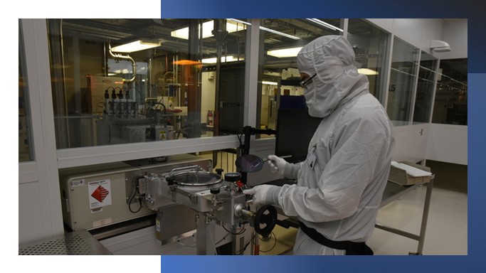
Novo Nordisk is a leading global pharmaceutical company engaged in the research, development, manufacture and commercialization of pharmaceutical products and associated devices for treatment of diabetes, obesity and other diseases. Under the Evaluation Agreement Novo Nordisk will provide Nanexa with its products and Nanexa will develop a long-acting injectable using the PharmaShell® drug delivery system. The new formulation will be evaluated in preclinical studies by Novo Nordisk. As part of the Evaluation Agreement, Nanexa receives a fee of USD 4.0 million for providing Novo Nordisk exclusivity to use PharmaShell® in combination with Novo Nordisk products, valid throughout the term of the exclusivity, and USD 0.425 million for the work performed under the Evaluation Agreement. The combined fees of USD 4.425 million correspond to approximately SEK 46.1 million. Throughout the exclusivity period Novo Nordisk has the option to negotiate a license agreement. Nanexa will be able to continue the development of its own product project (NEX-22) within the field of type 2 diabetes throughout the exclusivity period.

In connection with the signing of the Evaluation Agreement, Novo Nordisk invests SEK 17.2 million in Nanexa in the Directed Share Issue. The Directed Share Issue comprises 10,000,000 shares issued at a subscription price of SEK 1.72 per share. The subscription price is equivalent to a premium of 33 percent versus the closing price for the Company’s shares on Nasdaq First North Growth Market as per yesterday, 20 December 2022 (the “Closing Price”) and a premium of 10 percent versus the volume weighted average price of the last twenty (20) trading days for Nanexa’s shares on Nasdaq First North Growth Market preceding 20 December 2022 (the “20-day VWAP”). Following the Directed Share Issue, Novo Nordisk’s ownership in Nanexa will amount to approximately 16.5 percent of the Company’s shares and votes. The Directed Share Issue results in a dilution of approximately 16.5 percent of the Company’s shares and votes. The number of shares of Nanexa after the Directed Share Issue will amount to 60,695,626 and the share capital of Nanexa will increase by approximately SEK 1,294,213.58 to approximately SEK 7,855,310.32. Additionally, Novo Nordisk undertakes as part of the Directed Share Issue to subscribe for its pro-rata portion of any future rights issue conducted prior to 31 December 2023 up to a maximum of USD 2.0 million. The undertaking is conditional on certain terms being met.

The net proceeds from the Directed Share Issue will primarily be used to strengthen the Company’s financial position, and to enable planned preclinical and clinical studies as well as other value creating activities supporting PharmaShell® and the NEX projects.


The purpose of the Directed Share Issue, and the reason for deviation from the preferential rights of the shareholders, is (i) in a time and cost efficient manner acquire capital and to finance the joint development project between the Company and Novo Nordisk pursuant to the Evaluation Agreement , (ii) to add a strategically important and financially strong shareholder, who wishes to participate in the future development of the Company, to its shareholder base, (iii) that Novo Nordisk will bring valuable industry and sector knowledge to the Company, and (iv) that a rights issue, as opposed to a directed issue, would not ensure that Novo Nordisk actually becomes a shareholder in the event that the rights issue is fully subscribed. The board further believes that it would entail a risk that the Company cannot accommodate the capital needs associated with its business plan at favourable terms in the current market situation. Consequently, the overall assessment of the Board of Directors is that the reasons for carrying out the Directed Share Issue in this way, in this specific case, outweigh the reasons justifying the main rule of issuing shares with preferential rights for existing shareholders, and that a new issue with deviation from the shareholders' pre-emption rights is therefore in the interests of the Company and all shareholders.

The subscription price has been determined through arm's length negotiations between the Company and Novo Nordisk. The subscription price exceeds the Closing Price by 33 percent and the 20-day VWAP by 10 percent. Existing shareholders have therefore had good opportunities to acquire shares on similar or more favourable terms recently. As the subscription price in the Directed Share Issue not insignificantly exceeds both the closing price and the 20-day VWAP, the board of directors considers that it has been ensured that the subscription price is on market terms.

Göran Ando, Chairman of the board, comments:

"I am very pleased that we through the Evaluation agreement and the Directed Share Issue can give Nanexa good conditions to continue developing the Company into a world leading drug development company for long-acting injectables, based on our unique PharmaShell® technology. The collaboration with Novo Nordisk further strengthens Nanexa’s portfolio of partner projects with a good opportunity to develop into a more extensive development program and long-term license agreement. The deviation from the shareholders' pre-emptive rights is not a decision taken lightly, but the possibility to reach a solution under prevailing volatile market conditions with a premium, as well as adding Novo Nordisk as strategic partner, was a strong reason."

Monday, December 19, 2022

Foundations of atomic-level plasma processing in nanoelectronics (Open Access)

Foundations of atomic-level plasma processing in nanoelectronics

Karsten Arts, Satoshi Hamaguchi, Tomoko Ito, Kazuhiro Karahashi, Harm C M Knoops, Adriaan J M Mackus and Wilhelmus M M (Erwin) Kessels
Plasma Sources Sci. Technol. 31 103002 OPEN ACCESS  

This article discusses key elementary surface-reaction processes in state-of-the-art plasma etching and deposition relevant to nanoelectronic device fabrication and presents a concise guide to the forefront of research on plasma-enhanced atomic layer etching (PE-ALE) and plasma-enhanced atomic layer deposition (PE-ALD). As the critical dimensions of semiconductor devices approach the atomic scale, atomic-level precision is required in plasma processing. The development of advanced plasma processes with such accuracy necessitates an in-depth understanding of the surface reaction mechanisms. With this in mind, we first review the basics of reactive ion etching (RIE) and high-aspect-ratio (HAR) etching and we elaborate on the methods of PE-ALE and PE-ALD as surface-controlled processing, as opposed to the conventional flux-controlled processing such as RIE and chemical vapor deposition (CVD). Second, we discuss the surface reaction mechanisms of PE-ALE and PE-ALD and the roles played by incident ions and radicals in their reactions. More specifically, we discuss the role of transport of ions and radicals, including their surface reaction probabilities and ion-energy-dependent threshold effects in processing over HAR features such as deep holes and trenches.


Examples of applications of PE-ALD in patterning, logic device fabrication, and memory device fabrication. The layers prepared by PE-ALD are indicated in (dark) red. In these examples, i.e., self-aligned quadruple patterning (A), gap-filling (B), and dielectric lining (C, left), the film conformality, thickness control, and material quality provided by PE-ALD are essentia

Thin layers paved the way for ASMI’s success - Outgoing CTO Ivo Raaijmakers explains what atomic layer deposition has brought the semiconductor industry

ASM International played a key role in developing a deposition technique that has saved Moore’s law more than once. Outgoing CTO Ivo Raaijmakers explains what atomic layer deposition has brought the semiconductor industry – and ASMI – and what more is in store.
This vision has come true. The technique that ASMI acquired through Microchemistry – atomic layer deposition (ALD) – has become an integral part of the semiconductor manufacturing process. And that’s just the beginning, according to Raaijmakers. The demands placed on material layers are ever higher – thinner, more uniform, featuring just the right properties – and ALD is the best technique to meet them, the former CTO argues.


Well before ALD had proven itself in the deposition of high-k materials, Raaijmakers was already looking at which applications would follow. On his initiative, ASMI acquired Korean company Genitech in 2004, a specialist in plasma-enhanced ALD technology (PEALD). Plasmas are more reactive than un-ionized gases and therefore can deposit materials at lower temperatures. Because chipmakers often have to deal with strict temperature budgets, PEALD expands the scope of ALD.

Saturday, December 17, 2022

ALD Stories Podcasts by Tyler Myers

Message from Tyler Myers to the ALD-Community - The community with a forecasted 5-Year CAGR 20.5% (2022-2026) - Please consider following the ALD Stories podcast! Each month, you'll find insightful interviews about the lives and research of the best folks in ALD. We already have a couple episodes ready to go for 2023!


Here is how I listen to the ALD Stories using my new Sony Head set with 2 processors and 8 microphones for unprecedented noise cancellation and exceptional call and sound quality. Besides that my phone has so many ALD-chips I sort of bet that each chip in the headphones has ALD in them so what better way to deploy ALD technology than to run and listen to ALD Stories using 8 microphones and the advanced speakers to filter out the wind, ugly birds song and traffic and still be able to answer and participate in web meetings?


2023 I will experiment with adding video feed capability.


Kokusai Electric relies on patterned 3D substrates in thin film process metrology from Chipmetrics

Kokusai Electric is one of the leading semiconductor thin film process equipment manufacturers in the world. Recently, in the context of Japan Society of Applied Physics 69th Spring Meeting 2022, Kokusai presented their advanced thin film measurement and analysis concept used in their semiconductor process development.

The concept focuses on film thickness and localized film composition measurements from the special designed 3D patterned substrates, where the patterns are fine high aspect ratio structures.

The average film thickness is obtained indirectly by measuring the mass change in the special 3D patterned wafer before and after the film depositions. The thickness accuracy is further improved by taking into account the high aspect ratio and wafer level non-uniformity measured by PillarHall® Lateral High Aspect Ratio (LHAR) test chips positioned on the carrier wafer. The PillarHall® measurement, enables easy screening after peeling off the top roof membrane and by measuring the film thickness distribution and conformality by the ellipsometer line-scanning measurements.

PillarHall® LHAR test chip has also another important function in Kokusai’s analysis concept. Namely, it is used for film elemental composition characterization along the trench wall in high aspect ratio structure. The measurement is carried out as a line-scan by XPS or SEM-EDS. For example, the characterization showed that two kinds of SiN processes behaved differently and Si/N composition changes along the high aspect ratio (AR>1000) trench were observed.


Figure 1. PillarHall experiment summary


Figure 2. SiN film thickness data


Figure 3. SiN(2) XPS data

Figures 1-3 show the PillarHall experimental set-up, data from the film thickness penetration depth profiles and XPS composition data of two kind of Kokusai’s SiN processes, SiN (1) and SiN (2).

Kenji Kameda and Akane Kitamura from Metrology Team, Kokusai Electric emphasized that:” It is difficult to obtain the analysis of thin films on high aspect ratio patterns without cross-sectional TEM. PillarHall is a simple and effective tool, it has fine patterns, and it enables us to use XPS and ellipsometer instead of TEM. Therefore, PillarHall is useful as an efficient measurement tool to improve Kokusai’s film forming technology.”

PillarHall LHAR test chip is a product of Chipmetrics Ltd, Finland. Chipmetrics CEO Dr. Mikko Utriainen reminds that any PillarHall data can be published without confidentiality concerns and the results are also well comparable between reactor systems and processes. The openness and accuracy of the ALD conformality data was one of the reasons why pioneering ALD scientists in Finland started to develop the PillarHall concept already in 2013.

Kokusai’s example shows that PillarHall is an efficient measurement tool and help to improve film forming technology for advanced semiconductor processes.

PillarHall is a product of Chipmetrics Ltd. Contact: info@chipmetrics, www.chipmetrics.com

Friday, December 16, 2022

MIT.nano adds new instruments to create and analyze at the nanoscale from Arradiance

The Arradiance GEMStar XT-DP plasma-enhanced atomic layer deposition (ALD) system was installed at MIT.nano in May.


The system is dedicated specifically to deposit high-quality nanometer-scale thin oxide films including aluminum oxide, hafnium oxide, zirconium dioxide, and silicon dioxide. The Arradiance ALD can be used for samples ranging from small pieces up to 200-mm wafers and has a load lock that isolates the deposition chamber from the user, allowing for better contamination control.