Friday, November 25, 2022

Applied Materials Delivers Strong FY 2022 Numbers including Picosun ALD

Semiconductor equipment maker Applied Materials has reported strong earnings for FY 2022 (ended October 30). Total sales revenue increased 12% YoY to $25.78 billion despite supply chain shortages, geopolitical and macroeconomic headwinds, and softening consumer demand.

LINK: https://ir.appliedmaterials.com/

The company’s uniquely enabling technology and growing installed base will be its key growth drivers as chipmakers accelerate ramping up of new process nodes in R&D for high-volume manufacturing.


Key developments in FY 2022
  • Applied Materials acquired Picosun, a Finland-based innovator in atomic layer deposition (ALD) technology. This acquisition broadens Applied’s product portfolio and puts it in a great position to capture a large portion of the specialty semiconductor market in the coming years.
  • Collaboration with the Institute of Microelectronics (IME), a research institute under Singapore’s Agency for Science, Technology and Research (A*STAR). IME’s strategic R&D capabilities complement well Applied’s expertise in advanced packaging solutions and will accelerate material, equipment and process technology solutions for hybrid bonding and other emerging, 3D chip integration technologies.
  • Introduced new Ioniq™ PVD system to solve wiring resistance challenges of 2D scaling. This new integrated solution offers a significant reduction in electrical resistance, which has become a critical bottleneck to further improvements in chip performance and power.
Financial highlights
  • Semiconductor Systems revenue increased 15% YoY in FY 2022 to $18,797 million on account of strong orders as customers continued to invest in next-generation technology.
  • Applied Materials’ service revenue increased 11% YoY in FY 2022 to $5,543 million, accounting for 21% of the annual net revenue.
  • Display and Adjacent Markets revenue decreased 19% YoY in FY 2022 to $ 1,331 million.
  • Non-GAAP gross margin was at 46.6% in FY 2022.
  • Non-GAAP operating profit grew by over 7% to $7.86 billion.
  • Non-GAAP EPS increased nearly 13% to $7.70.
  • Total ending backlog increased 62% to $19 billion with Semiconductor Systems backlog increasing 90% to nearly $12.7 billion and services backlog increasing 30% to over $5.6 billion.
  • The company generated about $5.4 billion in operating cash flow and over $4.6 billion in free cash flow.
  • The company’s installed base grew 8% YoY in FY 2022.
  • The number of tools under comprehensive, long-term service contracts grew 16% YoY with the over 90% renewal rate for these agreements demonstrating the value customers see in subscription services.
  • New export regulations for US semiconductor technology sold in China reduced Semiconductor Systems and AGS fourth quarter revenue by approximately $280 million.

Tuesday, November 8, 2022

Recent ALD news on shared on Twitter #ALDep

SparkNano Raises EUR 5.5M to Scale Spatial Atomic Layer Deposition for Energy Applications in a round led by ALIAD Venture Capital by Air Liquide

SparkNano Raises EUR 5.5M to Scale Spatial Atomic Layer Deposition for Energy Applications in a round led by ALIAD Venture Capital by Air Liquide.

SparkNano - LINK (linkmagazine.nl)


Friday, November 4, 2022

ALD coatings for next-generation solar cells

(Helsinki : LINK) Researchers at the University of Helsinki are developing thin films needed in new types of halide perovskite solar cells, and matching ALD processes, in order to provide increasingly affordable solar cells, enable their integration into objects and, consequently, promote the transition to renewable energy.

The 2022 Millennium Technology Prize has been awarded today October 25 to Scientia Professor Martin Green of the UNSW Sydney, Australia, for his innovation that has transformed the production of solar energy.


Members of the research group next to the ALD reactor. Georgi Popov (left), Marianna Kemell, Alexander Weiss and Mariia Terletskaia. (Image: Riitta-Leena Inki)

Most commercial solar cells are silicon-based, and apply PERC (Passivated Emitter and Rear Cell) technology originally launched in 1983 by Martin Green, a recently awarded Millennium Award. However, increasingly efficient, inexpensive and durable solar cells are being developed all over the world. Even in the case of silicon-based cells, a transition is underway to novel techniques, including the tunnel oxide passivated contacts (TOPCon) concept, where several layers of silicon and oxide are added to the cell.

Transparent and flexible solar cells
In addition to silicon, other solar cell technologies are being investigated. The most promising new technique is based on the use of halide perovskites as a light-absorbing material. The general chemical formula of halide perovskites is ABX₃, where A is an alkali metal or an amine, B is tin or lead, and X is a halide. The most commonly studied compound is methylammonium lead iodide CH₃NH₃PbI₃. Perovskite solar cells are on the verge of commercialisation, and some manufacturers believe they will be mainstream in a couple of decades.

“As these new types of solar cells can be transparent, they can be installed in, for example, windows. They are also flexible, which increases their uses,” says Senior University Lecturer Marianna Kemell, who heads the research project funded by the Academy of Finland.

Even though halide perovskite solar cells have achieved high efficiency levels, problems with cell stability and the lack of industrial-scale production techniques have constituted bottlenecks impeding their widespread adoption.

A breakthrough with metal iodides
While pursuing a master’s degree in chemistry, Doctoral Researcher Georgi Popov boldly chose halide perovskites and their atomic layer deposition (ALD) as the topic of his master’s thesis. There were doubters, as prior research-based knowledge was scarce.

“We identified suitable chemicals and were able to design a reaction that enabled us to create a metal iodide coating through deposition for the first time. We were able to demonstrate that this can actually be done through atomic layer deposition. The first successful trial was carried out with lead iodide, which was then processed into CCH₃NH₃PbI₃ perovskite through a further reaction,” Popov says. “The research article was published in the refereed Chemistry of Materials scholarly journal. Later on, we also developed ALD processes for caesium iodide and CsPbI₃ perovskite.”

Coatings produced through atomic layer deposition are used in roughly 30% of silicon-based solar panels. The ALD group headed by Professor Mikko Ritala at the University of Helsinki has achieved promising results in terms of the technique’s adaptability to perovskite solar cells. The advantage of coatings produced by atomic layer deposition is that they form a uniform and comprehensive layer even on rough surfaces.

“If at some point we start making tandem solar cells, which combine a silicon cell and a perovskite cell, we know how to make that perovskite. We are developing the recipes and the chemistry used to grow perovskite,” Popov says.

While the work currently being carried out is basic research, developing recipes and experimenting with small surface areas, the technique is applicable to large-scale production.

“The current plants manufacturing solar cells in China and elsewhere are able to adjust their equipment to produce ALD-coated solar cells,” says Popov.

The future of solar cells
More than 80% of solar cells are manufactured in China, where industrial-scale ALD devices are also produced. Wei-Min Li, PhD, an alum of the University of Helsinki’s Department of Chemistry, works as the chief technology officer at Leadmicro, a leading Chinese manufacturer of ALD equipment. This connection gives the department a solid grasp on where the field is going. ALD equipment used to produce silicon-based solar panels can also be expanded to produce next-generation solar cell materials.

“We are developing the future technical solutions that will gradually replace and supplement current production. In the future, fewer resources will be needed for production, and, thanks to increasingly effective cells, less surface area as well. When solar cells can be installed on uneven surfaces in addition to even ones, we no longer need to build solar parks in fields, as fields are needed for other purposes,” Popov notes.

However, Popov points out that we cannot afford to wait for new technical solutions, as the utilisation of renewable energy sources must be increased now. By replacing current sources of energy with solar or wind power as much as possible, pressure will increase and the entire field will advance.

“The best part of silicon-based cells is that they last roughly 20 to 30 years and will continue to function even after that, albeit possibly less efficiently. Since solar cells produced with the PERC technique are the current state of the art, and they are available, it is advisable to acquire as many of them as possible. They will pay for themselves,” Senior University Lecturer Kemell says.

The project entitled ‘Atomic Layer Deposition as key enabler of scalable and stable perovskite solar cells’, which is funded by the Academy of Finland, will continue until 2024. In addition to Marianna Kemell and Georgi Popov, contributing to the project are Doctoral Researcher Alexander Weiss and master’s student Mariia Terletskaia.

Samsung use NCD ALD for wirebonding alternatives to expensive Gold

According to a recent article by TheElec, Samsung has developed a new chip packaging technology with its key partners for automotive chips. The company employs an aluminum oxide (Al2O3) coating bonding wire technology with improved reliability and insulation compared to previous bonding wires.

Bonding wires connect the I/Os with the lead frame or printed circuit boards. Most of them in the past have been made with gold (Au) as they are flexible and conductive. But as gold prices continue to rise, many companies attempt to mix them with silver (Ag) or copper (Cu). However,  these mixed materials usually have weak adhesiveness with their coating materials. This is unacceptable for chips aimed at automobiles as they are exposed to high-temperature and high-humidity environments.

Samsung’s aluminum alternative, which it is developing with Electron, NCD and LT Metal, doesn’t have this weakness since the aluminum oxide is coated at nanometer thinness onto the metal used as wire. Aluminum oxide bonds well with insulating coating materials that use epoxy. The precursors used to coat the aluminum oxide such as tri-metal aluminum (TMA) are also relatively cheap and used in HVM since a long time.


Insulated, Passivated & Adhesively-Promoted Bond WireUsing All-in-One Al2O3 Coating

Soojae Park(1), Jonghyun Lee(1), Chulhyung Cho(1), Namhoon Kim(1), Yongje Lee(1), Sichun Seo(1), Manho Kim(1), Youngkwon Yoon(1), EulgiMin(2), Kyujung Choi(2), Sang-Hoon Lee(3) Hong-Sik Nam(3),Monghyun Cho(4) & Jeongtak Moon(4),(1)Samsung Electronics Company130 Samsung-Ro, Yungtong-Gu, Suwon-Si, Gyunggi-Do, Republic of Korea(2)NCD Co., Ltd.(3)LT Metal, Ltd.(4)MK Electron Co., Ltd. (2) (PDF) Insulated, Passivated & Adhesively-Promoted Bond Wire Using All-in-One Al2O3 Coating. Available from:

University of Erlangen demonstrate sALD of Crystalline Metal–Organic Framework Thin Films (MOFs)

For the first time, a procedure has been established for the growth of surface-anchored metal–organic framework (SURMOF) copper(II) benzene-1,4-dicarboxylate (Cu-BDC) thin films of thickness control with single molecule accuracy. For this, we exploit the novel method solution atomic layer deposition (sALD). The sALD growth rate has been determined at 4.5 Å per cycle. The compact and dense SURMOF films grown at room temperature by sALD possess a vastly superior film thickness uniformity than those deposited by conventional solution-based techniques, such as dipping and spraying while featuring clear crystallinity from 100 nm thickness. The highly controlled layer-by-layer growth mechanism of sALD proves crucial to prevent unwanted side reactions such as Ostwald ripening or detrimental island growth, ensuring continuous Cu-BDC film coverage. This successful demonstration of sALD-grown compact continuous Cu-BDC SURMOF films is a paradigm change and provides a key advancement enabling a multitude of applications that require continuous and ultrathin coatings while maintaining tight film thickness specifications, which were previously unattainable with conventional solution-based growth methods.

Solution Atomic Layer Deposition of Smooth, Continuous, Crystalline Metal–Organic Framework Thin Films

Maïssa K. S. Barr*, Soheila Nadiri, Dong-Hui Chen, Peter G. Weidler, Sebastian Bochmann, Helmut Baumgart, Julien Bachmann, and Engelbert Redel*
Chem. Mater. 2022, XXXX, XXX, XXX-XXX
Publication Date:November 2, 2022
https://doi.org/10.1021/acs.chemmater.2c01102


Monday, October 10, 2022

Samco launches new ICP Tornado Plasma ALD system

Samco, a leading manufacturer of etching, deposition and surface treatment processing equipment for the semiconductor and related industries and academic facilities, launches the new Plasma Enhanced Atomic Layer Deposition (PEALD) system, "AD-800LP". The main target of the system is gate oxide film deposition for next-generation power devices of silicon carbide (SiC) and gallium nitride (GaN) materials, which will play important role toward carbon neutral.


Tornado ICP Coil®,  Samco ICP etch systems are equipped with Tornado ICP Coil® which was specially designed for compound semiconductor etching. It is difficult to achieve desired profiles of InP and GaAs due to byproduct redeposition. The Tornado ICP Coil® reduces byproduct redeposition by optimizing etchant species and densities in plasma etching. (Source: Samco)

The plasma enhanced ALD system "AD-800LP" is a multi-purpose R&D system equipped with a unique ICP plasma source called "Tornado ICP", in addition to the conventional thermal ALD capability. AD-800LP enables various film deposition such as oxide or nitride films by Tornado ICP, which is Samco's proprietary plasma technology and is different from remote plasma. Tornado ICP enables stable plasma discharge even in the high-pressure range during ALD deposition.

“We are also considering a cluster ALD system that can connect multiple reaction chambers for production” says Tsukasa Kawabe, President and COO of Samco. “The launch of the AD-800LP will greatly enhance our presence in the world ALD equipment market.” Tsukasa adds.

As a global mid-sized company, Samco has successfully delivered numerous dry etch systems and plasma enhanced CVD systems for the electronic device field, mainly for compound semiconductors such as SiC, GaN, and GaAs, not only in Japan but also in the United States, Europe, Taiwan, Korea, China, Southeast Asia, India, and other countries.

The new Research Center for Nano Thin Films & Materials, which opened in February 2022, conducts research and development of unique thin film deposition, including ALD system. Samco will continue to utilize our "thin-film technology" to develop unique products and expand sales globally.

About Samco Inc.
Samco Inc. (TSE: 6387) stands for Semiconductor And Materials Company, and is a leading manufacturer of processing equipment for the semiconductor and related industries founded by Mr. Osamu Tsuji in Kyoto, Japan in 1979. Over the past forty-three years, more than 4,300 Samco systems have been installed and used in 35 different countries. Its equipment and thin film technology are widely adopted in the fabrication of semiconductor devices, including BAW filters, SiC power devices, GaN RF devices, GaAs VCSELs, InP lasers, microLEDs, MEMS, TSVs, advanced packaging, and so on. Learn more at https://www.samcointl.com/.

NCD’s ALD technology and equipment for oxidation barrier of copper-based substrates

Copper is a metal used widely as the main material of Printed Circuit Board (PCB) and Lead Frame. But it is required to protect the oxidation because copper is easily oxidized in the condition of humidity, temperature, and pH, etc.

Electroless Nickel Immersion Gold (ENIG), Organic Solderability Preservative (OSP), Immersion Sn or Ag (ImSn or ImAg) is generally used to prevent oxidation of opened copper area after Solder Masking in PCBs. The lead Frame is protected from oxidizing by plating Au, Ag, Pd, and Ni after Lead Frame forming.

Recently, many groups have studied about preventing oxidation on the surface of copper by various corrosion protection layers of ALD metal oxides. Especially, Appling Al2O3 layer to the oxidation barrier is actively being researched.


 < Surface images and TEM & EDS of Cu plates coated by ALD thin films after annealing test >

After depositing Al2O3 layers on Cu-plated plates with various film thicknesses and process temperatures, the oxidation and corrosion behavior of the coated copper was examined with different annealing times in the oven. There was no oxidation before annealing, but after annealing for 1hr, as the sample’s thickness lowered and process temperature decreased, the oxidation happened and increased gradually. There was no oxidation on the plates coated with 50~60 ALD cycles and at process temperatures of 70~100 after annealing for 5hr, and oxidation didn’t occur only in the case of 60 cycles and 100 after annealing for 24hr.

To analyze the change of the structure and confirm the oxidation behavior, TEM and EDS were measured on 5 and 10nm Al2O3 coated Cu plates at 100. The results showed that a thick Cu oxide layer was built by combining Cu coming out through the 5nm Al2O3 layer and outer oxygen after annealing.

On the other side, in the case of depositing 10nm Al2O3 film, the ALD layer was maintained after annealing, so Cu oxide layer wasn’t built on the surface. Therefore it confirmed that 10nm ALD Al2O3 layer showed an excellent corrosion barrier.


< ALD equipment for Lead Frame and PCB >

Copper-based PCBs and Lead Frames for semiconductors may have great properties to prevent humidity and oxygen by ALD-coated corrosion barriers.    

NCD has high volume and large area ALD equipment and technology for this kind of application. ALD tools for Lead Frames could be used by adding a dedicated transfer module on the base of Lucida GSH Series. And NCD has been developing new ALD equipment, Lucida GP Series, for large and flexible PCB substrates. NCD would extend the new ALD application area continuously through constant R&D.

Source: http://www.ncdtech.co.kr/2018/bbs/board.php?bo_table=eng_board_05&wr_id=57


Wednesday, October 5, 2022

Ascent Funds Invests in Forge Nano Atomic Armor for Lithium-Ion Batteries & Hydrogen Fuel Cells

September 13, 2022; Miami, USA: Ascent Funds (“Ascent”), an energy-tech venture company today announced it has invested in Forge Nano Inc (“Forge Nano”), inventor of nanocoating technology Atomic Armor, which coats a protective atomic layer on a wide range of materials, powders and products to deliver greater performance for a lower cost. Forge Nano is preparing to build a US$120 million 500MWh Atomic Armor battery facility in Denver, Colorado which will deliver some of the most efficient and longest lasting batteries in the world.


Batteries that have Atomic Armor; last 100% longer, charge 300% faster

Forge Nano is the global leader in scalable atomic layer deposition (“ALD”), a unique coating technology that produces a protective atomic layer on a range of materials, powders, and products providing greater protection, performance, durability and safety.

Invented in the 1960s, ALD is mainly used in the semiconductor and OLED industries with the technology commonly found in many mobile phone components. Since 2011, Forge Nano has developed a proprietary ALD process that allows for four times faster coating speeds than any other semiconductor ALD tool provider and enables scale for use on powders and larger surface area objects, such as; lithium-ion batteries, hydrogen fuel cells, pharmaceuticals and vaccines, consumer, sporting and apparel products. Forge Nano calls their ALD coating Atomic Armor.

Atomic Armor works especially well for battery materials, where it stabilizes the surfaces at the atomic level. These coatings prevent excessive wear and damage to the batteries by preventing unwanted reactions among the battery’s internal components. Batteries that have Atomic Armor last 100% longer, charge 300% faster, and dissipate heat more effectively.

Over the past decade, Forge Nano has emerged as a market leader in large-scale ALD. In 2021, Forge Nano announced the world’s first ALD enabled battery for space, with the launching of a high energy lithium-ion battery into orbit aboard the SpaceX Transporter-2 rideshare mission. The Li-ion batteries, featuring Forge Nano Particle ALD technology and Enersys Zero Volt Technology were integrated into spire Global, Inc’s LEMUR-2 satellite.

Atomic Armor can improve performance in hydrogen fuel cells, electrolyzers and storage

Since 2019, Forge Nano has collaborated with the U.S Department of Energy’s National Renewable Energy Laboratory, University of Connecticut, Colorado School of Mines and Fraunhofer Institute of Solar Energy Systems in Germany to accelerate the development of more efficient component parts for hydrogen fuel cells, electrolyzers and hydrogen storage technology. In the hydrogen value chain, Forge Nano’s Atomic Armor can transition fuel cells away from low-scale, costly electrode fabrications while increasing durability and limiting the use of platinum group metals. This reduces both the cost of the fuel cell as well as the technology’s dependence on expensive metals.

Mr David Wu, President of Ascent Funds said, “At Ascent, we look for transformational technology that can have an immediate and profound impact on the energy transition, especially in the hydrogen ecosystem. With over a decade’s experience in enhancing lithium-ion batteries and other materials, Forge Nano is the only commercially large-scale ALD player that can offer a real step-change in productivity, performance and cost for hydrogen companies. For example, instead of using expensive platinum or titanium catalysts, fuel cells could use low cost metal catalysts coated with atomic armor. Until now, atomic armor for hydrogen technology was a theoretical ambition because it couldn’t be scaled – today, atomic armor is a reality’.

Mr. Paul Lichty, CEO of Forge Nano, said: “We are excited to have Ascent join us as investors and advisors. They have a strong track record in identifying game changing technologies and helping those companies to scale and commercialize. In addition, Ascent’s knowledge and experience across the global hydrogen industry will be paramount as our technology becomes an accelerant in the energy transition, particularly for mobility, be it BEV or FCEV.”

Ascent joins existing shareholders Volkswagens, LG Chem, Air-Liquide, Mitsui Kinzoku, Sumitomo and SCG from Thailand.

Tuesday, October 4, 2022

ASM International has completed the acquisition of Italian Silicon Carbide Equipment Manufacturer LPE S.p.A.

ASM International (Euronext Amsterdam: ASM) today announces that it has completed the acquisition of LPE S.p.A., after having received regulatory approvals.

On July 18, 2022, ASM entered into a definitive agreement under which it would at closing acquire all of the outstanding shares of LPE, an Italian based manufacturer of epitaxial reactors for silicon carbide (SiC) and silicon. As announced in our press release of July 18, 2022, the transaction is financed with a combination of cash, a conditional earn out, and 631,154 ASM shares (a combination of 580,000 treasury shares and 51,154 newly issued shares).


The acquisition has been completed today, and LPE is now a fully owned subsidiary and will operate as a product unit under ASM’s Global Products organization.

“This is an important milestone for ASM. We are excited to welcome LPE and its talented and experienced team into ASM,” said Benjamin Loh, President and CEO of ASM. “Together with LPE we look forward to capturing many of the opportunities in the high-growth silicon carbide epitaxy market and to support our power electronics customers with innovative solutions, driving the further electrification of the automotive industry.”
“I believe ASM is the right partner for LPE, especially now looking at the growth we are seeing in the silicon carbide market. The global reach that ASM has with its entrenched supplier and customer networks will bring benefits to all stakeholders,” said Franco Preti, who envisioned the silicon carbide opportunity in the earliest stages and led LPE growth as CEO until the acquisition.

LPE is profitable with margins in line with ASM’s 2021-2025 target model. As announced earlier, LPE’s revenue is projected to grow to more than €100 million in 2023, mainly driven by its SiC epitaxy equipment business. Based on ASM internal estimates, demand for SiC epitaxy equipment is forecasted to grow at a CAGR in excess of 25% from 2021 to 2025, driven by the rapidly expanding market for electric vehicles.

Thursday, September 29, 2022

The Semiconductor Climate Consortium founded by SEMI and memebers

The Semiconductor Climate Consortium publicly recognizes the challenge of climate change and works to speed industry efforts to reduce greenhouse gas emissions in individual company operations, across the value chain, and in other sectors of our value-chain, including the industries our products enable.

We believe that member companies, with our accumulated knowledge and innovative technology, working collaboratively will accelerate solutions for environmental challenges. Working together, we will address and solve issues no one company can do alone.

The Semiconductor Climate Consortium drives progressive climate action through collaboration and alignment, measuring and reporting, and setting ambitious target for Net Zero to keep global climate change within 1.5°C.

More information on the consortium and on how to join you may find here: Semiconductor Climate Consortium | SEMI


There is also a 2-year effort for Start-Ups that started already a year ago, where AlixLabs and NSS Water from Sweden participated with groundbreaking technology and reached the Pitch Semifinals with 18 other contenders. The 9 winners are announced here (and below): Startups for Semiconductor Sustainability Finalists Announced in Next Step to Greener Chip Industry | SEMI


Global fab equipment spending is expected to increase 9% YOY to a new all-time high of US$99 billion in 2022

MILPITAS, Calif. — September 27, 2022 — Global fab equipment spending for front-end facilities is expected to increase approximately 9% year-over-year (YOY) to a new all-time high of US$99 billion in 2022, SEMI announced today in its latest quarterly World Fab Forecast report. The report also shows the global fab equipment industry increasing capacity this year and again in 2023.

“After achieving a record level in 2022, the global fab equipment market is projected to remain healthy next year driven by new fabs and upgrade activity,” said Ajit Manocha, SEMI President and CEO.


Wednesday, September 28, 2022

ALD Enabling Quartz Part Recycling for Semiconductor Processing Equipment

[Reposted from UCT Blog, LINK] In a manufacturing environment, productivity is dependent on predictability, and keeping operating equipment to a scheduled maintenance interval is the key to meeting performance targets.

For many chambers, in-situ cleaning is not an option to manage by-product buildup, and the scheduled preventative maintenance (PM) cycle involves replacing parts to maintain specifications. Ideally, the parts removed from a chamber are cleaned and returned to the fab for reuse, minimizing the cost of ownership (CoO) for the tool.

Crystalline Al2O3 by-product and trace metals deposited on quartz parts in etch chambers raise an issue as they can peel and cause particle problems leading to un-scheduled chamber downtime. It is very important to remove these by-products and trace metals from the quartz parts on a regular basis during PM. However, stripping crystalline Al2O3 (and trace metals) from quartz without compromising the quartz substrate can be a challenge.

In order to address this problem, UCT and a chipmaking customer worked with coating partner Inficon to come up with a novel solution. This solution involved coating the quartz parts with a sacrificial atomic layer deposition (ALD) film and developing a cleaning and texturing refurbishment process.

ALD is used broadly within semiconductor devices, but ALD films are not used on the parts within production chambers. A high quality, conformal ALD film and a cleaning process with high selectivity to the quartz base material would be ideal to enable by-product removal. Texturing the surface would increase the mechanical adhesion of the by-product layer, reducing the risk of delamination. The highly conformal nature of the ALD film maintains the target surface texture and helps manage surface trace metals.

These quartz parts with a specified surface roughness were coated with at least 200nm of amorphous ALD Al2O3 films. After running in a chamber under process conditions, the by-product coated parts underwent a proprietary chemical strip process developed to remove the ALD Al2O3 film and by-product deposition. The quartz substrate showed no degradation as characterized using x-ray fluorescence (XRF), particle level, and roughness measurements.


This process is now qualified with the customer and the recycled quartz parts provide >75% reduction in Cost of Ownership (CoO). The ALD material was >99.999% pure, fully amorphous, and had a low intrinsic surface roughness. The delamination failure, which typically impacts 16% of all installed parts, was eliminated and a higher percentage overall of the quartz parts met mean time between clean (MTBC) target or full PM. The results were presented at the 2022 ALD/ALE conference with the above poster.

Monday, September 26, 2022

Wafer scale microwire (TMW) solar cell with 21.1% efficiency using NCD ALD tool (Lucida D200)

[PV Magazine] Korean scientists have built a wafer-scale radial junction solar cell with tapered microwires and a surface passivation layer made of aluminum oxide. The device showed the highest power conversion efficiency among the previously reported microwire solar cells.


Crystalline silicon TMW solar cells are considered a potential alternative to conventional solar cells as these devices require thinner silicon wafers instead of the industry standard 160 µm thick wafers. “This could reduce manufacturing capital expenditure by 48% and module cost by 28%,” the Korean group claims.


Crystalline silicon TMW solar cells are considered a potential alternative to conventional solar cells as they require thinner silicon wafers instead of the industry standard 160 µm thick wafers. Image: Kangwon National University


A 10 nm-thick Al2O3 passivation layer was deposited on the front side of the wafer using ALD (Lucida D200, NCD) as reported in the publication below.

Choi, D., Hwang, I., Lee, Y., Lee, M., Um, H. D., & Seo, K. (2022). Wafer‐Scale Radial Junction Solar Cells with 21.1% Efficiency Using c‐Si Microwires. Advanced Functional Materials, 2208377.

The new Girard Perregaux Tourbillon with Three Flying Bridges Bucherer BLUE coloured by Atomic Layer Deposition


Founded in 1888, Bucherer is one of the oldest houses specializing in watches and jewellery. One of the world’s largest retailers, it also brought several industry-leading initiatives like the way they handle CPO and the creation of Bucherer BLUE. The Bucherer BLUE concept was presented in 2016, it consists of gathering different brands under the same creative platform with a shared DNA, and the will to present innovative, creative collaborations. And today, in exclusivity, we're able to introduce to you the 3 latest creations forming the Bucherer BLUE Collection. Meet the new Girard Perregaux Tourbillon with Three Flying Bridges Bucherer BLUE, the H. Moser & Cie Streamliner Tourbillon Bucherer BLUE and the (very cool) L’Epée 1839 Time Fast Bucherer BLUE.
 

-----------------------------------------------


Meet Atlant3D Technologies with CEO Maksym Plakhotnyuk


ATLANT 3D Nanosystem is part of the SSAP Europe portfolio and is a global pioneer combining unique advanced technologies to enable atomic layer 3D printing. Listen to their CEO & Founder Maksym Plakhotnyuk as he gives us the rundown on his cutting-edge technology that has the potential to change the world in big ways. 🌎 Learn more: https://www.atlant3d.com/

Bottom-up PEALD of SiO2 by growth inhibition for seamless gap-fill process

Bottom-up plasma-enhanced atomic layer deposition of SiO2 by utilizing growth inhibition using NH3 plasma pre-treatment for seamless gap-fill process

Yoenju Choi, Taehoon Kim, Hangyul Lee, Jusung Park, Juhwan Park, Dongho Ryu & Woojin Jeon

Scientific Reports volume 12, Article number: 15756 (2022)

The design-rule shrinkage in semiconductor devices is a challenge at every step of the integration process. In the gap-fill process for isolation, the seam and void formation cannot be suppressed by using a deposition process, which even has excellent step coverage. To achieve seamless gap fill in the high-aspect-ratio structure, which has a non-ideal etch profile such as a negative slope, the deposition process should be able to realize the “bottom-up growth” behavior. In this work, the bottom-up growth of a SiO2 plasma-enhanced atomic layer deposition (PE-ALD) process in a trench structure was investigated by using a growth inhibition process employing plasma treatment. N2 and NH3 plasma pre-treatments were employed to suppress the growth of the SiO2 PE-ALD process without any contamination, and the inhibition mechanism was investigated by performing surface chemistry analyses using X-ray photoelectron spectroscopy. Furthermore, the gap-fill characteristics of the SiO2 PE-ALD process were examined, depending on the process conditions of NH3 plasma pre-treatment, by performing cross-sectional field emission scanning electron microscopy measurements. Finally, a seamless gap-fill process in a high-aspect-ratio trench pattern was achieved by the bottom-up growth behavior of SiO2 PE-ALD using NH3 plasma pre-treatment.


AlixLabs proudly announce its Advisory Board

AlixLabs from Lund, Sweden, has developed a new, innovative method for manufacturing semiconductor components with a high degree of packing, eliminating several steps in the semiconductor manufacturing process - Atomic Layer Etch Pitch Splitting (APS)*. The method makes the components cheaper and less resource-intensive to manufacture in high-volume semiconductor wafer fabrication and can open up a new path for a more sustainable mass production of electronic products. The method also makes it possible to manufacture tiny semiconductor components accurately and efficiently with more manageable wafer fab equipment investments.

The company is pleased to announce an Advisory Board with long-term semiconductor industry and business experts and academic leadership. In a statement from Dr. Jonas Sundqvist, CEO and co-founder of AlixLabs, he said, "Our Advisory Board adds a new level of engagement with the semiconductor industry and leading research centers needed to transfer the APS technology into high volume manufacturing. Besides strategic business decisions, we must build an ecosystem around our disruptive patterning technology. With their support, we will be able to deeply engage the semiconductor ecosystem on all levels and in all supply sectors, from materials and equipment suppliers to the wafer fabs and recognized R&D labs and institutes in this amazing industry".


Lita Shon-Roy – President/CEO and Founder of TECHCET—has worked throughout the semiconductor supply chain, leading strategy, business development, marketing, and sales for chip designers, equipment OEMs, and material suppliers for over 30 years. Her experience spans from process development of SRAMs to business development of gases & precursors. She developed new business opportunities for companies such as RASIRC/Matheson Gases, Air Products & Chemicals, and IPEC/Speedfam, and managed marketing and sales in companies such as Air Products/Schumacher, Brooktree/Rockwell, and Hughes Aircraft. Ms. Shon-Roy is considered one of the leading experts in electronic materials market analysis and business development. She has authored and co-authored 100’s of articles, reports, and texts on semiconductor process materials markets, trends, and worldwide supply chain issues. She holds an Masters Business Administration (MBA) from California State University, Dominguez Hills, a Master of Science (MS) in Electrical Engineering with a specialty in Solid State Physics from the University of Southern California, and a Bachelor of Science (BS) in Chemical Engineering from UC San Diego.

Prof. dr. Fred Roozeboom is emeritus/guest professor in the Inorganic Membranes group at the University of Twente and consultant to the high-tech industry. From 2007 until Dec. 2021 he was a part-time, full professor at TU Eindhoven in the group Plasma &amp; Materials Processing, and from 2009-2021 he was Senior Technical Advisor at TNO Holst Centre, Eindhoven, aiming at new applications in Atomic Layer Deposition and Etching, area-selective ALD, Li-ion micro-batteries, and EUV optical lifetime. From Sept. 2021 - Sept. 2022 he was a Research Fellow at LionVolt, a start-up, working on pilot line production of 3D thin-film Li-batteries on metal foil. Fred is co-/author of &gt;200 publications (h-index 42), 5 book chapters, 39 granted US patents, co-/editor of 51 conference proceedings on semiconductor &amp; microsystems processing, and executive
editor of open access journal Atomic Layer Deposition. He was or is active in conference committees for the Materials Research Society, Electrochemical Society, American Vacuum Society, IEEE, DPS-Japan, and SEMI Europe Semiconductor Technology Programs Committee.

Dr Jacques Kools has over 35 years of experience in nanotechnology R&D, focusing on capital equipment and process for vacuum etch and deposition processes. He started his career at Philips Research, Eindhoven, The Netherlands, working on reactive ion beam and laser etch processes and magnetic materials. He worked in various roles in the semiconductor equipment industry in Silicon Valley, most recently as Vice President of Technology and Director of Strategic Marketing at Veeco Instruments (NASDAQ: VECO). His current position is CEO and founder of Encapsulix, a supplier of Atomic Layer Deposition ( ALD) equipment and process technology. Dr. Kools holds a Ph.D. from the Eindhoven University of Technology. He has published extensively with more than 100 refereed papers, including more than 10 invited reviews and more than 20 US patents (h index of 30 and i10 index of 60).

Atomic Layer Deposition (ALD) - Compound Semiconductor magazine interview with Beneq

Richard Stevenson, Editor of Compound Semiconductor magazine, talks to Mikko Söderlund, Beneq's Head of Sales for its Semiconductor ALD Business Unit, about the phenomenal interest in this sector.


Compound Semiconductor Magazine: www.compoundsemiconductor.net
Beneq's Semiconductor ALD Business: www.beneq.com/en/products/semiconductors


Thursday, September 22, 2022

Oxford Instruments and ITRI report GaN HEMT device performance by ALD and ALE

GaN HEMT device performance - Oxford Instruments and ITRI announce breakthrough development in GaN HEMT device performance


Oxford Instruments alongside its research partner Industrial Technology Research Institute (ITRI) can today share new and exciting technology developments that will significantly benefit key hyper-growth electric vehicle, datacentre and 5G markets. The technology developments allow critical transistor components to operate at higher voltages which increases performance and reliability, while also achieving a safer and more energy efficient (normally off ‘E-mode’) operation compared to existing devices. The new GaN (gallium nitride) HEMT device architecture is defined by a recessed and insulated gate junction into the AlGaN layer, and this device is referred to as GaN MISHEMT.

In September 2021, Oxford Instruments Plasma Technology and ITRI announced a cooperative research program for next-gen compound semiconductors. This latest breakthrough is an example of that collaboration delivering on its goal of accelerating technology to benefit the partners, their regions and wider global markets. Since that announcement, Oxford Instruments has also unveiled an exclusive supply deal with Laytec, who’s endpoint technology is used to control the GaN MISHEMT recess gate depth. Recess depth accuracy and repeatability is critical to tune the device performance characteristics, and LayTec’s technology is designed specifically for this application achieves target depth accuracy of ±0.5nm. ITRI provides pilot production and value-added services, including process verification and product development. ITRI’s integration services, especially this GaN development project, have proved incredibly beneficial, which quickly proved out the higher performance of GaN MISHEMT and provided a lower risk and faster route to market for the device.

Klaas Wisniewski, Oxford Instruments Strategic Business Development Director commented: “We have excellent strategic partners and customers like Enkris, ITRI, LayTec and ROHM, and our GaN solutions are positioned strongly to serve, grow and gain from big opportunity markets. Our leading Atomic Layer Etch (ALE) and Atomic Layer Deposition (ALD) technology is raising material engineering performance to achieve new levels of surface quality and defect reduction, to meet the growing demand for higher performing devices.” Klaas also added: “With our technology partner ITRI, high volume GaN manufacturing customers and our focussed investment into high value and proprietary process solutions, we expect the GaN device market to be a key driver for our business and technology roadmap.”

Klaas Wisniewski presented a talk entitled “Enhancing GaN HEMT Performance for Power Electronics Applications with Atomic Scale Processing Production Solutions” at Semicon Taiwan Sept 14-16, 2022, TaiNEX 1, Taipei, Taiwan. Please get in touch with us to discuss our latest data and opportunities for partnership and collaboration.

Monday, September 19, 2022

New 2022 Critical Materials Reports from TECHCET

New 2022 Critical Materials Reports from TECHCET LLC CA. TECHCET provides Business Intelligence and Analysis on the Electronics and Semiconductor Materials Markets through our annually published Critical Material ReportsTM (CMR). TECHCET CMR’s are developed through extensive market research led by industry specialists. Each CMR includes Quarterly Updates, emails on Analyst’s Alerts of breaking news, and a phone consultation with the analyst.


Sunday, September 18, 2022

Imec´s sustainable-semiconductor program is a success right away!

Imec´s sustainable-semiconductor program (LINK) seems to be a success right away:
  • Less than a year after its official launch, some of the leading consumer electronics and semiconductor manufacturing players have signed up as partners in imec’s program for Sustainable Semiconductor Technologies and Systems (SSTS).
  • Apple joined the program Apple joins Imec's new Sustainable Semiconductor research program | iMore
  • The program assesses the environmental impact of new technologies, identifies high-impact problems, and defines semiconductor manufacturing solutions with less environmental impact.
  • In this way, the program gathers the semiconductor value chain to jointly target net-zero emissions for chip manufacturing.
  • One good reason for success is most probably that Lars-Åke Ragnarsson from Sweden is the program director of sustainable semiconductor technologies and systems (SSTS) at imec.

More information:


Samsung to focus on treatment of gas used in chip production to achieve net-zero emissions

A major cause of greenhouse gas emissions is process gas used in semiconductor wafer manufacturing comes from processing equipment such as reactive ion etching (RIE) and deposition (CVD and ALD). You can read and watch an interview here and study that paper that was recently published by me and my professor friends Henrik Pedersen and Sean Barry:


Green CVD-Toward a sustainable philosophy for thin film deposition by chemical vapor deposition

It is almost obvious that higher VPs at Samsung and TSMC (LINK) did just that ;-)

[Korea Herald, Link below] Advancing abatement technologies to reduce carbon emissions is the top priority in the Samsung Electronics semiconductor unit's goal to become carbon neutral by 2050, a top official said Friday.

"Treatment of gas used to manufacture semiconductor chips is our biggest focus in our spending (to achieve net-zero emissions)," Song Doo-guen, executive vice president and head of the Environment & Safety Center at Samsung Electronics, told reporters at a briefing in Seoul.


According to the article, Song Doo-guen, executive vice president and head of the Environment & Safety Center at Samsung Electronics, speaks at a briefing in Seoul, Friday and announced that:
  • Samsung has pledged a 7 trillion won ($5 billion) investment to achieve its climate ambitions, and announced that it had recently joined RE100, a coalition comprising 380 global enterprises committed to becoming 100 percent renewable.
  • Alongside the plan to cut direct carbon emissions, Samsung has also laid out a raft of plans to reduce indirect emissions, mainly by pursuing ultralow-power chip products.
  • Other eco-conscious plans it has drawn up include capping the maximum use of freshwater to 300,000 tons a day by 2030 and eradicating gaseous and liquid pollutants by 2040 with treatment technology.
Source: Samsung chip plants look to stamp out carbon footprint (koreaherald.com)

Inside TSMC, the Taiwanese chipmaking giant that’s building a new plant in Phoenix

[CNBC, link below] Recently CNBC got an exclusive tour of the US$ 12 billion semiconductor fab, in Phoenix, Arizona, where TSMC will start making 5 nm chips in 2024. The company says it will ramp up to produce 20,000 wafers each month.

“This project is designed as a 5 nm fab. Actually, it’s a copy from the fab we have in Taiwan,” Chen said.

Nearby, one of the world’s largest cranes was lifted to its full height of 200 feet. The 2,300-ton crane was brought to the site on 153 semi trucks. Site supervisor Jim White said contractors have moved nearly 4 million cubic yards of dirt and have used more than 260 million gallons of water since construction began in April.


Building a fab and making chips takes an incredible amount of water, not an abundant resource in the middle of the desert. Arizona’s biggest water source is groundwater, but deep wells at big farms are using water up faster than it’s naturally replenished. Chen said TSMC needs around 4.7 million gallons of water each day to support production. In Arizona, TSMC said, an on-site water treatment center will recycle up to 90% of water used at the fab.

Full article with video:

Friday, September 16, 2022

The fast-growing technology start-up Chipmetrics moved to Photonics Center

(Original Article: LINK) In August, Photonics Center received a new business resident as Chipmetrics Oy moved to the centre's premises. Founded in 2019, the company has started its business rapidly: last year's turnover was already over EUR 700,000.

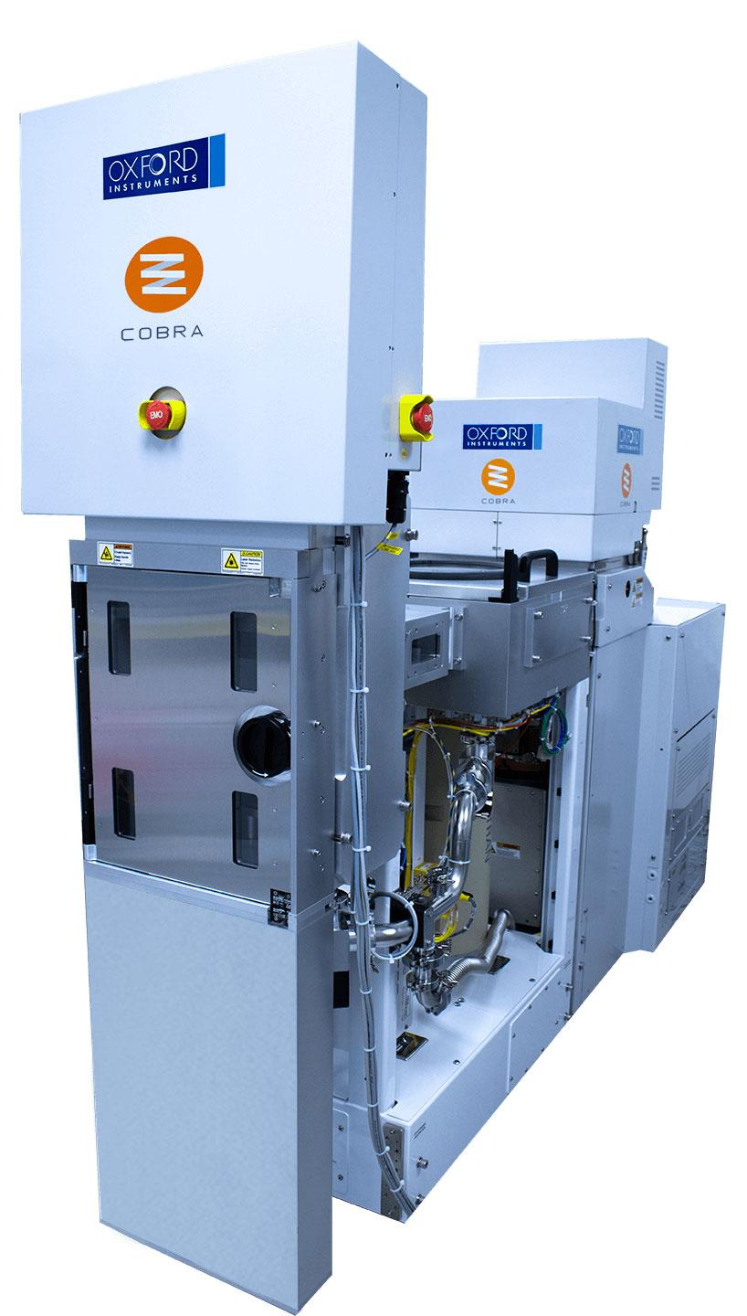
Chipmetrics’ CEO Mikko Utriainen is looking forward to testing Photonics Center’s potential as a research and development environment. The centre offers a range of equipment that is ideal for Chipmetrics’ needs, such as an ALD reactor, which can be used to test the functionality of products.

“It is also an enormous help to have the personnel of the University of Eastern Finland available for support at an hourly rate. Photonics Center’s equipment is demanding and requires highly skilled professionals. As a whole, the greatest benefit is certainly that all these resources are available in one place. No facilities of the same standard can be found in Eastern Finland; in fact, the only option in Finland would have been to transfer the company’s operations to Helsinki.”


Of the individual Photonics Center resources, the most important attraction factor for Chipmetrics was cleanrooms.

“The handling and development of our products must all be done in cleanrooms, as is typical in the semiconductor industry. That is why they are a necessity for a company like us.”

Measurement solution to increase efficiency in processes worth billions

Chipmetrics specialises in ALD technology. ALD stands for atomic layer deposition, which enablesmeans coating three-dimensional objects with thin film structures. ALD is a growing sector: according to Utriainen, the global market is approaching EUR 3 billion.

“ALD is used, for example, in semiconductor components, batteries and optical filters with 3D structures that are difficult to implement and coat. A smooth uniform thin film coating is very difficult, but it is even more difficult to measure whether the coating is really uniform smooth.”

Chipmetrics’ PillarHall solution is capable of very accurate measurement, enabling semiconductor manufacturers to enhance their own processes. Even small improvements can be valuable.

“The investments made by giant electronics companies are often in billions. A manufacturer of semiconductor equipment, which is best able to demonstrate its technical performance, can win a significantly sizeable deal in a big chip manufacturer’s factory investment. It is often important for our customer companies to be able to demonstrate to their own customers how well they can achieve a functioning process,” Utriainen explains.

Investors getting interested

Chipmetrics is a spinoff company that originated from a VTT research project. Utriainen was involved in the development of technology already at VTT. The company was established in 2019 and operational activities began at the end of 2020 when IPR rights were transferred to Chipmetrics.

The first full financial year was already good for the company: turnover was EUR 703,000 and profit was EUR 84,000. Chipmetrics just recently finished its start-upseed funding round, which netted EUR 340,000 for the company. The round was led by the North Karelia Growth Fund and four private investors. With the help of new funding, CEO Utriainen plans to develop the company’s product portfolio and expand the international sales network.

“ALD technology is complex, and it has been one of the key challenges for investors: sponsors naturally want to understand what they are participating in. We have now got investors involved in Finland, which also increases interest abroad.”

“It is our pleasure to welcome Chipmetrics to Photonics Center,” says Pauliina Pikkujämsä, Director of Business Services at Business Joensuu. “Photonics is one of the top industries in Joensuu, and Photonics Center is a direct investment in the operations of companies that manufacture or utilise photonics. ALD technology, the field of Chipmetrics, also has huge growth potential internationally. We’d like to have more such growth companies in the Joensuu region.”

Further information:

Pauliina Pikkujämsä

Business Services Director, Invest In and Relocation Services, pauliina.pikkujamsa@businessjoensuu.fi, +358 40,743 4362

Mikko Utriainen

Chipmetrics Oy, CEO, mikko.utriainen@chipmetrics.com, +358 40,753 7415


Business Joensuu

Business Joensuu Oy offers services for launching companies, growth and internationalisation, investing and setting up operations in an area, and space and event services of the Joensuu Science Park. Business Joensuu also produces growth and competitiveness programmes which create the best conditions for companies to operate in the Joensuu area.

Chipmetrics

Chipmetrics Oy is an ALD (Atomic Layer Deposition) technology company. Chipmetrics is the market leader in delivering productised nanotechnological high aspect ratio test structures to the semiconductor industry and emerging ALD applications. Chipmetrics’ headquarters are located in Joensuu. Further information: www.chipmetrics.com

Picture credits: Chipmetrics Oy

Thursday, September 15, 2022

ATLANT 3D Nanosystems Secures 15M USD Investments to Enable Atomic Layer Advanced Manufacturing for Electronics

Copenhagen September 12, 2022: ATLANT 3D Nanosystems (ATLANT 3D), today announced the closure of their capital raise of 15M USD. The round was led by UK venture capital firm West HillCapital and further supported by existing investors including a leading Japanese corporation. The funding is the largest joint Series A round in Denmark outside of life sciences and software.

The funding will be used to get one step closer to ATLANT 3D’s vision to create a network-centric smart advanced manufacturing infrastructure based on its proprietary technology and know-how and integrate it in the future with other advanced technologies. ATLANT 3D aims to develop a network of advanced manufacturing hubs – the A-hubs – across the globe to enable a radical innovation ecosystem for next-generation micro and nanoelectronics prototyping and manufacturing.

ATLANT 3D is the first and only company to crack the code for a radically new way of doing micro and nano processing. ATLANT 3D’sNanofabricator™ enables advanced manufacturing with AI solutions which allows direct patterning on complex surfaces, various substrate materials, plain wafers, and textures with existing structures or devices. ATLANT 3D technology has a unique configuration that allows atomically precise processing at micro and zero gravity. In general, it decreases the time and cost of processing from years and months to days, and gives unprecedented flexibility for material innovation, prototyping, and production of micro and nanodevices, replacing the previous cleanroom-based complex process flows.


“The existing process-intensive manufacturing method is a limiting factor in the future of electronics development. Due to its inflexibility, the current multi-step process is at the root of our current global supply chain crises, causing a shortage of electronics devices and bringing high barriers to innovation. “, says Dr. Maksym Plakhotnyuk, CEO and Founder of ATLANT 3D. “At ATLANT 3D, we have invented a unique technological platform that enables what was previously impossible. Imagine that new advanced materials, devices, and applications that you use today for your smart life or for the industry can be manufactured in-house, with flexibility, and sustainability in mind. The process can be fully digital, cost-effective, and provide a possibility for rapid innovation with atomic precision. The recently raised funding will enable us to continue the fast technology and product development and expand ATLANT 3D to the first international market.”

” We see a huge potential in ATLANT 3Ds' groundbreaking technology. We were impressed by the company’s grand vision and the way how ATLANT 3D technology is ready to disrupttodisrupt the conventional microfabrication approach” says Alan Richards, Partner, and Co-Founder of West Hill Capital.


ATLANT 3D is a Danish deep-tech company founded in 2018 developing a fundamentally different and innovative micro and nanofabrication platform technology that enables atomically precise advanced manufacturing of advanced materials and electronics with the vision to revolutionize electronics atom by atom. Since 2020ATLANT 3D secured a number of customers, leading global industrial companies and organizations, in space, semiconductor, and electronics industries.


Since 2014, West Hill Capital has arranged investment of $500 million into 40 early-stage high-growth companies in the UK and Denmark. In 2021, West Hill’sportfolio company Humio was acquired by USA Nasdaq-listed Crowdstrike Holdings for US$400 million, one of the largest Danish private company exits that year.b