Monday, August 31, 2020

High customer satisfaction with Picosun’s new service and support model


ESPOO, Finland, 31st August 2020 – Picosun Group’s growth strategy is based on strong expansion into industrial ALD markets. To support this strategy, special emphasis has been placed on strengthening the Group’s global service organization. The investment has paid itself back in the form of high level of customer satisfaction, despite the challenges caused by the global covid-19 pandemic especially in traveling and logistics.

“Due to the reinforced localization of our service and support units, our service engineers’ utilization level has been more than 85% in the past six months, and with the latest remote service and support tools we have gained advantage to manage our customers’ PICOSUN® ALD system commissionings online and in time. ALD tool maintenances, process development, spare parts and other critical deliveries are also provided locally with maximum safety precautions in place, to ensure customers continuous operation of their PICOSUN® ALD equipment,” states Mr. Timo Malinen, Customer Experience Director of Picosun Group.

During the last months, Picosun Group has hired and trained several new service engineers and sales and support personnel to provide local support at the Group’s US, Asian, and European locations. Remote diagnostics, control, and data logging features for remote troubleshooting and process optimization of customers’ PICOSUN® ALD tools are a routine approach in the Group’s ALD solution deliveries. Augmented and/or virtual reality solutions for even more efficient service operations and remote learning/e-training possibilities are also under development and will be introduced in all Picosun’s operations later on.

“Our principle of ‘AGILE ALD’ and our position as the technological forerunner in our field obligate us to provide the best possible services and solutions to our customers. As a globally operating company, pandemic risk scenarios are an integral part of our continuous risk planning. Against the backdrop of the current covid-19 outbreak, our service operations are continuously being adapted to mitigate potential impacts. Picosun Group follows a holistic management process that enables constant development of our customer service unit to ensure the best possible response even in an emergency situation,” continues Malinen.

For Picosun, the health of employees and customers is the highest priority. In order to closely monitor and manage the covid-19 situation, Picosun follows all the safety regulations provided by WHO, CDC, ECDC, and Finnish Institute for Health and Welfare, and provides the necessary information timely to all employees, customers, and other stakeholders.

Wednesday, August 26, 2020

Ereztech is excited to announce the 2020 BridgeForward™ Award

Ereztech is excited to announce the 2020 BridgeForward™ Award, a financial award recognizing gifted graduate students and recent post-doctoral graduates pursuing careers in organometallic chemistry or materials science. Eligible young scientists can submit their application for the chance to win one of five $1,500 awards. Learn more at ereztech.com/award


Nano-Engineered Surfaces Unlock New Material Capabilities

Forge Nano launches new tools to enable nano-tech research, using Atomic Layer Deposition


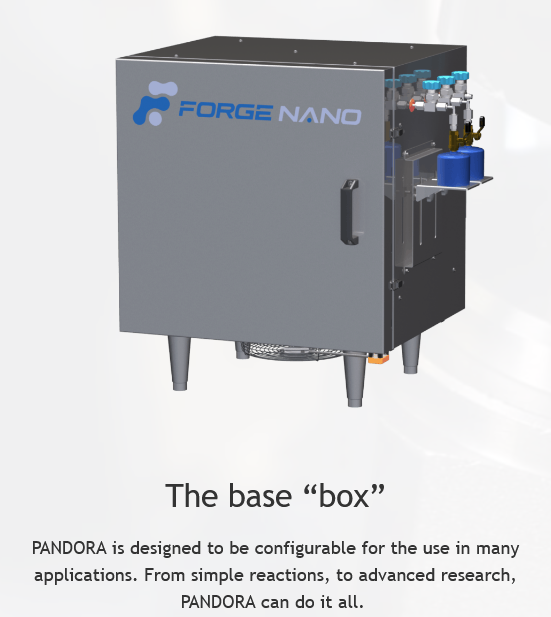
Putting recent investments to work, Forge Nano Inc. launches new tool to enable Particle Atomic Layer Deposition (PALD) development. Billed as a "PhD Thesis in a box," the PANDORA tool is an easy to use, configurable DESKTOP research tool unlike anything else. 


(Picture: forgenano.com)
 
PANDORA unlocks the potential of ATOMIC LEVEL surface engineering, in an impossibly compact form factor at an affordable price. PANDORA is built to exceed global and industrial standards, and comes with several configurations, including plasma. From energy storage materials to pharmaceutical research, PANDORA will help researchers develop revolutionary coatings across disciplines. More details are now available at: https://www.forgenano.com/pandora.

Forge Nano specializes in optimizing the way surfaces interact at an ATOMIC level. Using proprietary technology, Forge Nano can apply nano coatings onto the surface of virtually anything. Now Forge Nano puts that power into the hands of researchers everywhere with an easy to use, configurable DESKTOP unit that can lead to materials innovations anywhere in the world.

"By designing the way surfaces interact, we can optimize their performance in many ways. We are truly manufacturing with atoms. The applications for ALD and PALD are nearly endless. By adding partners like Sumitomo Corporation of Americas and ALIAD (Air Liquide Venture Capital), we can develop and introduce new technologies like PANDORA to the market more efficiently. By enabling innovation with a community of active users, and collaborating in Commercialization programs, we provide a clear path to scalability." Dr. Paul Lichty- CEO Forge Nano.

Monday, August 24, 2020

TechInsights ALD/ALE Process in Commercially Available Logic Devices

2018 saw the introduction of a new generation of logic products featuring finFET transistors headlined by Intel with their 10 nm generation microprocessor, followed by TSMC and Samsung towards the end of the year with their 7 nm node devices. 


This presentation on the Atomic Layer Deposition/Atomic Layer Etching (ALD/ALE) process examines some of the different structures we have seen during the evolution of these logic technologies, in particular the latest 7 nm and 10 nm devices. We also discuss several historical applications of ALD/ALE technology that have been observed through reverse engineering, and we highlight the importance of ALD/ALE process in advanced logic devices. In many cases, the technology could not have advanced without the implementation of ALD/ALE. 

Register here: LINK

Wednesday, August 5, 2020

Applied Materials launch Selective Tungsten CVD for their Endura(TM) platform

[Applied Materials Blog LINK] Tungsten has been widely used as a gapfill material in middle-of-line (MOL) contacts for its low resistivity and bulk fill characteristics. MOL contacts form the critical electrical link between the transistors and the interconnects. Hence, ensuring low resistivity contacts is crucial for overall device performance.

With continued scaling, however, contact dimensions have decreased to the point at which contact resistance is becoming a bottleneck in realizing optimum device performance. As the cross-sectional area of the contact shrinks, a growing proportion of the volume is occupied by metal liner/barrier and nucleation layers, leaving less volume for the conducting metal fill. In addition, multiple resistive interfaces in the plug contribute to higher contact resistance.

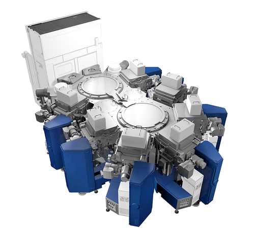
An Applied Materials Endura(TM) Platform equipped with seven Selective Tungsten CVD Volta(R) and 2 pre-clean 300 mm chambers. (Credit: Applied Materials)

The Applied Endura Volta Selective W CVD system offers an integrated materials solution that relieves these adverse effects with a breakthrough in 2D scaling. The system combines surface treatment chambers with selective tungsten deposition chambers. The selective deposition is enabled by both the unique process capabilities of the deposition chambers and the various surface treatments that use specialized chemistries to prepare the underlying metal and dielectrics of the contact to enable bottom-up, metal-on-metal deposition. The selective process eliminates both liner/barrier and nucleation layers to alleviate the bottleneck in device performance, and produces void- and seam-free gapfill.

Cross section of a leading edge Logic processor showing the Source/Drain contacts to the transistors and the metal interconnetcs (Credit: TechInsight, Applied Materials)

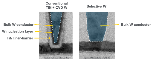
As all process steps are performed in an ultra-clean, continuous high-vacuum environment, the integrated materials solution ensures a pristine interface and defect-free contact fill. With the volume of conducting metal maximized, contact resistivity is substantially improved compared to conventional liner/barrier contact fabrication. This lower resistance facilitates higher device density and extends 2D scaling.

The selctive W CVD defect-free contact fill maximizes the volume of conducting metal (right), contact resistivity is substantially improved compared to conventional liner/barrier contact fabrication (left). (Credit: Applied Materials)

Monday, August 3, 2020

BDEAS - a versaitile ALD precursor for high quality dilectric films in leading edge semiconductor applications

One of the most important reasons why Silicon (Si), in place of Germanium (Ge), was propelled to the front of the class in the semiconductor industry from the very beginning, is the fact that Si forms a very stable oxide-semiconductor interface with SiO2. A high-quality oxide interface is a key to making field-effect transistors (MOSFETs). Germanium oxide is water-soluble which rendered it useless for MOSFET fabrication in the early days (now the industry is advanced enough to possibly solve that).

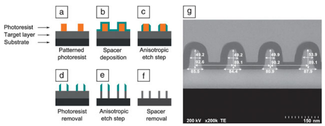
Thermal oxidation of Si at temperatures > 800 °C yields SiO2. To avoid such high temperatures and long processing times and tune the material properties, (wet) chemical oxidation, (plasma-enhanced) chemical vapor deposition or sputtering and electron beam evaporation are also preferred methods to grow SiO2. The advantages of precise thickness control, optimal large-area uniformity, and the conformality over demanding substrate topologies of atomic layer deposition (ALD) based SiO2 films, all led to an expansion of target applications such as; spacer based self-aligned double/quadruple patterning (SADP or SAQP) in fabricating DRAM and logic chips (Link), interface engineering between Si and high-k materials (Link), moisture barrier or protective or insulator coatings (Link), nanolaminate structures with tailored optical and electronic properties (Link) and double layer surface passivation in Si photovoltaics (Link), etc. to name but a few.


Link for the image

Bis(diethylamino)silane (BDEAS) [SiH2[N(CH2CH3)2]2, also known as SAM-24[MP1] , is one of the most preferred Si precursors for ALD of SiO2 and other Si-containing films. It’s an air-sensitive, moisture-sensitive, flammable, colorless, and odorless liquid precursor (boiling point 70 °C (30mm), density 0.804), which exhibits a high vapor pressure, i.e. ~100 Torr at 100 °C.

The research group of Prof. W. M. M. Kessels, Department of Applied Physics, Eindhoven University of Technology, has reported that BDEAS is suited for low-temperature synthesis of high-quality SiO2 by ALD with the SiO2 properties being relatively insensitive to the substrate temperature for the temperature range of 100 – 300 °C; for temperatures reaching 400 °C thermal stability issues of the precursor and its ligands start to play a role. The process is also relatively fast as it combines a high growth-per-cycle (0.8 – 1.7 Å/cycle) with relatively short dosing and purge times. The ALD SiO2 processes with BDEAS precursors are therefore of interest for high-volume manufacturing applications, for instance, using ALD batch processes or inline (plasma) ALD equipment.

Link for the image

Strem Chemicals, Inc., a high purity specialty chemicals manufacturer and supplier, headquartered in Newburyport, Massachusetts, USA, boasts a vast variety of ALD/CVD precursors, including BDEAS for depositing Si-based films in different applications.

Since 1964, Strem Chemicals, Inc. has been serving its clients from academic, industrial, and government research and development laboratories as well as commercial scale businesses in the pharmaceutical, microelectronic, and chemical/petrochemical industries. Strem also provides custom synthesis (including high-pressure synthesis) and current good manufacturing practice (cGMP) services. With ISO 9001 certification for the Quality Management System (QMS) standard and documentation, Strem products are high purity materials, typically 99%, with some at 99.9999% metals purity. Strem utilizes a comprehensive range of analytical techniques tailored to each product to ensure quality because  researchers typically rely on the supplier's quality procedures and documentation, which if poorly conducted[MP1]  may kill a great research idea. All of Strem's catalogs, since inception, have listed “Color and Form” for every product as primary indicators of quality.


 [MP1]SAM-24 may be an Air liquide trademark.

----------

Promotional blog written and researched by Abhishekkumar Thakur and Jonas Sundqvist, BALD Engineering AB