Wednesday, June 28, 2017

Formation of BiFeO3 from a Binary Oxide Superlattice Grown by ALD

Drexel University has been developing Bi-Fe-O ferroelecttrics (and others) for many years and here they report on ALD of polycrystalline BiFeO3 thin films on SiO2/Si(001) by ALD using  ferrocene, triphenyl-bismuth, and ozone. Due to its ferroelectric properties BiFeO3 is intersting for future non-volatile memory (FeFETs and FRAM). The ALD of Bi-Fe-O thin films were carried out in a Picosun R200 Advanced Reactor (Supporting Information, for all the process details).


However, iron is not likely to be used in a standard 300mm CMOS fab today, neither in front nor in backend of line - it´s just diffusing to fast to places it is not wanted. But that said, a stand alone memory technology in a dedicated fab may find ways to handle that. The other contender for novel highly scaled ferroelectric metal oxides is the HfO2 based systems researched by NaMLab, Fraunhofer and GloFo in Dresden Germany. Those systems looks much more promising since they are already shuffling leading edge 300 mm wafers since a while now and HfO2 has been in HVM since 2004 (Samsung 90 nm DRAM, HfAlOx MIS stack). The HfO2 ferroelectric R&D has been going on for more than 10 years actually. This just show s how long time materials and device development takes in the semiconductor industry


Formation of BiFeO3 from a Binary Oxide Superlattice Grown by Atomic Layer Deposition


ChemPhysChemEarly View, Version of Record online: 20 JUN 2017
DOI: 10.1002/cphc.201700407

Abstract: By growing alternating layers of Fe2O3 and Bi2O3, we employ a superlattice approach and demonstrate an efficient control of the cation stoichiometry. The superlattice decay and the resulting formation of polycrystalline BiFeO3 films are studied by in situ X-ray diffraction, in situ X-ray photoelectron spectroscopy, and transmission electron microscopy. No intermediate ternary phases are formed and BiFeO3 crystallization is initiated in the Bi2O3 layers at 450 °C following the diffusion-driven intermixing of the cations. Our study of the BiFeO3 formation provides an insight into the complex interplay between microstructural evolution, grain growth, and bismuth oxide evaporation, with implications for optimization of ferroelectric properties.

Tuesday, June 27, 2017

The Dubbo Project - The High-k mine in Dubbo, NSW Australia

Unknowingly I´ve been camping and going through in Dubbo two times, literally our tent was on top of a high-k mine without me knowing it! They have got it all there Down Under: zirconium, hafnium, niobium, tantalum and all of the rare earths. Just take a moment to check out the videos below and stay tuned for more on the Dubbo project.


The Dubbo Project (DP) is a new and strategically significant source of high demand critical metals, which are independent of traditional supply sources. The Dubbo resource is a long life polymetallic ore body that is readily processed and separated into valuable products including zirconium, hafnium, niobium and rare earths.


A large scale Demonstration Pilot Plant at ANSTO in Sydney has been operating since 2008 to provide robust qualification and optimisation of the DZP process and the necessary information for scale up to a full scale operating plant. The plant has proven the process flowsheet from a chemical and engineering sense as well as providing capital and operating costs for scale-up.
 

Over 100 tonnes of ore has been processed in the Demonstration Pilot Plant to produce zirconium, hafnium, niobium and rare earth products.

At a processing rate of 1 m tpa of ore for the full scale plant, annual revenue for the four product groups ranges from US$430m - US$470m pa with an EBITDA of $235m - $275m pa.

Picosun’s ALD solutions enable non-volatile memories (ReRAM)

As previously reported here (LINK) New prospects for universal memory from MIPT Russia using Picosun ALD: ESPOO, Finland, 27 June, 2017 – Picosun Oy, leading supplier of high quality Atomic Layer Deposition (ALD) thin film coating solutions, reports of breakthrough results achieved with its ALD technology in development of novel high-speed memories. These memories are required in state-of-the-art data storage applications, where a combination of very large capacity and extremely fast operating speed is needed. The results have been obtained at Picosun’s long-term customer Moscow Institute of Physics and Technology (MIPT), Russia.


Experimental cluster, including a Picosun ALD reactor, for growing and studying thin films in a vacuum at the Center of Shared Research Facilities, MIPT

ReRAM (Resistance Switching Random Access Memory) is a new, non-volatile memory type which has the attributes to become the much sought-after universal memory to replace and outperform the current technologies, and to solve the ever-growing demand for more and more efficient data storage systems. ReRAM is fast, small, structurally simple, it has high capacity and it operates at low voltages. These features help to decrease the device size, power consumption, and response time, allowing yet smoother-operating electronic end products. Smaller operating voltage enables ReRAM integration also to low-power devices such as portable, wearable, and mobile electronics, remote sensing and IoT (Internet of Things) applications, the number of which is growing explosively at the moment.

Monday, June 26, 2017

Umicore inaugurates new production facility in Germany

Umicore reports: Umicore’s business unit Precious Metals Chemistry inaugurated today its innovative production unit for advanced metal organic precursor technologies used in the semiconductor and LED markets, respectively TMGa (Trimethylgallium) and TEGa (Triethylgallium). The event was attended by European and overseas customers as well as local and regional politicians. The guest of honour was Dr. Barbara Hendricks, Germanys Federal Minister for the Environment, Nature Conservation, Building and Nuclear Safety.
Umicore TMGa (Trimethylgallium) and TEGa (Triethylgallium) facility in Hanau, Germany (photos supplied by Umicore).
Umicore’s TMGa manufacturing process is innovative and unique. It offers a more sustainable and ecological production method by minimizing hazardous side streams and material losses and optimizing yield to nearly 100%. This makes it superior to all existing manufacturing methods in the industry.

Umicore TMGa (Trimethylgallium) and TEGa (Triethylgallium) facility in Hanau, Germany (photos supplied by Umicore).
Dr Lothar Mussmann, Vice-President of Umicore Precious Metals Chemistry said “I am proud that this patented innovation has now become a world-class and industrial scale manufacturing plant. It will provide benefits for our customers and the environment and underlines Umicore’s position as a pioneer in sustainable technologies.”
Umicore TMGa (Trimethylgallium) and TEGa (Triethylgallium) facility in Hanau, Germany (photos supplied by Umicore). 

Umicore Precious Metals Chemistry is the only European manufacturer of TMGa and TEGa and supplies customers across the world from its Hanau manufacturing base. Umicore Precious Metals Chemistry helps to reduce cost of ownership through its innovative approach to process chemistry and its collaborative approach with customers and end users.

TECHCET Advanced Dielectric Precursors CMR™ – Just Released!

The Dielectric Precursors Critical Materials Report (CMR) provide detailed market, supply chain and technology trend information required for anyone developing strategy for their business, be it a materials supplier or semiconductor chip manufacturer. Precursor types include, gapfill, ILD, low K, and multi-patterning. The report is written by Jonas Sundqvist and edited by Ed Korczynski.


Full table of contents : LINK

TECHCET Reports can be Included with CMC Membership – Click Here for Info!


Friday, June 23, 2017

Yole Développment is releaseing the Emerging Non-Volatile Memory 2017 June 28

Yole Développment: The key emerging non-volatile technologies like phase-change memory (PCM), magnetoresistive random access memory (MRAM) and resistive random access memory (RRAM) have long development histories. Yet, their adoption remains restricted to niche markets due to various factors. Available products have limited density, and the introduction of high density products by emerging NVM pioneers has been delayed. There are manufacturing challenges due to the introduction of new materials and process steps. Meanwhile, mainstream memory technologies are continuously improving in terms of density and cost. Finally, there has been an absence of a killer application that would challenge dynamic random access memory (DRAM) and NAND flash memory. [read further, LINK] - Thanks to Terry Francis for sharing this one!

 Time to market for differen memory technologies  (Yole Développment, LINK)

Unfortunately, Yole does not mention here the developments in Ferroelectric hafnium oxide based FeFET and FRAM (by NaMLab, Fraunhofer and Globalfoundries). There has been quite some progress over a 10 years development (originally imitated and discovered by Qimonda R.I.P.) so far and most recent approach by Imec integrating Ferro FETs in a bit scalable 3D-NAND style architecture. The main advantage of this technology is that in the case of a logic embedded memory cell and a stand alone 3D-NAND style version standard equipment and process flows can be used in HVM. In addition, according to Imec memory Guru Jan van Houdt, "It [FeFETs] has particularly interesting characteristics for future storage-class memory, which will help overcome the current bottleneck caused by the differences in speed between fast processors and slower mass memory"

The last couple of years there is an increased IP filing in hafnium oxide and related technologies and precursors and especially for ferroelectric memory. It was also apparent by studying the last VLSI program that there are man more mature activities in this technology and if I remember correctly there was 6-8 presentations on this topic. Possibly the report itself gives some insights also to the status of ferroelectric NVM technologies.

 
Imec is confident that their FeFET concept has all the required characteristics for both stand-alone and embedded memories, from non-volatile DRAM to Flash-like memories. (2017 Symposia on VLSI Technology and Circuits, Kyoto Japan June 7, 2017, source www.imec.be) 
 

Thursday, June 22, 2017

Leading edge ALD is a technology enabler for trailing edge

According to a recent article in Semiconductor Engineering on the reworking of established nodes (May 24th, 2017 - By: Ed Sperling, LINK) the benefits of device scaling don’t apply equally to all markets. However, the process technology does. A good example of this is, according to my opinion, is ALD high-k (Al2O2, ZrO2, HfO2, Ta2O5 etc.) MIM Caps that have multiple HVM applications in 200mm fabs around the world. As well as ALD liners and etch stops in MEMS and LED production.

According to Ed Sperling, that " .. is why the foundries, equipment makers and packaging houses have introduced a menu of possible options at established nodes, including new materials as well as new process options, including low-power, ultra-low power, high-performance and low-cost options at the same nodes."


Interestingly this also applies to ALD for high volume manufacturing and in an interview with ASM Peter Zagvijn, senior technical product manager a message was given:

“By using thin films on 200mm you can get higher function but still have low cost. This is a technology enabler. It will be important for high-voltage electronics and electric cars because it allows you to extend the platform maintainability and the lifetime of the equipment by transferring what happens at the leading edge to the lagging edge. Using ALD technology, there are more than 50 films available for diffusion on one platform.”

In addition, Zagvijn said that ALD technology and capability will be important in wafer-level packaging.

Tuesday, June 20, 2017

Light, Superelastic, Electrically Conductive, and Flame-Retardant Graphene / ALD Ceramic Metamaterial

Researcher from Lanzhou University (China) and Purdue University (USA) has developed a new ceramic/graphene wonder metamaterial (GCM) with microstructure-derived superelasticity and structural robustness is achieved by designing hierarchical honeycomb microstructures

The GCM is composited by two brittle constituents (graphene and ceramic) assembled in multi-nanolayer cellular walls. The GCM demonstrates a sequence of multifunctional properties simultaneously that have not been reported for ceramics and ceramics–matrix–composite structures, such as: 
  • flyweight density
  • 80% reversible compressibility
  • high fatigue resistance
  • high electrical conductivity
  • excellent thermal-insulation/flame-retardant performance simultaneously. 


All details can be find in the Advanced Materials publication below. According to the suppoirting information the Al2O3 ceramic depositions were performed in an Utratech Fiji F200 ALD system (pictured above) at 250 C using trimethylaluminum (TMA) and H2O as the aluminum and oxygen source, respectively.


Flyweight, Superelastic, Electrically Conductive, and Flame-Retardant 3D Multi-Nanolayer Graphene/Ceramic Metamaterial
Qiangqiang Zhang et al
Adv. Mater., DOI: 10.1002/adma.201605506

Beneq in 2016 – A Successful Strategic Transformation

Beneq’s financial figures from 2016 show growth, encouraging signs of transformation, and positive development in industrial ALD solutions. Beneq corporation turnover grew to 22,2 million euros in 2016. And Beneq is a truly global company: 98% of the company turnover came from outside Finland.

The year 2016 was a transformation year for Beneq in many ways. In Thin Film Solutions, there was a shift from traditional ALD research equipment towards large-scale industrial ALD equipment and thin film services – a trend which has continued during 2017. The equipment business order flow in the first quarter of 2017 was 70% higher than during Q1/2016 with several new industrial ALD customers and repeat orders from customers who are expanding ALD-based industrial production.
For the Thin Film Solutions business unit, major development areas are industrial ALD equipment and continuous large-area ALD processes based on Beneq’s pioneering Spatial ALD technology, which allows fast low-cost processing of materials in industries that require extremely precise coatings and high capacity, such as OLED and flexible electronics markets.

Monday, June 19, 2017

TECHCET ALD/CVD High-k & Metal Precursors CMR™ – Just Released!

The TECHCET ALD/CVD High-k & Metal Precursors Critical Materials Report provides information on the applications, IP-filing and markets associated with front end and back end of line precursors used to produce high-k dielectrics, metals, meatl oxides and nitrides by atomic layer deposition (ALD) and chemical vapor depsotion (CVD) metal oxides and nitrides. The report is written by Jonas Sundqvist and edited by Lita Shon-Roy.


Full table of contents : LINK

TECHCET Reports can be Included with CMC Membership – Click Here for Info!


Sunday, June 18, 2017

New prospects for universal memory from MIPT Russia using Picosun ALD

MIPT Reports: Researchers from MIPT’s Center of Shared Research Facilities have found a way to control oxygen concentration in tantalum oxide films produced by atomic layer deposition. These thin films could be the basis for creating new forms of nonvolatile memory.

The MIPT non-volatile ReRAM memory cell is based on ALD deposited tantalum oxide using tantalum ethoxide and water.

“The hardest part in depositing oxygen-deficient films was finding the right reactants that would make it possible to both eliminate the ligands contained in the metallic precursor and control oxygen content in the resulting coating,” says Andrey Markeev, who holds a PhD in physics and mathematics and is a leading researcher at MIPT. “We achieved this by using a tantalum precursor, which by itself contains oxygen, and a reactant in the form of plasma-activated hydrogen.”

Experimental cluster, including a Picosun ALD reactor, for growing and studying thin films in a vacuum at the Center of Shared Research Facilities, MIPT

ALD/ALE2017 Mobile App

Soon it is time for the next major event for the ALD and ALE community - ALD/ALE2017 in Denver Colorado. You can download the Mobile App for Android and Iphone here : LINK.


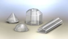
Atomic Layer Deposition for Coating of Complex 3D Optics by LASEROPTIK

Here is a great overview on ALD for coating complex 3D compnents for optics from LASEROPTIK, Germany (LINK).

Laseroptik offers ALD coatings ranging from UV to IR.

Atomic Layer Deposition for Coating of Complex 3D Optics - From theory to practice 

Abstract: Atomic Layer Deposition (ALD) is a chemical vapor coating technique that has recently been adapted for precision laser optics to perform highly conformal multilayer coatings on complex 3D substrates like hemispheres, axicons or multi-sided prisms. In our brief report, we explain some ALD fundamentals and describe the way from idea and single-layer films to simple AR (anti-reflection) coatings and even more ambitious designs, like non-polarizing beam splitters, performed on complex optical substrates.

The article contains a new nice graphical representation of CVD vs. ALD process description that I have not seen before - reminds me of winter vs an April typ of weather changing all thee time between winter and summer, rain, snow and sunshine.


LASEROPTIK is a German manufacturer of high power laser optics and coatings from VUV to IR, using PVD methods like e-beam evaporation, ion assisted deposition, magnetron sputtering, ion beam sputtering and recently the chemical vapor method of atomic layer deposition. LASEROPTIK runs more than thirty coating machines  and processes about 150,000 optics per year, from needle head size to laser mirrors of up to two meters in length. The company was founded in 1984 by Dr. Johannes Ebert as a spin-off from Hanover University. Main customers are laser manufacturers from industry, medicine and scientific research. 

Saturday, June 17, 2017

Forge Nano & NREL in Exclusive Licensing Agreement for battery materials

Agreement enables Forge Nano to fundamentally enhance lithium-ion battery safety, durability, and lifetime

The U.S. Department of Energy’s National Renewable Energy Laboratory (NREL) has entered into an exclusive license agreement with Forge Nano to commercialize NREL’s patented battery materials and systems capable of operating safely in high-stress environments. A particular feature of the technology is the encapsulation of materials with solid electrolyte coatings that can be designed to meet the increasingly demanding needs of any battery application. Read more...


Friday, June 16, 2017

Day 4 (Wednesday) EuroCVD-Baltic ALD 2017 in Linköping, Sweden

Here is a collection of tweets from Day 4 (Wednesday) EuroCVD-Baltic ALD 2017 in Linköping; Sweden.

Keep seeing these FABulous bags everywhere, must be the it-item of the season! (FAB Support sweden, Twitter)

ALD Lab Saxony, Cool Silicon e.v. participation and Exhibition at EuroCVD-Baltic ALD 2017 in Linköping, Sweden


ALD Lab Saxony  participated in the EuroCVD-Baltic ALD 2017 Conference in Linköping, Sweden 11th to 14th of June 2017. The ALD Lab Saxony members (IHM, TU Dresden), Fraunhofer ENAS and Fraunhofer IKTS) gave presentations and posters in the following fields:
  • Precursors (design, synthesis and delivery)
  • Process Equipment (reactors)
  • Nanomaterials (particles, 2D-materials, nano structures)
  • In-situ monitoring (QCM, Ellipsometry, IR, syncrotron)
  • Nitrides (semiconductors, conductors, hard coatings)
  • Carbides (hard coatings, semiconductors)
  • Elemental films (metals, amorphous carbon)
  • Emerging materials (hybrid MLD/ALD, sulfides)
ALD Lab Saxony also took active part in the exhibition with a joint table together with Colnatec the QCM Sensor company from Arizona USA and PillarHall(TM) team from VTT Finland presenting silicon wafers and chips that enable easy analysis of thin film conformality using well-defined, record-demanding microscopic 3-D structures.


Christoph Hossbach, now at Picosun Germany (a member of ALD Lab Saxony) taking the grand stage presenting on Area Selective ALD (Photo credit: Professor Henrik Pedersen, Twitter)


Marcel Junige (TU Dresden) presenting a poster on ALD Gold precursor candidates (photo credit: Marcel Junige)


Joint exhibition table with Colnatec USA (Wendy Jameson) and VTT Finland (Photo credit: Colin Georgi)


Fraunhofer IKTS (Jonas Sundqvist) presented via video link the latest developments on Hard coatings by CVD and ALD on WC Powder (Photo Credit Jonas Sundqvist)