Showing posts with label optical coatings. Show all posts

Monday, May 18, 2020

High-index-contrast gratings for III-nitride vertical-cavity surface-emitting laser diodes

Semiconductor Today reports that researchers based in Taiwan and Sweden claim the first demonstration of high-index-contrast grating (HCG) as the top mirror for III-nitride (III-N) vertical-cavity surface-emitting laser (VCSEL) diodes [Tsu-Chi Chang et al, ACS Photonics, published online 26 February 2020]. The team from National Chiao Tung University and Chalmers University of Technology hope that the development will lead to “substantial thickness reduction, polarization-pinning, and setting of the resonance wavelength by the grating parameters”.

Please follow the link below to find out where ALD was used ;-)

Article: High-index-contrast gratings for III-nitride vertical-cavity surface-emitting laser diodes (LINK)

Picture from graphical abstract, ACS Photonics 2020, 7, 4, 861-866 Publication Date:February 26, 2020
https://doi.org/10.1021/acsphotonics.9b01636

Monday, April 20, 2020

Anti-reflective optical coatings by ALD

[BENEQ] The challenge when coating 3D optics is to deposit the coating with high uniformity over an arbitrary topology in a simple manner. Commonly used techniques so called line-of-sight methods cause a non-uniform thickness distribution and shadowing effects. To alleviate this problem extensive mechanical work and process optimization is required, and this may still not lead to a sufficiently homogeneous film deposition. ALD overcomes those constraints and has proven its suitability for high precision pinhole free films, where the challenge is not only to achieve uniformity over a large scale, but to coat conformally over high aspect ratio structures of arbitrary shapes.

More information: Anti-reflective optical coatings (LINK)


Monday, March 30, 2020

Photonics for optical data transmission with Picosun’s Erbium ALD solutions

ESPOO, Finland, 30th March 2020 – Picosun Group reports excellent results in development of state-of-the-art photonics with its ALD (Atomic Layer Deposition) equipment and solutions.


Photonic devices such as waveguide amplifiers and lasers are central components in optical data transmission, a key technology realizing our modern, connected, information-driven society.

Silicon-integrated photonics take the technology one step further, enabling a whole new generation of microelectronics where optical solutions overcome some of the key challenges of conventional technologies.

Erbium-doped waveguide amplifiers and lasers are the most potential candidates for signal generation and amplification for telecommunication wavelengths. To reach the maximum performance of these devices, the amount and spatial distribution of dopant erbium atoms in the host material must be carefully optimized and controlled. This is where ALD shows its unique strength and beauty.

At Aalto University, Finland, Picosun’s customer Prof. Zhipei Sun’s group at the Finnish national infrastructure Micronova, and his international collaborators, have now used Picosun’s ALD technology to manufacture erbium-based silicon-integrated waveguide amplifiers with world-record performance(*).

“Silicon-integrated photonics, already employed by the leading companies in the field, are the future of microelectronics. We are very pleased of the performance of our PICOSUN® ALD equipment and the excellent quality of the Er:Al2O3 waveguide amplifiers manufactured with it. Customer support and consultancy from Picosun have always been there when we need it. ALD process is CMOS-compatible, further facilitating the integration of our waveguides into commercial chip production,” states Dr. John Rönn, the leading author of the results, from the Department of Electronics and Nanoengineering at Aalto University.

”ALD has been enabling disruptive future technologies since its invention. Picosun is happy to work with the leading experts in the field, such as our esteemed customers at the Aalto University. Our ALD solutions provide them the means to realize their groundbreaking work to develop yet more advanced communications and data transmission technologies for more connected, open, and integrated global society,” continues Mr. Edwin Wu, CEO of Picosun Asia Pte. Ltd

(*) The results were published in the journals ACS Photonics 3, 2040-2048 (2016) and Nature Communications 10, 432 (2019).

Monday, June 10, 2019

UV Broadband Antireflection Coating Using Al2O3, HfO2 and SiO2 Multilayer by ALD

Researchers at Shanghai Institute of Technical Physics of The Chinese Academy of Sciences have studied UV broadband antireflection (AR) films prepared by ALD. The study reports results in the 250~390 nm spectral range. They showed that a higher transmittance was acquired when HfO2-Al2O3 nano-laminates replaced the sinngle HfO2 layer in the AR coating. The results was presented at the recent Optical Interference Coatings 2019 conference in Santa Ana Pueblo, New Mexico United States (2–7 June 2019).

Trancmitance of ALD AR coating. (Figure capture from Google)

Source: OSA Publishing, Optical Interference Coatings 2019 "UV Broadband Antireflection Coating Using Al2O3, HfO2 and SiO2 Multilayer by Atomic Layer Deposition" LINK

Tuesday, February 5, 2019

Ultra-high on-chip optical gain in ALD erbium-based hybrid slot waveguides

Reliable on-chip optical amplifiers and light sources can enable integration of active functionalities on silicon based platforms.

Previously lasers integrated on silicon has been demonstrated with semiconductors by using methods such as wafer bonding or molecular beam epitaxy (MBE). These methods are however not that cost-effective in high volume manufacturing.

Now rearchers at Aalto University and Université Paris-Sud has now managed to significantly improve within chip data transmission using ALD Er:Al2O3 - a CMOS-compatible and scalable atomic-layer deposition process.

"The unique layer-by-layer nature of atomic-layer deposition enables atomic scale engineering of the gain layer properties and straightforward integration with silicon integrated waveguides. We demonstrate up to 20.1 ± 7.31 dB/cm and at least 52.4 ± 13.8 dB/cm net modal and material gain per unit length, respectively, the highest performance achieved from erbium-based planar waveguides integrated on silicon. Our results show significant advances towards efficient on-chip amplification, opening a route to large-scale integration of various active functionalities on silicon." [Nature Communications 2019, LINK]


Sunday, October 28, 2018

Fabrication of buried nanostructures with flat surface by ALD


Fabrication of buried nanostructures by atomic layer deposition (Open Access)

Rizwan Ali, Muhammad Rizwan Saleem, Matthieu Roussey, Jari Turunen & Seppo Honkanen Scientific Reportsvolume 8, Article number: 15098 (2018) 

We present a method for fabricating buried nanostructures by growing a dielectric cover layer on a corrugated surface profile by atomic layer deposition of TiO2. Selecting appropriate process parameters, the conformal growth of TiO2 results in a smooth, nearly flat-top surface of the structure. Such a hard surface can be easily cleaned without damage, making the nanostructure reusable after contamination. The technique has wide applicability in resonance-domain diffractive optics and in realization of quasi-planar metamaterials. We discuss design issues of such optical elements and demonstrate the method by fabricating narrow-band spectral filters based on the guided-mode resonance effect. These elements have strong potential for, e.g., sensing applications in harsh conditions.


Fabrication process of ALD-TiO2 buried guided mode resonance filters (GMRFs). Shared under Creative Commons Attribution 4.0 International License From: Fabrication of buried nanostructures by atomic layer deposition


Wednesday, March 14, 2018

RMD Dynasil employ CdTe ALD process for passivating HgCdTe IR sensors

Dynasil’s Radiation Monitoring Devices (RMD) is a world-renowned expert in the scintillation, photodetection, and radiation detection industries. At the recent Dynasil Corporation of America Annual Stockholder Meeting and Investor Presentation Conference Call it was reveiled that they have commericiallized an ALD process for passivating HgCdTe sensors with semiconductor-grade CdTe layer. The ALD coating is conformal, continuous and pinhole-free. Such low temperature CdTe ALD films have been previously published by Bengi Hanyaloglu et al (LINK).

Applications for these sensors are for:
  • Space IR telescopes
  • Tactical night vision googles and binoculars etc.
Peter Sulick - Chairman, President & CEO has this to say about the application (Seeking Alpha call transcript LINK)

"Another exciting area for research that is going on at RMD is its activation of the mercaptal infrared arrays, third-generation infrared arrays, and as people in the optic suite are well aware, this mercaptal infrared arrays require stabilization on the surfaces because of the semiconductor bonds being open at the surfaces. And one of the ways to do that is through activation layer of mercaptal films, and RMD has developed a proprietary technology using atomic layer deposition to deposit this mercaptal films. And the important advantage that our technology brings is that these are controllable films, which can be deposited at much lower temperatures than currently thought, and that can have a big impact in the yield and in the utility of these infrared sensors. So we are excited about where this area is going."


RMD has developed an ALD process for passivating HgCdTe sensors with semiconductor-grade CdTe layer. The ALD coating is conformal, continuous and pinhole-free. (Dynasil 2018 Annual Meeting Management Presentation LINK


Sunday, June 18, 2017

Atomic Layer Deposition for Coating of Complex 3D Optics by LASEROPTIK

Here is a great overview on ALD for coating complex 3D compnents for optics from LASEROPTIK, Germany (LINK).

Laseroptik offers ALD coatings ranging from UV to IR.

Atomic Layer Deposition for Coating of Complex 3D Optics - From theory to practice 

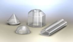
Abstract: Atomic Layer Deposition (ALD) is a chemical vapor coating technique that has recently been adapted for precision laser optics to perform highly conformal multilayer coatings on complex 3D substrates like hemispheres, axicons or multi-sided prisms. In our brief report, we explain some ALD fundamentals and describe the way from idea and single-layer films to simple AR (anti-reflection) coatings and even more ambitious designs, like non-polarizing beam splitters, performed on complex optical substrates.

The article contains a new nice graphical representation of CVD vs. ALD process description that I have not seen before - reminds me of winter vs an April typ of weather changing all thee time between winter and summer, rain, snow and sunshine.


LASEROPTIK is a German manufacturer of high power laser optics and coatings from VUV to IR, using PVD methods like e-beam evaporation, ion assisted deposition, magnetron sputtering, ion beam sputtering and recently the chemical vapor method of atomic layer deposition. LASEROPTIK runs more than thirty coating machines  and processes about 150,000 optics per year, from needle head size to laser mirrors of up to two meters in length. The company was founded in 1984 by Dr. Johannes Ebert as a spin-off from Hanover University. Main customers are laser manufacturers from industry, medicine and scientific research. 

Monday, June 15, 2015

University of Cincinnati and Industry Partners Develop Low-Cost Tunable Window Tintings

As reported by University of Cincinnati - Technology developed by the University of Cincinnati and industry partners can do something that neither blinds nor existing smart windows can do. This patent-pending research, supported by the National Science Foundation, will lead to low-cost window tintings which dynamically adapt for brightness, color temperatures and opacity (to provide for privacy while allowing light in). 


Top view and side-view diagrams of the device construction.

Technology developed by the University of Cincinnati and industry partners can do something that neither blinds nor existing smart windows can do. This patent-pending research, supported by the National Science Foundation, will lead to low-cost window tintings which dynamically adapt for brightness, color temperatures and opacity (to provide for privacy while allowing light in). 


Full story here : http://www.uc.edu/news/NR.aspx?id=21741

Thursday, August 7, 2014

Reflectionless Transmission through Dielectrics by ALD

As reported by The Times of India: Three-year-long targeted research by Tata Institute of Fundamental Research team led by Professor Achanta Venu Gopal with design and simulation input from a senior optics faculty at University of Hyderabad, Professor S Dutta Gupta, has led to the experimental confirmation of a US patent (no: US 7,894,137 B2).
 
The patent is jointly owned by UoH and Oklahoma State University (OSU), with inventors Professor S Dutta Gupta (UoH) and Prof. Girish Agarwal (OSU) and deals with complete transparency of a graded index dielectric film based on the concept of reflectionless potentials. The notion of reflectionless potentials was proposed by Kay and Moses (I. Kay and H. E. Moses, "Reflectionless transmission through dielectrics and scattering potentials," J. Appl.Phys. 27(12), 1503-1508 (1956)). It was extensively used in inverse scattering and high energy physics theory. Incidentally there were very few research efforts in optics.
 
I. Kay and H. E. Moses, "Reflectionless transmission through dielectrics and scattering potentials," J. Appl.Phys. 27(12), 1503-1508 (1956)).
 
The realization of the optical reflectionless potential opens up new directions for a totally new design methodology for omnidirectional broadband optical coatings to enhance the throughput of any optical device. Note that standard antireflection coatings mostly makes use of quarter wavelength plates, and thus cannot be broadband and omnidirectional. The realisation of optical reflectionless potentials was a real experimental challenge in the context of choice of materials and finding the optimal technique. The graded reflectionless profile was achieved with Titanium and Aluminium oxide nano layers since they have high and low refractive indices, respectively, and a proper combination can lead to an effective medium with intermediate desired refractive index.

"We had to explore different layer deposition techniques since nanometer thick layers needed for the profile have different optical properties depending on the technique. We had to use techniques ranging from atomic layer deposition, electron beam evaporation to sputtering. We are still in the process of refining the growth process", says Prof. Gopal.
 
There are other fundamentally interesting properties like superluminal group velocities, pulse narrowing etc., which are being probed. Note that superluminal group velocities do not violate Einstein's principles, since the peaks of the emerging and incident pulses are not causally related.