Wednesday, December 18, 2019

2020 CMC Conference New Session on Advanced Packaging Materials - CHIPS & EMIB for SiP


San Diego, CA, December 17: The Critical Materials Council (CMC) of semiconductor fabricators and TECHCET announce a new addition to the 2020 CMC Conference

Advanced Packaging Materials. Scheduled for April 23-24 in Hillsboro, Oregon, the 5th CMC Conference, will explore actionable technical and value-chain trends of critical materials for global semiconductor fabs and feature keynotes from leaders in semiconductor technology and materials. The conference keynote address this year will be:

"Critical Materials Pushing the Limits for Semiconductor Manufacturing"
by Bruce Tufts, Vice President of Technology and Director of Fab Materials Organization, Intel Corp.

Sessions will cover: 
I. Global Value-chain Issues, Including Economics and Regulations,
II. Immediate Challenges of Materials & Manufacturing,
III. Emerging Materials in R&D and Pilot Fabrication, and
  New this year is a fourth session,
IV. Advanced Packaging Materials

Lead by Session Chairman Jim Hannah, Product Development and Applications Manager of SEH, the Advanced Packaging Materials Session will address, system level performance scaling issues and the increased reliance on packaging. As explained by Mr. Hannah, “We see the lines starting to blur between packaging and the back-end wiring on-chip. The CMC Conference will cover both current challenges and future requirements of packaging materials needed to support this middle-ground."

A keynote address on “The Future of Silicon as a Packaging Material" for this new session will be provided by Dr. Subramanian Iyer, principle of UCLA’s Center for Heterogeneous Integration and Performance Scaling (CHIPS) consortium, IEEE Fellow, IBM Fellow, IIT Distinguished Alumnus, and UCLA Distinguished Chancellor's Professor of both Electrical and Computer Engineering and Materials Science and Engineering.


Dr. Lauren Link, Intel's Technical Program Manager, Substrate Business Group, will present on materials to enable Embedded Multi-die Interconnect Bridge (EMIB) connections between silicon chiplets in advanced Heterogeneous Integration (HI) System-in-Package (SiP) products.

CMC member companies will be attending the public CMC Conference, which follows the annual members-only CMC meeting to be sponsored by Intel and held April 21-22. Conference attendees will include industry experts handling supply-chains, business-development, R&D, and product management, as well as academics and analysts. Business drives our world, but technology enables the profitable manufacturing of semiconductor devices and facilitates the introduction of new materials.

To submit a paper for consideration, send a 1-page abstract focusing on critical materials supply dynamics by January 15, 2020 to

For more information and registration:


 For more information on CMCFabs or CMC Associate Memberships, please contact Diane Scott at dscott@techcet.com. For information on sponsoring the CMC Conference please contact Yvonne Brown at ybrown@techcet.com, +1-480-382-8336 x1.

CMC Fab members include:


Copyright 2019 TECHCET CA LLC all rights reserved

Saturday, December 14, 2019

IEDM 2019 News - Intel roadmap to 1.4 nm by 2029

Limitless - Intel disclosed its extended roadmap to 1.4 nm process node by 2029 including back porting: One of the interesting disclosures at the IEEE International Electron Devices Meeting (IEDM) was that Intel expects to be on 2 year cadence with its manufacturing process node technology, starting with 10nm in 2019 and moving to 7 nm EUV in 2021, then 5 nm in 2023, 3 nm in 2025, 2 nm in 2027, and 1.4 nm in 2029. 
 
In between each process node, as Intel has stated before, there will be iterative + and ++ versions of each in order to extract performance from each process node. The only exception to this is 10nm, which is already on 10+, so we will see 10++ and 10+++ in 2020 and 2021 respectively. The interesting element is the mention of back porting. This is the ability for a chip to be designed with one process node in mind, but perhaps due to delays, can be remade on an older ‘++’ version of a process node in the same timeframe.

 
Intel's slide with ASML's animations overlayed, as shown in the slide deck distributed by ASML. Note by Anandtech: "After some emailing back and forth, we can confirm that the slide that Intel's partner ASML presented at the IEDM conference is actually an altered version of what Intel presented for the September 2019 source. ASML added animations to the slide such that the bottom row of dates correspond to specific nodes, however at the time we didn't spot these animations (neither did it seem did the rest of the press). It should be noted that the correlation that ASML made to exact node names isn't so much a stretch of the imagination to piece together, however it has been requested that we also add the original Intel slide to provide context to what Intel is saying compared to what was presented by ASML. Some of the wording in the article has changed to reflect this. Our analysis is still relevant." Please see the full article in Anandtech for all the details: LINK
 
----------
By Abhishekkumar Thakur

Wednesday, December 11, 2019

Schrödinger to present atomic-scale simulation of the chemistry of ALD at Materials Science Hands-on Workshop, Espoo, Finland

Materials Science Hands-on Workshop, Espoo, Finland

January 17, 2020
Schrödinger's Dr. Simon D. Elliott will be leading a hands-on workshop featuring the Maestro graphical user interface for Materials Science solutions. The workshop will take place on Friday, January 17th at the CSC Training Facilities in Espoo, Finland. For more information and to register, please click here.


If you have any other questions, please e-mail rita.podzuna@schrodinger.com.

Workshop Description:
This day-long workshop will give training in the use of Schrödinger's Materials Science solutions for the atomic-scale simulation of the chemistry of atomic layer deposition (ALD) and related gas-surface processes. Participants will get hands-on experience in using the Maestro GUI, including the specialized model builders for molecules, organometallic clusters, bulk materials, and surfaces. The quantum mechanics engines Jaguar and Quantum Espresso will be introduced. The workshop will also include a brief recap of background theory for quantum chemistry and some case studies of ALD simulations from the research literature.

Imec shows excellent performance in ultra-scaled FETs with 2D-material channel

[Press release, imec, LINK] SAN FRANCISCO (USA), December 8, 2019 — At this year’s IEEE International Electron Devices Meeting (Dec 7-11 2019), imec, a world-leading research and innovation hub in nanoelectronics and digital technologies, reports an in-depth study of scaled transistors with MoS2 and demonstrates best device performance to date for such materials. 

TEM pictures showing (a) 3 monolayers MoS2 channel, with contact length 13nm and channel length 29nm Transfer characteristics have improved sub-threshold swing (SS) with thinner HfO2. (www.imec.be)

MoS2 is a 2D material, meaning that it can be grown in stable form with nearly atomic thickness and atomic precision. Imec synthesized the material down to monolayer (0.6nm thickness) and fabricated devices with scaled contact and channel length, as small as 13nm and 30nm respectively. These very scaled dimensions, combined with scaled gate oxide thickness and high K dielectric, have enabled the demonstration of some of the best device performances so far. Most importantly, these transistors enable a comprehensive study of fundamental device properties and calibration of TCAD models. The calibrated TCAD model is used to propose a realistic path for performance improvement. The results presented here confirm the potential of 2D-materials for extreme transistor scaling – benefiting both high-performance logic and memory applications.

Argonne National Laboratory Installs Forge Nano’s Prometheus ALD tool to enable next gen ALD research and innovation.

[Press release, Forge Nano, LINK] LOUISVILLE, CO., October 2019 — Delivery and installation of Forge Nano’s industry leading, lab-scale ALD tool- Prometheus has been completed.

Forge Nano’s Prometheus tool is a lab-scale R&D tool designed to make ALD research approachable and affordable. The Prometheus series of ALD tools have been designed to be the world’s most robust, flexible, and economical ALD tools available. Designed with the lab environment in mind, applying nanoscale encapsulating coatings on milligrams to kilograms of powders has never been more attainable. It can also be used to coat small objects.

The Prometheus system accommodates up to 8 precursors, including basic delivery and low vapor pressure delivery draw systems to handle gas, liquid, and solid precursor recipes with ease. (www.foregnano.com)

Tuesday, December 10, 2019

Advanced Energy Announces Grand Opening of State-of-the-Art Advanced Materials Processing Showcase Lab Near Frankfurt

FORT COLLINS, Colo.--(BUSINESS WIRE)--Dec. 10, 2019-- Advanced Energy Industries, Inc. (Nasdaq: AEIS) – a global leader in highly engineered, precision power conversion, measurement and control solutions – is pleased to announce the grand opening of its Advanced Materials Processing (AMP) Showcase Lab near Frankfurt, Germany. Located in Karlstein am Main, the state-of-the-art facility includes office space and lab space for plasma deposition and materials characterization. The lab will serve as a central hub for AE product demonstrations and customers’ plasma deposition research and development activities, providing a superior experience for thin film developers. 
 
 
AE’s plasma lab multi-chamber inline coater showing substrate carrier and vacuum load lock in the foreground and with various gas handling cabinets and AE’s power supplies in racks in the background. This equipment includes but is not limited to planar and rotatable dual magnetron sputtering (DMS), and has plasma etch pre-cleaning capability. Various substrate sizes from small experimental coupons (e.g. glass, sapphire, silicon and more) up to 500x600 mm2 rectangular sheets (e.g. glass, plexiglass, plastic, metal and more) can be utilized. (Photo: Business Wire)
 

Wednesday, December 4, 2019

High-performance lithium-ion battery materials with Picosun ALD

ESPOO, Finland, 3rd December 2019 – Picosun Group, the provider of AGILE ALD® (Atomic Layer Deposition) thin film coating technology for global industries, reports excellent results achieved with ALD in the manufacturing of lithium ionthin film battery materials.

Solid-state Li-ion thin film batteries (SSLIBs) are small, compact and may have flexible construction. They don’t contain any aggressive liquid substances, so they are safe to use. Furthermore, SSLIBs possess excellent energy storage capacity, which is why they are regarded as ideal power sources for electric cars, laptops, tablets and smartphones, wireless sensors, implantable and wearable medical devices, and harvesting devices for renewable energy sources. The impact of Li-ion battery technology on our modern society, permeated by portable electronics, wireless data transfer and mobile communications, is so huge that it earned its developers, Dr. John B. Goodenough, Dr. M. Stanley Whittingham, and Dr. Akira Yoshino, the Nobel chemistry prize this year.

As the performance requirements of these devices increase, functional characteristics of their power sources should be improved as well. Transition from planar, 2D battery geometry to corrugated 3D one with much higher active surface area for energy storage could augment the energy and power density of SSLIB. However, finding a suitable method for depositing the functional material layers on the complex microscale structures of the 3D batteries poses another challenge.


Diagram of a conventional 2D all-solid-state thin-film Li-ion battery structure (a), its SEM section view (b), and advantages of the 3D battery structure. Image source: Yue et. al., Fabrication of Si-based three-dimensional microbatteries: A review, in Frontiers of Mechanical Engineering 2017 (doi: 10.1007/s11465-017-0462-x).

Picosun’s ALD technology has now been successfully used to fabricate high-quality, high-performance thin film NiO anodes for SSLIBs. Compared to graphite, which is widely used to produce anodes of lithium-ion batteries, deposited NiO films had more than twice as large capacity and more than three times as high density (*). The surpassing characteristics of NiO potentially allow improvement of the energy density of SSLIBs.

In addition to high quality and performance of the ALD NiO anodes, ALD’s unmatched capability to produce conformal and uniform coatings with excellent purity and repeatability inside challenging microscale architectures such as high aspect ratio trenches makes it an ideal method for 3D SSLIB materials manufacturing. Also, the ALD processes for several other anode materials such as SnO2, CoO, and MnO are well-known and thoroughly studied.

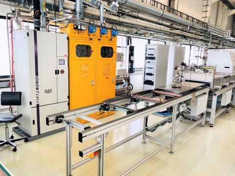
“We are very pleased with the PICOSUN® ALD system at our facilities, and all the support and consultancy we have received from Picosun over the years. With our ALD system we have been able to deposit dense, uniform ALD NiO films with low roughness and very high capacity. The excellent qualities of these films allowed us to develop high-performance anodes for SSLIBs,” says Picosun customer, Dr. Maxim Maximov from Peter the Great St.Petersburg Polytechnic University (SPbPU), Russia.

“Battery applications are yet one example of ALD’s flexibility as a method, and how new industries discover the possibilities of ALD day by day. Deep trenches with aspect ratios exceeding 1:2500 have been successfully coated with our ALD tools equipped with our patented Picoflow™ feature, which further advocates the use of our technology in 3D solid state Li-ion battery manufacturing. We are happy that our ALD solutions can be potentially utilized in future’s energy storage solutions in conjunction with clean energy production, and to power more compact healthcare devices, to improve people’s quality of life,” states Dr. Jani Kivioja, CTO of Picosun Group.

Picosun provides the most advanced ALD thin film coating technology to enable the industrial leap into the future, with turn-key production solutions and unmatched expertise in the field. Today, PICOSUN® ALD equipment are in daily manufacturing use in numerous major industries around the world. Picosun is based in Finland, with subsidiaries in Germany, North America, Singapore, Taiwan, China and Japan, offices in India and France, and a world-wide sales and support network. Visit www.picosun.com.

(*) Yury Koshtyal et. al., Atomic Layer Deposition of NiO to Produce Active Material for Thin-Film Lithium-Ion Batteries, Coatings 2019, 9, 301; doi:10.3390/coatings9050301. Open access: https://www.mdpi.com/2079-6412/9/5/301

For more information about the application of ALD in Li-ion batteries, please visit Dr. Maxim Maximov’s profile at https://www.researchgate.net/profile/Maxim_Yu_Maximov.