Friday, March 31, 2017

Forge Nano scaling up ALD on particles to metric tons level

ALD on particles and powder is a very promising next thing to shoot ahead in ALD. While many are focusing on flexible OLED barriers an backside solar cell passivation I am betting ALD on powder will take over some day - there is just much more surface area powder being shipped than windows, panels & displays (I think...) and those are flat while particles are 3D with high surface area -typical ALD arguments.

According to a recent newsletter from the Forge Nano, formerly known as PneumatiCoat Technologies, they have raised $20 million in Series A Funding. This has allowed them to move into a new 12,000 square foot facility in Louisville Colorado and scale up their 200 kg / day pilot plant to a new 1000 kg / day Semi-Continuous ALD particle coating tool.

As if that´s not amazing enough - they report to be on schedule to complete a next generation tool to a capacity to several tons per day.  

Please also do check out these fresh new US Patents and some of the cited publications :

US9,546,424 (ALD Semi-Continuous Particle Coating Process)
US9,284,643 (ALD Semi-Continuous Particle Coating Apparatus)

Wednesday, March 29, 2017

Intel announce first SAQP in Logic and Much Moore at 10 nm

Intel announce first SAQP and Much Moore at 10 nm during their most recent Investor Show (March 28, 2017). SAQP is already process of record in DRAM at Sasmung since 2016 10 nm class DRAM was introduced (LINK)


Technology Manufacturing Day - Strategy Overview (Stacy Smith)


Technology Manufacturing Day - Moore’s Law (Mark Bohr)

Technology Manufacturing Day - 14nm Leadership (Ruth Brain)


Technology Manufacturing Day - 10nm Leadership (Kaizad Mistry)


[check out slide 13, screendump]


Technology Manufacturing Day - 22FFL (Mark Bohr)


Technology Manufacturing Day - IDM Advantage (Murthy Renduchintala)


All recent briefings: LINK

April 4 2017, Atomic Scale Processing Workshop by Oxford Instruments Plasma Technology

The aim of this one-day workshop is to give an overview of current topics in the field of atomic scale processing for a range of applications. It is open to scientists and technologists working in industry and academia, with an interest in recent progress plus future trends in research and development. Participation is free but registration is mandatory. Lunch and refreshments are included. 

Date and Time : Tue, April 4, 2017, 9:00 AM – 4:00 PM CEST
Location : Minatec - Leti, Grenoble, France


Agenda: Please arrive at 8.45 for registration and coffee.
8:45-9:15 - Registration & Coffee
9:15-9:30 - Welcome & Introduction - Bernard André, Head of Materials and Technologies Department, Optronics and Photonics Division, CEA-LETI & Dr Mike Cooke, Oxford Instruments
9:30-10:00 - Atomic Layer Etch (ALE): A precision technique to enable tomorrow's technology
Dr Mike Cooke, Oxford Instruments
10:00-10:30 - Plasma etching processes at PTA using a Plasmalab 100 - Thomas Charvolin, Research engineer, INAC, PHELIQS/SINAPS laboratory
10:30-11:00 - 2D materials and ALD applications, Dr Ageeth Bol, Tue Eindhoven, NL
11:30-12:00 - Ion Beam developments in etch and deposition, Dr Sebastien Pochon, Oxford Instruments
12:00-12:30 - Atomic Layer Etch research developments at IMEC, Dr Jean-Francois de Marneffe, Senior Researcher, IMEC, Belgium
13:30-14:00 - Atomic Layer Deposition (ALD) New developments for atomic scale processing
Dr Harm Knoops, Oxford Instruments
14:00-14:30 - 2D materials fabrication technology and processes: The ‘Toolbox’ for Atomic Scale Processing, Dr Ravi Sundaram, Oxford Instruments
15:00-15:30 - Topic & speaker TBC
15:30-16:00 - Q & A session – ask the experts! Chaired by Dr Mike Cooke
16:00-16:15 - Close and networking

Saturday, March 25, 2017

Hidden Gems in the IEEE IRDS Reports and Roadmaps for ALD Folks!

This is an announcement to the ALD Folks - please be informed that the hidden gem a.k.a. the good stuff or ALD precursors are reported on in the Yield Enhancement Report and the classical "ITRS Roadmap" can be found in the More Moor Report. Please carry on with the next Super High-k, GAA FETs and 2D Materials Research!


Please also if you have input for the ALD precursor parts let me know and I will bring it up when some of us meet next time at the CMC Conference 11-12 May.


IRDS Reports

Below are links to the downloadable whitepapers.  Materials are to be shared among our industry friends. Thank you for citing the IRDS when using any materials!
This list will be updated as other IRDS whitepapers become available.

The Critical Materials Conference 2017, 11-12 May, Richardson, TX announcing Speakers

This year's Critical Materials Conference features more than 20 powerful and actionable presentations, and a highly differentiated program, with networking opportunities for all attendees. The Critical Materials Conference, a pivotal, 2-day event organized by TECHCET with the support of the Critical Materials Council, will be held this year in Richardson, Texas, on May 11th and 12th, directly following the Council Meeting. Industry experts from leading semiconductor fabricators, materials companies, and market research firms will present insights into the dynamic, and sometimes volatile, topic of semiconductor process materials and markets.


Friday, March 24, 2017

Industry ARC Webinar on Atomic Layer Deposition


Uniform ALD Al2O3 on graphene for future logic devices

TU Eindhoven and Philips Innovation Labs have just publishe a very intersteing paper on ALD of Al2O3 on prestine graphene inclusing various post deposition treatments to achive higher mobility. The trick to deposit uniform Al2O3 on graphene is by using reversible hydrogen plasma functionalization prior to ALD Al2O3 using a Oxford Instruments FlexAl PEALD reactor. Please check tha paper in Chemistrry of Materials below for more details.

Uniform Atomic Layer Deposition of Al2O3 on Graphene by Reversible Hydrogen Plasma Functionalization

René H. J. Vervuurt, Bora Karasulu, Marcel A. Verheijen, Wilhelmus (Erwin) M. M. Kessels, and Ageeth A. Bol

Chem. Mater., 2017, 29 (5), pp 2090–2100
DOI: 10.1021/acs.chemmater.6b04368


Thursday, March 23, 2017

ALD coated Minitablets help medicate picky cats

RASIRC Presents Low Temperature ALD of Titanium Nitride at MAM 2017

Company Shows Low Resistivity Results Enabled by Ultra High Purity Hydrazine

San Diego, Calif – March 23, 2017–RASIRC will present at the Materials for Advanced
Metallization conference held March 26-29, 2017 in Dresden, Germany. The poster describes an innovative chemistry for low temperature nitride films. Chief Technology Officer Daniel Alvarez will present the poster Low Temperature ALD of Titanium Nitride: Low Resistivity Enabled by Ultra High Purity Hydrazine on Monday March 27 from 13:45 – 15:30. 

MAM 2017 Conference: March 26-29, 2017 in Dresden Germany
New device architectures are driving the need for low temperature ALD methods (<400°C) to grow TiNx metal gate electrodes. TiN films require low resistivity and must be ultrathin, continuous, defect free and oxygen free. Hydrazine has very promising thermochemistry for this application but has had several challenges as well. The poster presents a method to overcome these challenges and results that show reduced flammability, reduced water contamination and improved low temperature TiNx film growth on SiON substrate.

“This new TiN metal study shows good feasibility to grow low resistivity TiNitride films at temperatures below 400C. We now have a viable alternative to plasma and high temperature ammonia,” said Jeffrey Spiegelman, RASIRC President and Founder. “This development paves the way for thermal ALD incorporation of ultrathin nitride films in 3D structured devices.”
RASIRC BRUTE® Hydrazine uses a proprietary chemical formulation to deliver ultra-high purity hydrazine from a liquid source that is safer and has quantified low water levels. The company recently released a compact Laboratory version designed for use under vacuum draw. This plug-and-play version enables universities, research institutes and smaller testing environments to work with the chemistry without changing the laboratory tools.

About Ultra High Purity Hydrazine

Alvarez will be available throughout the conference to discuss the poster and ongoing research. For more information after the conference, follow up by contacting RASIRC directly at info@rasirc.com.

About RASIRC

RASIRC specializes in products that generate and deliver gas to fabrication processes. Each unit is a dynamic gas plant in a box—converting common liquid chemistries into safe and reliable gas flow for most processes. First to generate ultra-high purity (UHP) steam from de-ionized water, RASIRC technology can now also deliver hydrogen peroxide gas and hydrazine gas in controlled, repeatable concentrations. RASIRC gas delivery systems, humidifiers, and closed loop humidification systems are critical for many applications in semiconductor, photovoltaic, pharmaceutical, medical, biological, fuel cell, and power industries. Call 858-259-1220, email info@rasirc.com or visit http://www.rasirc.com.

Contacts:

RASIRC
Jeffrey Spiegelman
Phone: 858-259-1220
E-mail: jeff@rasirc.com

Wednesday, March 22, 2017

NCD to supply Lucida GS Series ALD system to a big Chinese manufacturer, Tongwei Solar, for high efficiency crystalline solar cells

NCD has recently contracted with Chinese Tongwei Solar to supply solar cell manufacturing equipment that can produce cells of over 100MW. This equipment, Lucida GS Series ALD system, is used to process Al2O3-ALD passivation on the back side of wafers in high volume manufacturing of high efficiency crystalline solar cells.

Lucida™ GS series

The current achievement with Tongwei Solar that followed the contract from DMEGC in China means that the oversea customers have proved NCD’s technology and the excellence of the equipment once again.

Lucida GS Series as batch ALD deposition equipment can produce over 4,000 wafers (@ 6nm thickness) of 156mm X 156mm size per hour. In addition, it can operate even faster and more convenient once the system is combined with the automation that handles wafers automatically. When using our tools in solar cell production lines, the manufacturing cost will be lowered dramatically copmared to that of competitors owing to the high throughput, high yield, efficient gas consumption, and low maintenance cost of the NCD equipment.

Based on these advantages and excellence, Lucida GS Series will be the essential and international system which applies ALD process for manufacturing high efficiency solar cells in the future.

NCD’s rapid growth is expected this year because of this contract considers the green light for bulk orders. NCD does continuous efforts to be the world best and professional company leading advanced ALD technologies.

Tuesday, March 21, 2017

2016 saw growth in Multiwafer ALD Equipment due to patterning and 3DNAND

The reporting for the semiconductor equipment companies has now com to an end and reports on the development during 2016 are staring to come in. Some days ago Seeking Alpha reported on the over all situation in the Top 10 ranking as well as some insights from the companies just below, i.e., Top 20.


Based on the annual revenues reported I summarized the situation going from 2015 through 2016 in the plot above. Please find a summary and additional comments from the article below going down the ranking fro all companies relevant to ALD:

Applied Materials grew 26.2%, due to growth in 3D NAND and leading edge logic devices (FinFET) and multiple patterning processes. However, reportedly not in ALD, which remains to be confirmed. Some of that huge growth must be ALD and possibly growth fro the Olympia ALD platform.

Lam Research made a solid growth of 7.5% gaining share against Applied Materials in deposition, as its 3D NAND shipments grew more than 80%. reportedly primarily due to  growth in ALD.
Tokyo Electron was fourth, gaining 15%, primarily in CVD deposition processes. How much of this growth in CVD is actually ALD and the ratio singel/multi wafer vs. furnace was not reported. Others have claimed that Tokyo Electron is taking market share in PEALD from ASM with their NT 333 SiO2 ALD platform that relizes high speed ALD cycles to achieve system throughput of over 100 wafers per hour for e.g. SADP and SAQP. Please see a recent blog covering this tool and topic by Prof. Kessels (LINK).

 TEL NT333 High quality SiO2 ALD tool (LINK)

ASM International dropped 6.6% in 2016 due to less investments by the fabs in single wafer ALD. Single wafer ALD is mainly used for the High-k / Metal Gate Stack which until today only comes ones per wafer. ASM single wafer is also deployed for spacers and multiple patterning using the ASMI high productivity XP8 platform with dual Chambers. Apparently, the other platforms with four, five or more wafers per chamber are more productive and used for multiple passes per wafer in multi pattering and cost sensitive memory products.

Hitachi-Kokusai dropped to but remained in Top 10 loosing market chares to its furnace competitor Tokyo Electron.
Korean ALD suppliers Jusung Engineering and Wonik IPS gained market shares in ALD - how much was not reported.

Clearly the growth 2016 was in multiwafer ALD driven by patterning and 3DNAND but still a lot of question marks on the ALD situation and I look forward to the outcome from the Gartner report due soon I think.


Sunday, March 19, 2017

Beneq launched Rotary spatial plasma batch wafer ALD at SEMICON China


Sami Sneck from Beneq will presented about Rotary Spatial Plasma Enhanced Atomic Layer Deposition on Monday, 13 March, at the Shanghai International Expo Center.
  • The benefits of rotary spatial PEALD
  • µm-thick ALD films with high throughput
  • optical coating stacks by rotary spatial PEALD.

Beneq R11 offers high-perfomance ALD in a low temperature plasma enhanced process for example for multilayer anti-reflection coatings. The deposition rates are really high (µm/hour for SiO2) as is the throughput (15000 pcs of 200 mm wafers/month).

The Beneq WCS 600 roll-to-roll ALD system has been designed for demanding flexible electronics applications. It is a high-capacity industrial ALD tool for up to 500 mm wide flexible substrates. It provides continuous coating capacity of 10 nm @ 1 m/min for materials such as AI2O3.

Beneq T2S is a batch wafer tool for high capacity ALD for semiconductor applications. It offers full cassette-to-cassette automation for up to 200 mm wafers with a capacity of 20 000 wafers/month (50 nm Al2O3 ). It is ideal for LED, MEMS, and sensor applications.
[this story is a past event and will be updated when more information is available] 

 BALD Engineering talking to Beneq at ALD Ireland 2016 (Photo: Katharina Knaut)

Meyer Burger offer high-speed Spatial ALD Technology for R2R Production

Meyer Burger has updated their ALD Equipment offering and are now offering two ALD Products, one for R&D and one for Production. Both are based on Spatial ALD coating technology.

The FLEx S2S sALD


The FLEx S2S sALD is suit­able for ap­pli­ca­tion de­vel­op­ment that re­quire high speed ALD coat­ing tech­nol­ogy com­bined with ex­cel­lent uni­for­mity  (Source: Meyerburger.com)

The FLEx S2S sALD (sheet to sheet spa­tial ALD coat­ing so­lu­tion) is suit­able for ap­pli­ca­tion de­vel­op­ment that re­quire high speed ALD coat­ing tech­nol­ogy com­bined with ex­cel­lent uni­for­mity. The de­vel­oped process is trans­ferrable to the FLEx R2R sALD (roll to roll spa­tial ALD coat­ing so­lu­tion) in­dus­trial Equip­ment.

Main advantages
  • Grow rates > 1 nm/s; 100 times compared to conventional ALD
  • Flexibility in substrate material and layer thickness
  • No pinholes
  • Thickness control on atomic scale
  • No gas phase reaction. No parasitic deposition
  • Excellent conformity
  • High application potential in flexible electronics, photovoltaics, OLED
  • No vacuum process, process at atmospheric pressure
  • Compact footprint

FLEx R2R sALD'

The FLEx R2R sALD is a full scale machine for high speed production on foil.


The FLEx R2R sALD is a ALD piece of pro­duc­tion equip­ment for the de­po­si­tion of thin R2R films

Biopolymer Films Market to exceed $6bn by 2024

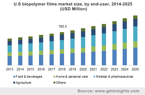
ALD is listed as one of the thin film technologies to mass produce Biopolymer thin films in a recent report "Biopolymer Films Market to exceed $6bn by 2024" by Global Market Insights Inc.
 
The US Biopolymer market segmented by Golobal Market Inc. (Source: https://www.gminsights.com/industry-analysis/biopolymer-films-market)

According to the press release Global biopolymer films market size is majorly driven by robust growth in the food & beverage industry. For instance, the global food & beverage industry is likely to observe growth close to 8% CAGR over the estimated timeframe. The industry is also positively influence by drifting consumer focus for food packaging films derived from bio-based sources such as polysaccharides (starch, cellulose) and proteins (soy, whey & gelatin). Furthermore, introduction of edible biopolymer films for the food industry will complement the overall industry share over the estimated timeframe.

“Bio-based Biopolymer Films Market is forecast to witness prominent gains of over 6% CAGR between 2016 and 2024. Abundant availability of raw materials such as cellulose, starch, pectin, chitosan, and protein will boost the global market share over the estimated timeframe.”

The product offers valued added advantages such as ecofriendly characteristics, biocompatibility and easy raw material availability. However, relatively high product cost in comparison with prevailing counterparts such as semi-synthetic and synthetic films may hamper the overall industry growth in the near future. For example, biopolymer films market price trend ranges from USD 3/kg to USD 3.5/kg. Whereas, semi-synthetic and synthetic films range from USD 1.2/kg to 2/kg.

The report includes key industry insights spread across 160 pages with 165 market data tables & 11 figures & charts from this 2017 report Biopolymer Films Market in detail along with the table of contents at: https://www.gminsights.com/industry-analysis/biopolymer-films-market


Thursday, March 16, 2017

The CMC Conference Richardson TX 11-12th May Don't Miss Out on Early Bird Registration


NEW SPEAKERS ADDED

Early Bird Registration Offered for a Limited Time*
Critical Materials Conference 2017
May 11-12 in Richardson, Texas.
Conference Vision 
The Critical Materials Conference Committee seeks to provide you with information and an experience that you can use now and for future planning. The CMC Conference provides a structured framework to catalyze the flow of "actionable" technical and supply chain information related to critical materials.  
 
Themes of the Conference are centered around the needs of the Critical Materials Council and the global IC fabrication industry. While executive conferences typically focus on the "what" and "why" of materials technologies, this conference will discuss "how" new materials can be controllably, safely, and cost-effectively used in fabs.
Keynote by Dr. Hans Stork, Sr. VP & CTO of ON Semiconductor

New Speakers Recently Added :
Linde - Paul Stockman
"Ne / Xe Demand Impact from Outside Semi applications and Reuse/Recycle challenges"
Samsung - Michael Wedlake 
"Materials and Manufacturing Challenges for Post CMP Cleaning"
Cypress - Pete Beckage
HighQ - Scott Ray
"CMP Slurry Recycling & Reuse Challenges and Strategies"

NEW blog : AtomicLimits by Prof. Kessels Group

Here is a new blog by Prof. Kessels group on nanoscience and most probably also a lot of ALD!

"AtomicLimits.com is a blog about strategy, serendipity and vision in nanoscience and it covers a variety of topics related to thin film technology (eventually lots about ALD!), semiconductor processing, nanotechnology, nanoelectronics, photovoltaics and all the like. Basically all those things that we are interested in within our research group at the Eindhoven University of Technology TU/e."

- Prof. Kessels (LinkedIn)

Screen dump form the blog (AtomicLimits.com)

Thursday, March 9, 2017

UPDATE: REGISTER NOW FOR CRITICAL MATERIALS COUNCIL (CMC) CONFERENCE 2017

‘Braking’ Through Barriers with Materials

The Critical Materials Council (CMC) Conference is a two day event providing actionable information on materials and supply-chains for current and future semiconductor manufacturing. Business drives the world, but technology enables semiconductor business, requiring us to understand the dynamics of how materials and technologies enable the scaling of devices in IC fabs. Conference speakers provide information on critical materials used in HVM fabs and look at manufacturing integration issues associated with new materials needed for future devices. Notable speakers from leading semiconductor fabricators, materials companies, and leading market research firms will provide insights on this ever-changing area of semiconductor process materials and markets.

** Register Now! **

Join the World’s Leaders


Location: DoubleTree by Hilton, 1981 N Central Expy, Richardson (near Dallas), TX 75080
Conference follows CMC Private meetings:
May 9-10, CMC Fabs
May 10, 1:30-6 pm, CMC Fabs & CMC Associates Joint Session

Keynote Presentation: Hans Stork, Sr. VP of Technology & CTO of ON Semiconductor

Three Powerful Sessions and the Not-So-Usual-Round-Table

I.  Global Issues & Supply-Chain Challenges
II.  Immediate Challenges of Materials & Manufacturing
III.  Emerging Materials Challenges: leading edge today

Attendees include industry experts who work with supply-chain management, business-development, R&D, and product management, as well as academics and analysts. CMC member companies will be attending this meeting, as it is an important part of their membership.

Wednesday, March 8, 2017

Webinar on Atomic Layer Deposition (ALD) Market Analysis

Description

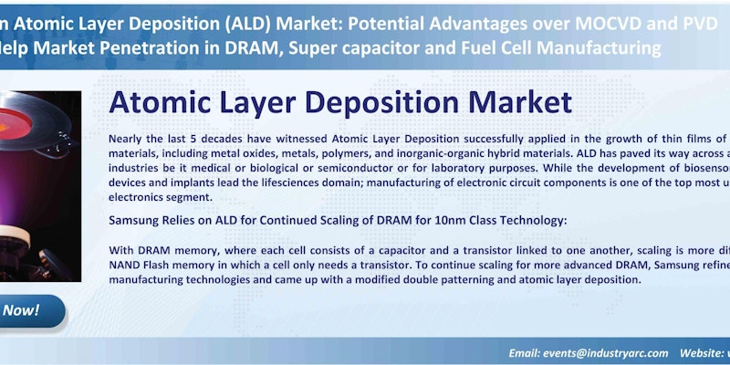
A Webbinat by IndustryARC Nearly the last 5 decades have witnessed Atomic Layer Deposition successfully applied in the growth of thin films of many classes of materials, including metal oxides, metals, polymers, and inorganic-organic hybrid materials. ALD has paved its way across a large section of industries be it medical or biological or semiconductor or for laboratory purposes. While the development of biosensors, drug delivery devices and implants lead the lifesciences domain; manufacturing of electronic circuit components is one of the top most uses of ALD in the electronics segment.

Date and Time

Thu, March 23, 2017
7:30 PM – 8:30 PM SST
Registration: LINK

Samsung Relies on ALD for Continued Scaling of DRAM for 10nm Class Technology:

With DRAM memory, where each cell consists of a capacitor and a transistor linked to one another, scaling is more difficult than with NAND Flash memory in which a cell only needs a transistor. To continue scaling for more advanced DRAM, Samsung refined its design and manufacturing technologies and came up with a modified double patterning and atomic layer deposition.

The Fuel Cell and ALD Overhaul:

ALD has clearly gained prominence in manufacture of fuel cell. IndustryARC predicts high potential in this field in the coming years. Solid Oxide Fuel Cells are noted a quality contribution to the global ALD market:

Durable and high-performance low temperature solid oxide fuel cells
ALD of ultrathin blocking layer for low-temperature solid oxide fuel cell on nanoporous substrate

Supercapacitors Manufacturing: ALD to the Rescue?

With the invent of ALD, energy conversion, producing cost competitive, durable and high performance devices have become increasingly significant and one such application is manufacture of a supercapacitor! Manufacturers, developers and suppliers of supercapacitors have lately gained utmost ascendancy. ALD encapsulated activated carbon electrodes for high voltage stable supercapacitors- continue to trend in the market.

Monday, March 6, 2017

Short course on Atomic Layer Deposition (ALD) – Eindhoven, April 20, 2017

Prof. Gregory Parsons (North Carolina State University) and Prof. Erwin Kessels (Eindhoven University of Technology) invite you to participate you in their Short course on Atomic Layer Deposition (ALD) which is aimed at people that are relatively new to the field of ALD. This includes students, technologists and other people that work – or are planning to work – on ALD but who have limited knowledge of the technology or of the underlying principles. 

 
The short course provides an introduction into ALD by providing the basics of ALD, giving an overview of the applications of ALD and describing why ALD has become so important in recent years. Insight into ALD reactors and related equipment is given and a comparison is made between ALD and other thin film techniques. Elementary aspects of precursors and precursor delivery are addressed and important information on film nucleation and other ideal and non-ideal growth effects is provided. Also, plasma and other energy-enhanced ALD methods will be described and selected cases of issues related to ALD as well as its merits will be presented.

For a full program, other information and registration, seewww.nanomanufacturing.nl/ALDcourse.

This ALD short course takes place in the framework of NanoLabNL, which is a Dutch national facility for nanotechnology research.

Speakers

Prof. Gregory Parsons (North Carolina State University, biography)
Prof. Erwin Kessels (Eindhoven University of Technology, biography)
Dr. Stephen Potts (University College London, biography)
Dr. Harm Knoops (Oxford Instruments /Eindhoven University of Technology, biography)

Picosun Expands Services and Support with Retronix

Picosun Oy, the leading supplier of advanced industrial ALD (Atomic Layer Deposition) technology, announces collaboration with Retronix Semiconductor, a well-known and highly reputed global engineering service company, to further reinforce its support and service portfolio especially for production customers.

Picosun's industrial customer base is growing fast, with increasing number of high throughput, fully automated cluster and batch production tools installed worldwide at prominent semiconductor manufacturers. To ensure always first class support tailored to every customer's individual needs, Picosun provides an all-inclusive service selection with quick lead times and comprehensive, system-specific products with competitive pricing. The services range from 24/7 support and maintenance contracts and coating service to process consultancy and advanced training programs, provided by Picosun's own Ph.D level ALD scientists, highly qualified engineers, and the company's worldwide network of distributors and representatives.

To further strengthen this service portfolio, Picosun has now signed an agreement with Retronix Semiconductor. This ensures even faster response times with highest level support for a fast growing and increasingly demanding customer base. Picosun will also continue offering support locally through current representatives and its own personnel.

"Customer happiness is essential for us at Picosun. This calls not just for the best in class ALD tools with superb process quality, but unfaltering supply, support and service chain. This is particularly emphasized on production lines where the smallest issues can easily lead to massive financial losses. We are very pleased to start collaboration with Retronix as our world-wide service partner. Their workforce of highly trained and specialized service professionals complements our service section and guarantees even better customer experience", states Dr. Erik Østreng, Applications and Services Director of Picosun.

Thursday, March 2, 2017

Hiden Analytical and Epiluvac to exhibit at EuroCVD/BalticALD in Sweden

Welcome to the Joint EuroCVD 21 – Baltic ALD 15 Conference Linköping, Sweden, 11 – 14 June, 2017. we gor a lot of abstracts and the exhibition is filling up - we have 7 more tables bofre we reach the current maximunm of 25 exhibitors - please contact us if you like to book a table!

Prof. Henrik Pedersen, Linköpings Universitet
Department of Physics, Chemistry and Biology (IFM) / Chemistry (KEMI)

Email: henrik.pedersen@liu.se
Phone: +46 13 281385

This week Hiden Analytical and Epiluvac booked tables for the exhibition and we are very happy for that. Here you can see all sponsors and exhibitors: http://www.eurocvd-balticald2017.se/


ASM International today reports its fourth quarter 2016 operating results

ASM International today reports its fourth quarter 2016 operating results (LINK)
  • Net sales for the fourth quarter 2016 were €173 million, an increase of 20% compared to the previous quarter. Year-on-year net sales increased with 19%.
  • New orders at €177 million were 44% above the Q3 2016 level.
  • Normalized net earnings for the fourth quarter 2016 increased by €29 million compared to the third quarter 2016. Operating result increased to €30 million. The financing result included €19 million positive effects from currencies compared to €3 million negative effects in the third quarter. The result from investments decreased with €8 million.


Commenting on the results, Chuck del Prado, President and Chief Executive Officer of ASM International said: "The strong overall market climate for semiconductor equipment towards the end of 2016 led to better sales and a higher order intake for Q4 than forecasted. The net cash position of ASMI remained strong. In addition to a stable proposed dividend of €0.70 per share, we announce today an increase in our current share buyback program from € 50 million to €100 million."

Outlook

  • Demand in the Logic/Foundry segment is expected to remain healthy.
  • We believe the 3D-NAND contribution to the single wafer ALD market will show a strong increase in 2017, leading to increased orders for ASMI.
  • The DRAM segment is expected to show a modest recovery in 2017.

We expect that the single wafer ALD market experienced a double digit decline in 2016. Based upon that we forecast the single wafer ALD market to reach a size of approx. US$1.5 billion in 2020-2021.

We project a year-on-year sales increase for the first half of 2017, whereby we expect a sales level of €135-145 million for Q1 and €160-200 million for Q2, both on a currency comparable level. The order intake in Q1 is expected to remain healthy at a level of €170-190 million, also on a currency comparable level.


IBM present progress in Lithography for beyond 7 nm chips at SPIE Litho

This week IBM present progress in Lithography for beyond 7 nm chips at SPIE Litho in San Diego.