


%20(1).png)
The aim of this one-day workshop is to
give an overview of current topics in the field of atomic scale
processing for a range of applications. It is open to scientists
and technologists working in industry and academia, with an interest in
recent progress plus future trends in research and development. Participation is free but registration is mandatory. Lunch and refreshments are included.
Date and Time : Tue, April 4, 2017, 9:00 AM – 4:00 PM CEST
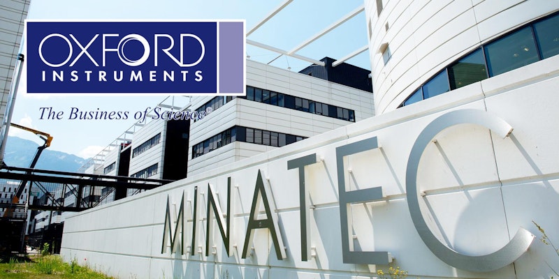
Location : Minatec - Leti, Grenoble, France
Agenda: Please arrive at 8.45 for registration and coffee.
8:45-9:15 - Registration & Coffee
9:15-9:30 - Welcome & Introduction - Bernard André, Head of Materials and Technologies Department, Optronics and Photonics Division, CEA-LETI & Dr Mike Cooke, Oxford Instruments
9:30-10:00 - Atomic Layer Etch (ALE): A precision technique to enable tomorrow's technology
Dr Mike Cooke, Oxford Instruments
Dr Mike Cooke, Oxford Instruments
10:00-10:30 - Plasma etching processes at PTA using a Plasmalab 100 - Thomas Charvolin, Research engineer, INAC, PHELIQS/SINAPS laboratory
10:30-11:00 - 2D materials and ALD applications, Dr Ageeth Bol, Tue Eindhoven, NL
11:30-12:00 - Ion Beam developments in etch and deposition, Dr Sebastien Pochon, Oxford Instruments
12:00-12:30 - Atomic Layer Etch research developments at IMEC, Dr Jean-Francois de Marneffe, Senior Researcher, IMEC, Belgium
13:30-14:00 - Atomic Layer Deposition (ALD) New developments for atomic scale processing
Dr Harm Knoops, Oxford Instruments
Dr Harm Knoops, Oxford Instruments
14:00-14:30 - 2D materials fabrication technology and processes: The ‘Toolbox’ for Atomic Scale Processing, Dr Ravi Sundaram, Oxford Instruments
15:00-15:30 - Topic & speaker TBC
15:30-16:00 - Q & A session – ask the experts! Chaired by Dr Mike Cooke
16:00-16:15 - Close and networking
No comments:
Post a Comment