Tuesday, March 31, 2015

6 Year ALD on LinkedIn

I started the ALD Group on LinkedIn six years ago in April 2009 when Qimonda the world’s 3rd largest DRAM manufacturer went down the drain. Every year I take a look at the member statistics. Growth is still steady linear cycle by cycle type of growth and today there are 2,767 members.


It is still like it has always been the case that the typical member is a Senior male Semiconductor Researcher based in San Francisco area. New is that the second biggest region representation in the group is Finland followed by Boston as number three. What has happened in the last year is that South Korea and Taiwan has overtaken the previous number two Dresden, Germany and number four Netherlands. Of course this is based on how LinkedIn organizes the world into regions.


Created: April 5, 2009
Members: 2,769
Subgroups: 5
Owner: Jonas Sundqvist (Lund University, Sweden)
Managers: Annina Titoff (ALDPulse), Riikka Puurunen (VTT Finland), Robert D. Clark (Tokyo Electron), David Thompson (Applied Materials)


SENTECH introduces PECVD / PEALD combo reactor at SEMICON China

According to a report by ALDPulse.com, SENTECH introduced a new SIPAR System at SEMICON China 2015. SIPAR combines PEALD & IC PECVD in one reactor. The SIPAR System enables automatic depositing multilayer stacks composed of plasma enhanced chemical vapour deposition (PECVD) and atomic layer deposition (ALD) layers. PECVD layers feature high deposition rates and ALD layers provide high conformity and homogeneity. SIPAR is designed for low damage deposition of multilayers at low temperature <100°C using the SENTECH proprietary PTSA inductively coupled plasma source.

http://www.sentech.com/files_db/1413800282_0324__14_medium.jpg
 
The SIPAR Chamber was first introduced on the German market at the ThGOT workshop in Leipzig late 2014.

"New system for PEALD & ICPECVD in one reactor presented at ThGOT"

Sunday, March 29, 2015

ALD on Youtube by ALDPulse

ALDPulse.com has collected the best overview of ALD Movies that are available on Youtube and sorted them in a nice way. Together with the own material in the form of Skype Interviews with ALD People this is the best page to get started with ALD.

https://www.youtube.com/user/ALDPulse?feature=guide

Check out the ALDPulse way for much more information on ALD. Here are my favourites:

ALD R&D Equipment Chart

This chart will be subject to updates according to audience and each companies' feedback and input, more companies and criteria may be added in the future.

ALD Around The World

ALDPulse keeps track of all ALD labs in the world - just get in contact with them if you lab is missing. You can email them at info@aldpulse.com

http://www.aldpulse.com/


Saturday, March 28, 2015

Electrostatic supercaps by ALD anodic alumina for energy harvesting [OPEN ACCESS]

Development of electrostatic supercapacitors by atomic layer deposition on nanoporous anodic aluminum oxides for energy harvesting applications [OPEN ACCESS]
Lucía Iglesias, Víctor Vega, Javier García, Blanca Hernando and Víctor M. Prida
Front. Phys., 25 March 2015 | doi: 10.3389/fphy.2015.00012

http://www.frontiersin.org/files/Articles/134710/fphy-03-00012-r2/image_m/fphy-03-00012-g001.jpg 

Schematic view of the cross section of the supercapacitor engineered onto the NAAM indicating the CDC layered structure and defining the lattice parameters involved in the capacitance calculation. Conductive layers of AZO are in red and dielectric layer of alumina in brown. Outlined are the 3 different contributions to total capacitance of the-designed supercapacitor prototype.

Nanomaterials can provide innovative solutions for solving the usual energy harvesting and storage drawbacks that take place in conventional energy storage devices based on batteries or electrolytic capacitors, because they are not fully capable for attending the fast energy demands and high power densities required in many of present applications. Here, we report on the development and characterization of novel electrostatic supercapacitors made by conformal Atomic Layer Deposition on the high open surface of nanoporous anodic alumina membranes employed as templates. The structure of the designed electrostatic supercapacitor prototype consists of successive layers of Aluminum doped Zinc Oxide, as the bottom and top electrodes, together Al2O3 as the intermediate dielectric layer. The conformality of the deposited conductive and dielectric layers, together with their composition and crystalline structure have been checked by XRD and electron microscopy techniques. Impedance measurements performed for the optimized electrostatic supercapacitor device give a high capacitance value of 200 μF/cm2 at the frequency of 40 Hz, which confirms the theoretical estimations for such kind of prototypes, and the leakage current reaches values around of 1.8 mA/cm2 at 1 V. The high capacitance value achieved by the supercapacitor prototype together its small size turns these devices in outstanding candidates for using in energy harvesting and storage applications.
 
http://www.frontiersin.org/files/Articles/134710/fphy-03-00012-r2/image_m/fphy-03-00012-g007.jpg
 
(A) TEM top view image of a planar section of the sample structure after being carefully prepared for displaying the nanopores after depositing the CDC structure. (B) TEM image showing the different CDC layers constituting the supercapacitor: BE and TE of AZO layers are represented in red color and the Al2O3 dielectric layer in green. (C) STEM image and (D) compositional analysis along the line-scan profile of the pore indicated in (C), where it is clearly evidenced the presence of three elements [zinc (blue), aluminum (red) and oxygen (green)], which spatially match with the CDC structure deposited on the NAAM.

PEALD Publication Histograms for 2014 by The Plasma-ALD-Guy


The Plasma-ALD-Guy has created a histogram of the regions which have produced plasma ALD publications that were accepted during 2014. The region for a paper is determined from the first author affiliation (here). In addition, he has compiled a similar histogram for Plasma ALD Film Type also for 2014 Publications (here). Both are reproduced below with permission.


Knowing that both BENEQ and Picosun are manufacturing and shipping PEALD reactors the low number of Finnish PEALD publications is surprising. No surprise though that USA and South Korea is pumping out PEALD publications and that many of them are for classic materials like Al2O3 and SiO2 and also for AlN that is just about impossible to realize in thermal mode.

The Plasma-ALD-Guys tells me that there are more publication histograms to come and I am very eager to see those - stay tuned for more!


Brown University uses silicon telluride to produce multilayered two-dimensional semiconductor materials


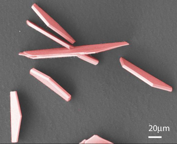
 By adjusting the fabrication technique, researchers can make different semiconductor structures, including nanoplates that lie flat or stand upright. Koski lab/Brown University
 
A Silicon-Based Two-Dimensional Chalcogenide: Growth of Si2Te3 Nanoribbons and Nanoplates
Sean Keuleyan , Mengjing Wang , Frank R. Chung , Jeffrey Commons , and Kristie J. Koski
Department of Chemistry, Brown University, Providence, Rhode Island 02912, United States
Nano Lett., Article ASAP
DOI: 10.1021/nl504330g

Abstract Image

We report the synthesis of high-quality single-crystal two-dimensional, layered nanostructures of silicon telluride, Si2Te3, in multiple morphologies controlled by substrate temperature and Te seeding. Morphologies include nanoribbons formed by VLS growth from Te droplets, vertical hexagonal nanoplates through vapor–solid crystallographically oriented growth on amorphous oxide substrates, and flat hexagonal nanoplates formed through large-area VLS growth in liquid Te pools. We show the potential for doping through the choice of substrate and growth conditions. Vertical nanoplates grown on sapphire substrates, for example, can incorporate a uniform density of Al atoms from the substrate. We also show that the material may be modified after synthesis, including both mechanical exfoliation (reducing the thickness to as few as five layers) and intercalation of metal ions including Li+ and Mg2+, which suggests applications in energy storage materials. The material exhibits an intense red color corresponding to its strong and broad interband absorption extending from the red into the infrared. Si2Te3 enjoys chemical and processing compatibility with other silicon-based material including amorphous SiO2 but is very chemically sensitive to its environment, which suggests applications in silicon-based devices ranging from fully integrated thermoelectrics to optoelectronics to chemical sensors.

Friday, March 27, 2015

Tuning the nanopore diameter using ALD

Working on deep deep nano holes and tubes for a long time (DRAM) and for a lab growing nanowires I found this an interesting paper on how ALD can be used to tune the nanopore diameter. Nanopore (NP) technologies have been researched the last 10 years or so. According to the paper "The next major breakthrough" of this technology will depend on :
  • the fundamental understanding of the dynamical processes that govern macromolecules translocation through NP
  • the availability of methods that allow routine fabrication of nanoscale materials. 
Particles, holes, tubes, wires, pores, ..., transistors etc. - what else could you do nano?

Influence of nanopore surface charge and magnesium ion on polyadenosine translocation

Mathilde Lepoitevin, Pierre Eugène Coulon, Mikhael Bechelany, Julien Cambedouzou, Jean-Marc Janot and Sebastien Balme
Mathilde Lepoitevin et al 2015 Nanotechnology 26 144001
doi:10.1088/0957-4484/26/14/144001

We investigate the influence of a nanopore surface state and the addition of Mg2+ on poly-adenosine translocation. To do so, two kinds of nanopores with a low aspect ratio (diameter ~3–5 nm, length 30 nm) were tailored: the first one with a negative charge surface and the second one uncharged. It was shown that the velocity and the energy barrier strongly depend on the nanopore surface. Typically if the nanopore and polyA exhibit a similar charge, the macromolecule velocity increases and its global energy barrier of entrance in the nanopore decreases, as opposed to the non-charged nanopore. Moreover, the addition of a divalent chelating cation induces an increase of energy barrier of entrance, as expected. However, for a negative nanopore, this effect is counterbalanced by the inversion of the surface charge induced by the adsorption of divalent cations.


Cartoon to illustrate polyA translocation through NP and the electrolyte distribution. (a) Native -NP at NaCl 150 mM (b) native-NP at NaCl 500 mM and (c) TMS-NP at NaCl 150 mM.

Check out The Nanopore Site!

http://www.thenanoporesite.com/