Thursday, June 30, 2022

Back to Basics: Understanding Conformality with Riikka Puurunen – ALD Stories Ep. 14

Back for her second episode, Professor Riikka Puurunen is bringing us back to the basics with a deep dive on conformality. Recorded live from the Harald Herlin Learning Center at Aalto University, Tyler and Riikka talk about the all-important property of ALD. In this episode, Riikka explains the history of conformality in ALD, her recent paper on modeling collaboration, the origins of the PillarHall conformality test structures, and a conversation on open science.


One question came up, when was ALD first used for high aspect-ratio DRAM capacitors? It was 2004 by Samsung Samsung begins making DRAMs on 90-nm process - EETimes

Chipmetrics has commercialized the PillarHall test chip and more information can be found here: Chipmetrics

PillarHall – introduction in SlideShare

PillarHall – introduction in YouTube

PillarHall – short introduction in YouTube

Video: How to use PillarHall test chip

PillarHall Web Site


Chipmetrics at ALD 2022 in Ghent.


Monday, June 27, 2022

ALD/CVD Precursor Markets – Burgeoning Applications

Advanced Logic and Memory Applications require more deposition materials.

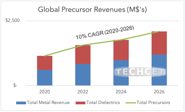
San Diego, CA, June 27, 2022: TECHCET—the electronic materials advisory firm providing business and technology information— reports that the Total ALD/CVD precursor market grew 21% in 2021, reaching US$1.39 billion and is forecasted to grow 12% in 2022. The 2022 Precursor market will top US$1.56 billion due to strong industry growth overall, driven by higher production volumes of < 7nm logic devices and higher increased stacking and layers in 3DNAND devices. The transition to EUV lithography for DRAM fabrication will also result in opportunities for increased precursor revenues. More details on these market trends will be revelaed in TECHCET’s presentation given at the 2022 ALD Conference, starting this week in Ghent, Belgium, by Jonas Sundqvist, Ph.D., or can be found in TECHCET’s newly released Critical Materials Reports™ on ALD/CVD Metal Precursors and Dielectric Precursors.


“ALD and CVD are a materials and chemistry rich industry segment with major development efforts in place, with strong prospects for growth, and for the need of new materials”, states Jonas Sundqvist, Sr. Technology Analyst at TECHCET. “New manufacturing solutions designed to meet both cost and performance will rely on ALD precursor materials.”

New materials and related process technologies are being driven by changes in device design. For advanced logic, new precursors are required for transistors to form high-κ gate dielectrics, metal gate electrodes, strain/stress epi of the channel and channel materials. DRAM memory cells continue pushing for higher-κ capacitors. And advanced devices, especially logic, demand improved interconnect wiring, barriers, seed layers, selective via capping and encapsulation, insulators, as well as new and/or more dielectrics to support EUV and advanced ArFi photolithography.

Emerging challenges persist as a result of continued dimensional scaling addressed with materials, especially new materials deposited by ALD. Area selective deposition has been a trend in the past 5 years with a growing R&D community to implement this approach in future devices.

For device specific details on the ALD/CVD Precursor markets & segments get TECHCET’s newly released Critical Materials Report™ here: https://techcet.com/product-category/ald-cvd-precursors/

Friday, June 24, 2022

Hydrogen Peroxide Gas on the road from R&D to HVM for superior HZO films

Device shrinkage, three-dimensional and High Aspect Ratio (HAR) structures, and lower thermal budgets drive the continued search for new materials. A by-product of this search is a need for better oxidants for atomic layer deposition (ALD) and other thin film deposition processes.

While metal usage is rapidly expanding across the periodic table, oxidant choices are few: water, O2, ozone, and oxygen plasma being the leading choices for thin-film processing.

Each oxidant has its strengths and weaknesses. Plasma has limitations with the line of sight and may damage underlying sensitive channel materials or metal interconnects. Ozone is too aggressive with most metals. Water and oxygen are not reactive enough for today’s lower thermal budgets and more demanding precursors. Therefore, new oxidants could help address low-temperature thermal applications and simplify precursor design and selection.

At RASIRC, the investigation began for alternative oxidants when water vapor proved too limited for many ALD applications. Interest in delivering gas generated from hydrogen peroxide liquid began in 2007, with the first commercial sales in 2011 and 2012.

While the perception of the semiconductor industry is one of rapid innovation, the adoption of new technology is a slow process. If successful, it can frequently exceed a decade to reach high volume manufacturing.

Recently, RASIRC presented (April 2022 CMC2022, AZ, USA) benchmarking hydrogen peroxide vs. water and ozone in ALD of ferroelectric hafnium zirconium oxide (HZO). HZO is one of the primary candidate materials for new non-volatile memory using a capacitor device; it can be integrated into both Logic devices and as a stand-alone memory chip similar to Flash memory.

RASIRC and UT Dallas fabricated capacitor structures (MIM) and deposited HZO using water, ozone, or hydrogen peroxide at comparable process conditions.

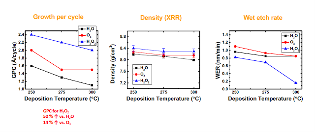
The first finding was that the growth rate per cycle (GPC, below left) was considerably higher in the hydrogen peroxide case, essentially lowering the overall process time and precursor consumption of rather expensive Hafnium and Zirconium precursors. The hydrogen peroxide HZO films also proved to have a higher density (XRR, below middle) and lower etch rate (wet etch rate below right).


Growth rate per cycles, density by X-ray Reflectivity (XRR) and wet etch rate determination of HZO films deposited by ALD using either hydrogen peroxide, water or ozone.

Higher density metal oxide films are a sure sign of better electrical performance regarding high-k dielectrics and ferroelectrics. First, the hydrogen peroxide films showed a comparably higher effective k-value, lower leakage current (Jg), and could withstand a higher breakdown voltage (VBD), as seen below right. Water results were inferior to both ozone and hydrogen peroxide are not shown for clarity.

Indicative for ferroelectric phase content is a peak at approx. 2T= 30.3 deg and 35.8 (below right). In X-ray diffractograms, when comparing hydrogen peroxide vs. ozone, it[JS1] was shown that the hydrogen peroxide films could show a higher orthorhombic (ferroelectric) phase content at a lower thermal budget, i.e., the onset temperature for crystallization. Even though the orthorhombic ferroelectric phase is metastable over preferred tetragonal and monoclinic HfO2 and ZrO2 most stable phases, this can be understood that the atoms in higher density and purer hydrogen peroxide films will find their optimum positions under given conditions in the lattice faster due to less disturbance from contamination species that has to diffuse out of the lattice before a ferroelectric phase content can crystalize quenching the HZO films into the metastable ferroelectric phase.


Leakage (Jg) vs breakdown voltage (VBD) and gracing incidence x-ray diffraction (GI-XRD) after post deposition anneals for hydrogen peroxide HZO films compared to ozone HZO films.

The promising results above for higher quality ferroelectric films were then proven by complete ferroelectric electric characterization sweeping the current and voltage across the capacitor structures accordingly. As seen below in the P-E hysteresis curves, a clearly defined hysteresis response curve could be verified for hydrogen peroxide HZO films at a lower RTA temperature than for ozone films, the onset of 325 vs. 350 deg C. It may seem like a slight difference, but please keep in mind that the overall thermal budget for device integration in copper interconnect layers is in the range 350 to 390 deg.C depending on layer and technology node, and it is critical to stay below this temperature and as can be seen below this study yielded beautiful ferroelectric hysteresis at 350 deg. C for hydrogen peroxide, whereas ozone films had to go up to the danger zone of 400 deg. To do the same.
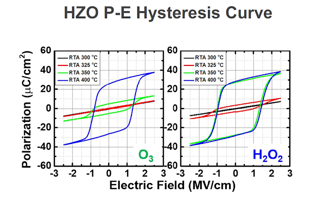
P-E hysteresis curves for hydrogen peroxide (right) and ozone (left) ferroelectric HZO films for different RTA thermal budgets.

Finally, TEM analysis showed that films could be downscaled to 5 nm film thickness and most probably below, staying perfectly intact even though a high roughness metal bottom electrode was used. 


High-resolution transmission electron microscopy (HR-TEM) of ferroelectric HZO films deposited by ALD and using RASIRC hydrogen peroxide technology.

To conclude, HZO ferroelectric films showed many advantages when hydrogen peroxide was employed compared to water and ozone:

· Higher device yield as measured in the number of functional ferroelectric capacitors

· Higher density films with lower wet etch rate

· Higher effective k-value

· Faster growth (ALD GPC)

· Lower film thickness for yielding films in electrical testing

· Lower leakage current and higher breakdown voltage

· Crystallization onset for ferroelectric phase content for lower thermal budgets (RTA temperature)

Next you can meet RASIRC at the AVS 22nd International Conference on Atomic Layer Deposition (ALD 2022), will be a three-day meeting 26-29th of July in Ghent Belgium, dedicated to the science and technology of atomic layer-controlled deposition of thin films and now topics related to atomic layer etching. Jeff Spiegelman, CEO of RASIRC will be presenting “Higher Effective Dielectric Constant of Hafnium Oxide When Grown with Hydrogen Peroxide Compared to Water Vapor” in session AF-MoP18 on 27th of June.

About RASIRC

RASIRC transforms liquids into dynamic gases that power process innovation in semiconductor and adjacent markets. By commercializing molecules for lower temperature processes, RASIRC patented technology enables the manufacture of atomic-scale oxides, nitrides, and metals. Innovative products such as BRUTE Peroxide, BRUTE Hydrazine, the Peroxidizer®, and Rainmaker® Humidification Systems are being used to develop solutions for 5G, AI, IOT, and advanced automation.

What makes RASIRC a unique industry leader is our technical expertise and commitment to solving complex industry challenges for our customers. Our team of industry experts has a proven track record of being first to market by efficiently delivering state of the art technology that reduces cost, improves quality, and dramatically improves safety. With our customers at the forefront of all we do, we continue to research, develop, and design innovative products that purify and deliver ultra-pure gas from liquids for the semiconductor and related markets. Contact RASIRC to help solve your complex problems. P: 858-259-1220, email info@rasirc.om or visit http://www.rasirc.com

Thursday, June 23, 2022

TANAKA Establishes New Ruthenium Film Deposition Process That Contributes Toward Improved Durability Of Semiconductors

TANAKA Kikinzoku Kogyo K.K. (Head office: Chiyoda-ku, Tokyo; Representative Director & CEO: Koichiro Tanaka), which operates the TANAKA Precious Metals manufacturing business, announced today that TANAKA has established a two-stage film deposition process using the liquid ruthenium (Ru) precursor "TRuST." TRuST is a precursor that has excellent reactivity with both oxygen and hydrogen and can form high-quality ruthenium films. This process is a two-stage atomic layer deposition (ALD) process that uses hydrogen film formation to create a thin anti-oxidation film and oxygen for the deposition of a high-quality ruthenium film. It eradicates concerns that the substrate will become oxidized and, at the same time, can prevent the drop in ruthenium purity that occurs during hydrogen film deposition


The film deposition process was proposed by Professor Soo-Hyun Kim from the School of Materials Science and Engineering, College of Engineering, Yeungnam University in South Korea. The development and evaluation of the film deposition process were jointly conducted by Professor Kim and TANAKA Kikinzoku Kogyo.

This technology is expected to achieve greater miniaturization and improved durability of semiconductors. It can therefore be expected to be used in data centers and smartphones - which require even greater data processing capabilities - and contribute toward advanced technologies such as IoT and autonomous driving, which require sophisticated technological innovations.

Two-Stage Film Deposition Process Using Oxygen And Hydrogen

TANAKA Kikinzoku Kogyo is developing high-purity precious metal precursors centered on ruthenium for next-generation semiconductors. So far, single-stage film deposition using oxygen has been the mainstream process for film deposition. However, the company has now succeeded in a two-stage film deposition process using oxygen and hydrogen.

This two-stage film deposition process reduces the risk of surface oxidation of the base caused by hydrogen film deposition and allows high-purity film deposition that maintains ruthenium purity at almost 100% using oxygen film deposition. Furthermore, by forming the base first using hydrogen film deposition, the ruthenium film on top of the base created using oxygen film deposition will be smooth and dense, achieving a lower resistance than before.

Generally, specific resistivity increases when film thickness decreases, which is an issue in film deposition of semiconductors. With this new process, it was confirmed that an even lower resistance results from a two-stage film deposition that uses hydrogen in addition to oxygen film deposition, especially in the range of 10 nm and below. As semiconductors become even smaller in scale in the future, demand for thinner film deposition with low resistance is also expected for ruthenium films, and a two-stage film deposition allows this issue to be resolved. In addition, the new low-resistance, high-purity ruthenium film created by the two-stage film deposition can be achieved using the same raw materials and film deposition temperature for both stages. Therefore, film deposition is possible using the same film deposition equipment, allowing capital investment costs to be suppressed. Details will be announced at the AA2-TuA: ALD for BEOL session of the ALD 2022 conference being held in Ghent, Belgium, on June 28, 2022.

TANAKA Kikinzoku Kogyo's Liquid Ruthenium Precursor "TRuST"

In the past, the most common thin film and wiring materials used for semiconductors were copper, tungsten, and cobalt, but there are increasing expectations for the precious metal ruthenium to promote greater miniaturization of semiconductors because of its lower resistance and higher durability. Therefore, TANAKA Kikinzoku Kogyo developed TRuST - a liquid ruthenium precursor for chemical vapor deposition (CVD) and ALD that achieved the world's highest vapor pressure value - and started providing samples in 2020.

By increasing to the world's highest vapor pressure value, which is more than 100 times higher than existing precursors, this precursor raises the concentration of precursor in the film deposition chamber and the adsorption density of precursor molecules on the substrate surface, achieving excellent step coverage and improved film deposition speed.

State of the Semiconductor Industry and Background

The progress of advanced technologies such as IoT, AI, 5G, and the metaverse has led to rapidly increasing volumes of digital data used by digital devices such as smartphones. Therefore, in the development of semiconductors, the need for even greater miniaturization is increasing to enable the creation of devices with higher performance and lower energy consumption. In the aspect of durability, degradation due to base oxidation is also a major issue in semiconductor development. Furthermore, the development of electric vehicles and self-driving cars requires similar needs for the miniaturization of automotive semiconductors along with further improvement in durability.

In the semiconductor industry, which will require greater miniaturization and improved durability in the future, TANAKA Kikinzoku Kogyo seeks to further reduce costs and achieve higher quality by improving the film deposition speed of liquid ruthenium precursors. At the same time, the company will contribute to greater miniaturization and improved durability of semiconductors to support the development of new advanced technologies enabled by semiconductors.

How Forge Nano is Engineering the Future, One Atom at a Time

Utilizing proprietary nano-coating technology, Forge Nano is able to fundamentally improve nearly any material on earth at the atomic level.

THORNTON, Colo., June 23, 2022 (Newswire.com) – Forge Nano, leaders in atomic layer deposition (ALD) technology and equipment, are working to unlock the next generation of materials science. Through a full product line of ALD equipment addressing large scale manufacturing all the way down to fundamental R&D, Forge Nano has developed nano-coating solutions that are cost-effective, and can improve nearly any product from the atoms up.

“For decades, ALD has been relegated to bench-top exercises and the world of peer-reviewed articles,” says James Trevey, Ph.D., CTO of Forge Nano. “It’s like we’re selling wireless internet in a world of Cat 5 ethernet cables. ALD delivers greater performance for a lower cost than incumbent technology for nearly any application, and now we have brought this technology to the commercial environment at true manufacturing scale.”


Atomic Layer Deposition (ALD) is a surface engineering technique whereby an extremely thin coating (as thin as a single layer of atoms) is applied to a wide range of materials, powders, or objects. This process can be repeated to build up multiple layers on nearly any surface, producing robust coatings that can be engineered to enhance or add to the characteristics of the material being coated.

Conventional coating techniques such as physical vapor deposition (PVD) and chemical vapor deposition (CVD) have been the standard techniques used in many industries in the past, but as ALD is now available for any material at commercial scale, their time is limited. Forge Nano’s team of scientists and engineers have developed a line of ALD tools that make the technology cost-effective and practical to apply in small-scale lab environments all the way up to full-scale commercial manufacturing settings. Case in point – Forge Nano has already demonstrated commercial success in many markets, including batteries, pharmaceuticals, and semiconductors.

Batteries – Making better, longer lasting, safer batteries

Forge Nano ALD coatings have been demonstrated to improve energy density, lifetime, safety, and cost of batteries. In an electric vehicle these benefits would translate to a lower cost, longer range, faster-than-fuel recharge times, and an EV battery that can last for at least 20 years and is better suited for recycling than current EV batteries. Forge Nano’s ALD techniques have also been shown to be more cost effective, more efficient, more precise, and more environmentally friendly than batteries made with other coating techniques.

Pharmaceuticals – Imagine controlled, single-dose, temperature-stable vaccines that can be effectively distributed around the globe without the fear of spoilage.

Forge Nano ALD coatings have been used by pharmaceutical companies to apply various characteristics to medications or vaccines. ALD coatings can make a vaccine thermostable, eliminating the need for refrigeration. Time release properties can be applied as well, allowing multiple doses to be combined into a single treatment or injection. This can make the medication or vaccine easier to distribute to rural areas and eliminates the need for additional doses or boosters.

Semiconductors – Optimizing Next-Gen devices at the atomic scale.

Forge Nano ALD coatings can be applied to semiconductor wafers and components to create hermetic, pin-hole free, low stress thin films that offer excellent uniformity and precision required by semiconductor manufacturers. In addition to producing superior coatings, Forge Nano tools can produce ALD coatings faster and more efficiently than anyone else, making Forge-enabled semiconductors

Thanks to the scalability of Forge Nano’s extensive research and development, ALD technology that was once thought of as too expensive is now accessible and practical even at the smallest of scales. Forge Nano is using its manufacturing expertise to provide R&D equipment to universities, national labs, and centers of excellence, establishing ALD as a viable commercial pathway for materials science researchers. This is contrasted by the many companies Forge Nano has worked with to integrate ALD into their manufacturing processes, installing high-volume equipment capable of coating enormous amounts of materials, powders or objects.

For those not ready to make the investment in Forge Nano’s ALD equipment, R&D and toll coating services are available as well. Forge Nano offers their world-class ALD technical team to develop coating solutions and run proof of concept tests. Forge Nano is also uniquely equipped to offer toll coating services, where an organization may entrust Forge Nano to produce the ALD coatings with their in-house equipment.

To find out more about Forge Nano’s proprietary atomic layer deposition (ALD) processes and equipment, visit ForgeNano.com.

Wednesday, June 22, 2022

Solar Energy Research Institute of Singapore (SERIS) Opts for SALD

The Solar Energy Research Institute of Singapore (SERIS) gears up perovskite solar cells for industrial tandem cell production

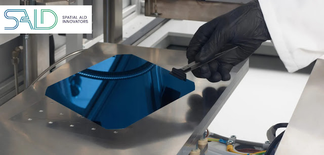
Eindhoven/Netherlands, Singapore, 18 June 2022 - The Solar Energy Research Institute of Singapore (SERIS) at the National University of Singapore (NUS) announces that it will upgrade its "Spatial Atomic Layer Deposition" (SALD) equipment. SoLayTec and SERIS have been working closely together for over a decade in the field of silicon solar cells. Now, SERIS states that SoLayTec will upgrade its existing ALD system using the latest technology of SALD BV, a Dutch technology start-up, for development of scalable perovskite-silicon tandem solar cells.


"Upgrading to the new SALD equipment brings us significant advantages," explains Dr. Shubham Duttagupta, Deputy Director of the Next-Generation Industrial Solar Cells & Modules Cluster at SERIS. The Dutch company SALD BV has developed a unique, patented technology for applying precise coatings on an industrial scale that can be as thin as a single atom. These so-called nanocoatings are promising to revolutionize numerous industrial manufacturing processes, and thus entire branches of industry. In the solar industry, SALD coatings are key for perovskite-silicon tandem solar cells, which can achieve efficiencies far above the theoretical limit of silicon-only solar cells, which are the most widely used solar cells today. It is precisely in this new area where SERIS aims to use the new SALD technology. Thanks to the SALD process, new solar cell materials can be used, including tin oxide and transparent conductive oxides, as well as novel passivation and tunnel recombination layers. The technologies developed by SERIS will be made available to industrial solar cell manufacturers through licensing agreements.


Perovskite solar cells are highly efficient, easy to process and inexpensive to produce, but still face technical challenges regarding their long-term stability. An atomically thin coating, as can be achieved with the SALD technology, makes the cells significantly more robust. SERIS wants to take the leap “from lab to fab”, i.e., from the laboratory environment to large-volume production with the new SALD machine. The potential for perovskite-silicon solar cells is great: According to forecasts, the global market is expected to exceed two billion dollars by 2027.

SALD BV has developed a unique worldwide patented technology for applying coatings that are as thin as a single atom on an industrial scale, termed "Spatial Atomic Layer Deposition" or SALD (www.spatialald.com). These atomically-thin coatings can bring revolutions to entire industries, such as the manufacturing of batteries for cars and smart devices, and the solar energy industry.

Further information: SALD BV, PO Box 520, 5600 AM Eindhoven, The Netherlands,
Web: www.spatialald.com, E-Mail: info@spatialald.com, Tel: +31 40 23 80 500,

contact: Lonneke van Wel, Tel. +31 40 238 05 00, E-mail: lonneke.vanwel@spatialald.com

PR-Agent: euromarcom public relations, Tel. +49611-973150, E-Mail: team@euromarcom.de, Internet: www.euromarcom.de, www.facebook.com/euromarcom (like if you like-:)

NCD supplied ALE and ASD equipment to Samsung Electronics Co., Ltd.

NCD has recently supplied ASD (Area Selective Deposition) equipment to Samsung Electronics Co., Ltd. Following ALE (Atomic Layer Etching).

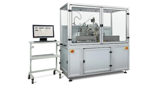
This is the cluster system which consists of two process modules (PMs) and a wafer transfer module (TM) and applies a running program for process integration. In addition, it is equipped to process at high temperatures up to 500℃ and process with ozone and plasma for developing the next semiconductor devices.

ALE is able to etch a deposited layer by atomic scale as opposed to ALD and ASD can only deposit on the selective area not grow the whole area of substrates by ALD.

Today, lots of universities, institutes, and companies have actively been developing future high-tech and highly integrated devices using ALE and ASD processes.

NCD expects that the ALE/ASD system will contribute very much to the development of high-end semiconductor technology and is going to do all of the efforts to the best ALD equipment company with new challenges and continuous R&D.

<Lucida M200PL Series ALD System>


Thursday, June 16, 2022

Applied Materials Broadens its Technology Portfolio for Specialty Chips with Acquisition of Picosun

SANTA CLARA, Calif., June 16, 2022 – Applied Materials, Inc. today announced it has acquired Picosun Oy, a privately held semiconductor equipment company based in Espoo, Finland. Picosun is an innovator in atomic layer deposition (ALD) technology, primarily for specialty semiconductors.


As electronic products become smarter and more connected, they require greater numbers of specialty semiconductors built on non-leading-edge process nodes. Applied’s ICAPS (IoT, Communications, Automotive, Power and Sensors) group provides materials engineering solutions to customers in these growing markets. The addition of Picosun’s ALD technology broadens the Applied ICAPS product portfolio and customer engagements. Picosun also brings to Applied deep R&D capabilities, talented teams and strong relationships with leading research institutions and universities throughout the world.

“Picosun is a pioneer in ALD technology with products that serve fast-growing segments of the specialty foundry-logic market,” said Gary Dickerson, President and CEO of Applied Materials. “The addition of Picosun complements Applied Materials’ technology portfolio and expands our opportunities to accelerate our customers’ roadmaps.”

“Rapid growth in the number of connected devices is driving a tremendous need for innovation in the chips used to bridge the analog and digital worlds,” said Sundar Ramamurthy, Group Vice President and General Manager of the ICAPS group at Applied Materials. “Bringing Picosun’s talented team to Applied Materials will strengthen our ability to help customers add more intelligence and functionality to a wide variety of edge computing devices.”

“Picosun has a strong history of innovation, with roots dating back to the invention of ALD technology nearly 50 years ago,” said Kustaa Poutiainen, Former Chairman of the Board of Picosun. “As we look ahead to our next phase of growth, we believe starting a new journey as part of Applied Materials – a company we have long admired – is the best path forward and will create exciting opportunities for our employees, customers and research partners.”

The Picosun team will continue to be based in Finland and will report into Applied’s ICAPS group.

The transaction has been approved by the Ministry of Economic Affairs and Employment of Finland; no other regulatory approvals were required. Financial terms of the transaction were not disclosed.

Goldman Sachs & Co. LLC served as financial advisor and Hogan Lovells US LLP served as legal counsel for Applied Materials.

About Applied Materials

Applied Materials, Inc. (Nasdaq: AMAT) is the leader in materials engineering solutions used to produce virtually every new chip and advanced display in the world. Our expertise in modifying materials at atomic levels and on an industrial scale enables customers to transform possibilities into reality. At Applied Materials, our innovations make possible a better future. Learn more at www.appliedmaterials.com.

About Picosun

Picosun provides the most advanced ALD (Atomic Layer Deposition) thin film coating solutions for global industries. Picosun’s ALD solutions enable a technological leap into the future, with turn-key production processes and unmatched, pioneering expertise in the field – dating back to the invention of the technology itself. Today, PICOSUN® ALD equipment are in daily manufacturing use in numerous leading industries around the world. Picosun is based in Finland, with subsidiaries in Germany, USA, Singapore, Japan, South Korea, China mainland and Taiwan, offices in India and France, and a world-wide sales and support network. Visit www.picosun.com.

Electronic Gases Markets – To Approach a US$9 Billion Market in 2022

New materials and increasing chip design complexity drives supply-chain problems for Specialty Gases, Rare Gases and Helium

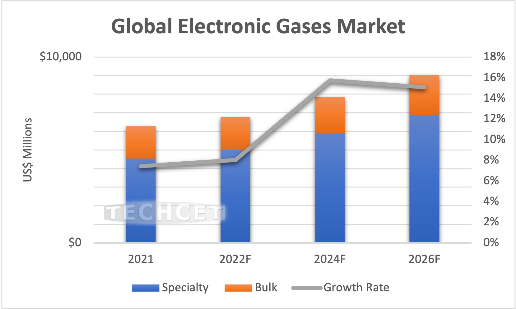
San Diego, CA, June 15, 2022: TECHCET—the electronic materials advisory firm providing business and technology information— reports that the Electronic Gases market revenues hit US$6.3 billion in 2021 and is forecasted to grow to 8% in 2022. In its recently completed Electronic Gases Report , TECHCET forecasts the 2022 Electronic Gases market will reach almost US$6.8 billion—growth primarily attributed to Specialty Gases. As leading-logic and new generations of memory continue to ramp, Specialty Gases consumed in etching, deposition, chamber cleaning, and other applications remain in strong demand. This segment is forecasted to increase by 10% in 2022 with ~9% CAGR through to 2026, as indicated in TECHCET’s newly released 2022 Critical Materials Report™ on Electronic Gases, authored by Jonas Sundqvist, PhD.


In the near-term, there are supply issues for key industry gases, such as helium and neon; and in the longer term, the supply/demand balance for gases such as nitrogen trifluoride (NF3), tungsten hexafluoride (WF6), and others could tighten as industry demand grows.

Neon supply capacity is at risk due to the Russian invasion of Ukraine. Some gas supply from these sources may be at a permanent loss. Helium supply-chain disruptions stemming from lack of Russian supply availability are starting to have an impact on the semiconductor industry. Russia’s current export ban on helium and rare gases will prolong the supply-chain issues with Helium and rare gases like Neon. The war is only part of the helium supply issue – maintenance problems, delayed product availability, and production disruptions in other helium producing regions are all adding to the tightness in the supply chain.

As new semiconductor device fabs come online globally over the next several years, supply constraints may appear for other gases (B2H6, WF6, NF3, CF-gases) since demand increases are expected to outpace supply. With semiconductor manufacturers increasing fab production capacity, the demand for diborane (B2H6) material is rapidly increasing as it is critical in many device applications such as in doped carbon hard masks.

As more CVD/ALD deposition process passes are added for multi-patterning and EUV-lithography, cleaning demand is increasing, thus we anticipate huge growth in NF3 (used for chamber cleaning). With the current projections, demand may outrun supply causing tightness in NF3 availability come 2025-2026. Similarly, TECHCET estimates there may be supply issues with WF6 around 2025-2026. However, the possibility of molybdenum (Mo) replacing tungsten (W) for memory applications could circumvent any WF6 shortage. WF6 demand is primarily driven by vertical scaling in 3DNAND to higher layer counts, though new interconnect materials could lessen any future supply/demand imbalance.

Among the sources of electronic gases highlighted in TECHCET’s CMR are Air Products, Air Liquide, EMD / Merck, Linde, Matheson Gas, SK Materials, Gazprom, Huate Gas, Peric, and many others. For more details on the Electronic Gases market segments and growth trajectory go to: https://techcet.com/product/gases/

ABOUT TECHCET: TECHCET CA LLC is an advisory services firm focused on process materials supply-chains, electronic materials business, and materials market analysis for the semiconductor, display, solar/PV, and LED industries. Since 2000, the company has been responsible for producing the Critical Material Reports™, covering silicon wafers, semiconductor gases, wet chemicals, CMP consumables, Photoresists, and ALD/CVD Precursors. The Critical Materials Council (CMC) of semiconductor fabricators is a business service offered by TECHCET, and includes materials supplier Associate Members. For additional information about reports, market briefings, CMC membership, or custom consulting please contact info@cmcfabs.org, +1-480-332-8336, or go to www.techcet.com.

Friday, June 10, 2022

Atomic Layer Deposition Expected to Grow to Meet Demand for More-than-Moore Devices and Applications

(Interview by SEMI) Atomic Layer Deposition (ALD) players are poised to seize a new growth opportunity after the chip shortage pushed manufacturers to announce fab capacity expansions worldwide. Geared toward 200mm market needs, 300mm ALD platforms have recently advanced to meet the demand of More-than-Moore (MtM) devices and applications for MEMS, sensors, power and RF devices, photonics. Driven by the wafer production volume increase, ALD solutions are now expected to grow and enter the MtM devices market.


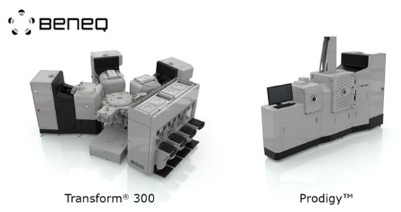
SEMI spoke with Dr. Patrick Rabinzohn, Strategic Development Executive of Semiconductor ALD at Beneq, about the benefits of ALD and shared how Beneq is building a comprehensive ALD product portfolio – from Beneq Transform® to ProdigyTM – covering different device applications and wafer sizes. We also talked about Beneq solutions to customer challenges, thanks to its vision and future trends for MtM devices for ALD.

SEMI: Beneq is already a familiar name in the ALD equipment business. For those new to the brand, please introduce the company.

Rabinzohn: Beneq is the home of atomic layer deposition and has ALD in its DNA. In fact, the very first industrial application of ALD was done in 1984 here on electroluminescent displays – the same location where Beneq still is headquartered today! Beneq was formed in 1984 and today we are a leading provider of ALD solutions for More-than-Moore semiconductor device fabrication with the Beneq Transform®.

Beneq’s state of art applications lab enables proof-of-concept and customer adoption for new ALD processes. Our team of engineers and experts is dedicated to making ALD tools accessible to our customers and partners.

SEMI: Beneq introduced the first Beneq Transform® in late 2019. How has adoption been so far?

Rabinzohn: The Beneq Transform® has revolutionized ALD cluster tools for More-than-Moore semiconductor markets in the EU, the U.S. and Asia since its launch in 2019. As of November 2021, Beneq has seen higher than expected demand for both the Transform and Transform Lite product configurations across key customer regions such as Europe, Japan, China, Taiwan and the U.S. We are super excited to see more customers adopting ALD in their More-than-Moore applications.