Showing posts with label NCD. Show all posts

Wednesday, January 10, 2024

NCD supplied repeated ALD equipment for special protective coating

NCD Co., Ltd. has again supplied large-scale productive ALD equipment to a Korean customer. It is for special coating parts used in semiconductor equipment to protect from corrosion and plasma arcing. This contracted equipment is the improved Lucida GSH Series ALD, which is capable of coating more and heavier products at once than the existing equipment. So the customer is able to obtain the greater increased productivity and reduced coating costs.

As semiconductor devices become smaller and more integrated, particles and byproducts that were not a problem before can significantly affect device performance, so the cleaning cycle and life time of parts used in semiconductor equipment are becoming shorter.


Lucida GSH Series ALD

Therefore, atomic layer deposition protective coating on parts can be a very effective solution, and high-quality, uniform atomic layer coating can achieve the effect of increasing the usage time of expensive parts in semiconductor equipment without cleaning and replacement.

Previously, atomic layer deposition protective coating was widely applied to expensive parts such as showerheads and ESCs, but recently, it has been applied to various semiconductor equipment parts with complex gas paths, quartz products with complicated shapes, and high-purity precursor canisters that require the lowest impurity control. The scope of application is gradually increasing so we will look forward to steady and continued expansion of products and markets in this application field.

This repeated contract confirms once again the excellence of NCD's industrial atomic layer deposition technology and equipment to its customers, and it showed NCD to have occupied the leader on the gradually expanding market of atomic layer deposition equipment for part protection coating. NCD will continue to pioneer new atomic layer deposition markets based on its best technology and customer trust.

Friday, November 4, 2022

Samsung use NCD ALD for wirebonding alternatives to expensive Gold

According to a recent article by TheElec, Samsung has developed a new chip packaging technology with its key partners for automotive chips. The company employs an aluminum oxide (Al2O3) coating bonding wire technology with improved reliability and insulation compared to previous bonding wires.

Bonding wires connect the I/Os with the lead frame or printed circuit boards. Most of them in the past have been made with gold (Au) as they are flexible and conductive. But as gold prices continue to rise, many companies attempt to mix them with silver (Ag) or copper (Cu). However,  these mixed materials usually have weak adhesiveness with their coating materials. This is unacceptable for chips aimed at automobiles as they are exposed to high-temperature and high-humidity environments.

Samsung’s aluminum alternative, which it is developing with Electron, NCD and LT Metal, doesn’t have this weakness since the aluminum oxide is coated at nanometer thinness onto the metal used as wire. Aluminum oxide bonds well with insulating coating materials that use epoxy. The precursors used to coat the aluminum oxide such as tri-metal aluminum (TMA) are also relatively cheap and used in HVM since a long time.


Insulated, Passivated & Adhesively-Promoted Bond WireUsing All-in-One Al2O3 Coating

Soojae Park(1), Jonghyun Lee(1), Chulhyung Cho(1), Namhoon Kim(1), Yongje Lee(1), Sichun Seo(1), Manho Kim(1), Youngkwon Yoon(1), EulgiMin(2), Kyujung Choi(2), Sang-Hoon Lee(3) Hong-Sik Nam(3),Monghyun Cho(4) & Jeongtak Moon(4),(1)Samsung Electronics Company130 Samsung-Ro, Yungtong-Gu, Suwon-Si, Gyunggi-Do, Republic of Korea(2)NCD Co., Ltd.(3)LT Metal, Ltd.(4)MK Electron Co., Ltd. (2) (PDF) Insulated, Passivated & Adhesively-Promoted Bond Wire Using All-in-One Al2O3 Coating. Available from:

Monday, October 10, 2022

NCD’s ALD technology and equipment for oxidation barrier of copper-based substrates

Copper is a metal used widely as the main material of Printed Circuit Board (PCB) and Lead Frame. But it is required to protect the oxidation because copper is easily oxidized in the condition of humidity, temperature, and pH, etc.

Electroless Nickel Immersion Gold (ENIG), Organic Solderability Preservative (OSP), Immersion Sn or Ag (ImSn or ImAg) is generally used to prevent oxidation of opened copper area after Solder Masking in PCBs. The lead Frame is protected from oxidizing by plating Au, Ag, Pd, and Ni after Lead Frame forming.

Recently, many groups have studied about preventing oxidation on the surface of copper by various corrosion protection layers of ALD metal oxides. Especially, Appling Al2O3 layer to the oxidation barrier is actively being researched.


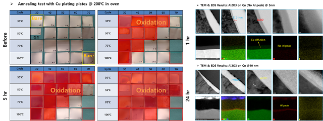
 < Surface images and TEM & EDS of Cu plates coated by ALD thin films after annealing test >

After depositing Al2O3 layers on Cu-plated plates with various film thicknesses and process temperatures, the oxidation and corrosion behavior of the coated copper was examined with different annealing times in the oven. There was no oxidation before annealing, but after annealing for 1hr, as the sample’s thickness lowered and process temperature decreased, the oxidation happened and increased gradually. There was no oxidation on the plates coated with 50~60 ALD cycles and at process temperatures of 70~100 after annealing for 5hr, and oxidation didn’t occur only in the case of 60 cycles and 100 after annealing for 24hr.

To analyze the change of the structure and confirm the oxidation behavior, TEM and EDS were measured on 5 and 10nm Al2O3 coated Cu plates at 100. The results showed that a thick Cu oxide layer was built by combining Cu coming out through the 5nm Al2O3 layer and outer oxygen after annealing.

On the other side, in the case of depositing 10nm Al2O3 film, the ALD layer was maintained after annealing, so Cu oxide layer wasn’t built on the surface. Therefore it confirmed that 10nm ALD Al2O3 layer showed an excellent corrosion barrier.


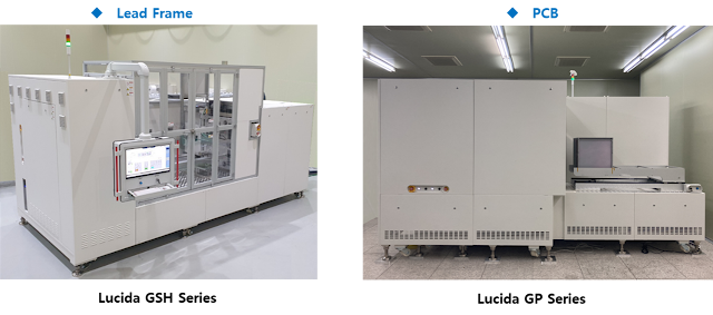
< ALD equipment for Lead Frame and PCB >

Copper-based PCBs and Lead Frames for semiconductors may have great properties to prevent humidity and oxygen by ALD-coated corrosion barriers.    

NCD has high volume and large area ALD equipment and technology for this kind of application. ALD tools for Lead Frames could be used by adding a dedicated transfer module on the base of Lucida GSH Series. And NCD has been developing new ALD equipment, Lucida GP Series, for large and flexible PCB substrates. NCD would extend the new ALD application area continuously through constant R&D.

Source: http://www.ncdtech.co.kr/2018/bbs/board.php?bo_table=eng_board_05&wr_id=57


Monday, September 26, 2022

Wafer scale microwire (TMW) solar cell with 21.1% efficiency using NCD ALD tool (Lucida D200)

[PV Magazine] Korean scientists have built a wafer-scale radial junction solar cell with tapered microwires and a surface passivation layer made of aluminum oxide. The device showed the highest power conversion efficiency among the previously reported microwire solar cells.


Crystalline silicon TMW solar cells are considered a potential alternative to conventional solar cells as these devices require thinner silicon wafers instead of the industry standard 160 µm thick wafers. “This could reduce manufacturing capital expenditure by 48% and module cost by 28%,” the Korean group claims.


Crystalline silicon TMW solar cells are considered a potential alternative to conventional solar cells as they require thinner silicon wafers instead of the industry standard 160 µm thick wafers. Image: Kangwon National University


A 10 nm-thick Al2O3 passivation layer was deposited on the front side of the wafer using ALD (Lucida D200, NCD) as reported in the publication below.

Choi, D., Hwang, I., Lee, Y., Lee, M., Um, H. D., & Seo, K. (2022). Wafer‐Scale Radial Junction Solar Cells with 21.1% Efficiency Using c‐Si Microwires. Advanced Functional Materials, 2208377.

Sunday, August 14, 2022

ALD IGZO application for Monolithic 3D Integration

Improvement of device performance and decrease of power consumption by scaling down in the semiconductor industry have almost reached the physical limit. Additionally, the possibility of memory’s capacitor collapsing has been increasing due to capacitors becoming narrower and higher so it can lead to reduced device reliability.

To escape the limit of scaling down, Monolithic 3D (M3D) technology which stacks layer by layer third dimension integration, would be available instead of planar scaling. Because it is scalable, performable, and economic, lots of companies, institutes, and universities are actively developing for its commercialization.

There is a limitation of upper layer process temperature because dopant diffusion, property degradation, and dimensional change in the lower device can happen during M3D integration. Therefore, to prevent the lower device from deteriorating, the process temperature for upper channel materials must be limited to not more than 450℃. IGZO has great properties and can be processed at low temperature so applying IZGO to M3D devices has been studied and developed, such as IGZO OSFET stacking on CMOS devices or RRAMs.


< Diagram of Monolithic 3D IC & Lucida™ S300 ALD >

Recently, IGZO is being applied to capacitor-less DRAM (2T0C) because IGZO TFT has very low off current (Ioff) by long retention time.

ALD IGZO enables conformal deposition and excellent thickness controllability. Also, composition control by cycle number ratio is accurate, so the bilayer structure can be easily deposited. It is expected to be applied for superb M3D devices.

NCD has been developing IGZO batch IGZO-ALD system with its creative technology, and it shows excellent film properties and high throughput with large area processing. LucidaTM S Series is available for developing M3D integration of Logic, Memory and electro-optics, etc.

LucidaTM S Series for semiconductor is a high throughput ALD system with thermal or plasma process for 300 mm wafers and is able to deposit various oxides (HfO2, ZrO2) and metals (TiN, TaN, Ru) with excellent property and film uniformity.

Source: www.ncdtech.co.kr

Wednesday, June 22, 2022

NCD supplied ALE and ASD equipment to Samsung Electronics Co., Ltd.

NCD has recently supplied ASD (Area Selective Deposition) equipment to Samsung Electronics Co., Ltd. Following ALE (Atomic Layer Etching).

This is the cluster system which consists of two process modules (PMs) and a wafer transfer module (TM) and applies a running program for process integration. In addition, it is equipped to process at high temperatures up to 500℃ and process with ozone and plasma for developing the next semiconductor devices.

ALE is able to etch a deposited layer by atomic scale as opposed to ALD and ASD can only deposit on the selective area not grow the whole area of substrates by ALD.

Today, lots of universities, institutes, and companies have actively been developing future high-tech and highly integrated devices using ALE and ASD processes.

NCD expects that the ALE/ASD system will contribute very much to the development of high-end semiconductor technology and is going to do all of the efforts to the best ALD equipment company with new challenges and continuous R&D.

<Lucida M200PL Series ALD System>


Monday, May 2, 2022

NCD supplied additional ALD equipment for special protective coating

Recently NCD supplied additional ALD equipment to the customer based in Korea. It is for coating products used in semiconductor equipment to protect from corrosion and plasma arcing.

This re-contracted equipment is Lucida GSH Series ALD. It is a fast and efficient ALD protective layer coating system with lower precursor usage than existing equipment. The customer is looking forward to extending the lifetime of high cost products through uniform and high quality ALD coating.

This repeat ordered supply shows that the customer has had confidence in the NCD’s ALD technology and the excellence of the equipment.


<LucidaTM GSH Series ALD>

Tuesday, November 9, 2021

NCD Supplied new ALD equipment for protective coating of semiconductor equipment’s products

NCD supplied new ALD equipment to the customer based in Korea for coating products used in semiconductor equipment to protect from corrosion and plasma arcing. The customer could expect longer part lifetime and lower operation expense through this special coating because of improving reliability of process and protecting parts from damages.

Productivity and cost competitiveness have been more and more important in semiconductor industry. Using special coating, the competitiveness could be much increased by protecting particle generation and damage of semiconductor production, and cost down by longer maintenance period.

Normally protective coating on parts is used thermal spray coating, anodizing process and sputtering but they have some limitation because it is difficult to coat uniformly on complicated and micro-shaped products by those methods. However ALD process could solve that problem.

Complex shaped shower heads and electro static chucks in the equipment using etching and dry cleaning process with corrosive gases as well as plasma, could be expected to apply ALD process. Because shower heads have a lot of fine holes and ESCs have wafer lift pin holes so those products couldn’t be coated uniformly by CVD and PVD methods. Therefore ALD might be very essential for special coating for these products.

ALD Al2O3 coating to protect part damage is used normally because Al2O3 process has already been confirmed in many application area. ALD Y2O3 will be studied actively for the next protective coating because it has much more anticorrosive property than ALD Al2O3.

This supplied equipment, Lucida GSH500, applied NCD’s creative high throughput and large area ALD technology could load multi semiconductor products at the same time and run uniform ALD coating. NCD will keep our best to develop the more competitive ALD technology and equipment to expand various new application fields in the future.


<Lucida GSH500>


Friday, July 2, 2021

Future foldable and flexible Display with NCD’s ALD encapsulation technology

In the global market of smart phones, competition on mobile’s form factors has been an important issue since foldable smart phones had launched following cured ones. Samsung electronics applied in-folding form factor to Galaxy Fold and Galaxy Z Flip, and Huawei used out-folding form factor to Mate X. New two or three folding form factor has been unveiling to the public beyond in-folding and out folding displays.

Flexible displays consist of Thin Film Transistor (TFT), Organic Light Emission Diode (OLED) and multi encapsulation layers. Generally organic and inorganic laminated layers is used for foldable displays and PECVD has applied to deposit inorganic materials.

Basically, Inorganic layers is lack of brittleness then their encapsulation property is degraded with continuous mechanical stress. ALD method for TFE was considered instead of PECVD due to their excellent encapsulation characteristics with thicknesses of few tens of nanometers. The reliability of the tool blocked applying to production at that time.

But because of the superior encapsulation property using ALD, many universities, institutes as well as display companies have been developing ALD inorganic layers for flexible displays and evaluating hundreds of thousand times folding test considering actual use recently.

LucidaTM GD Series ALD


The customer which has NCD’s Lucida GD Series ALD, measured folding test on flexible displays with inorganic layers using ALD instead of using PECVD and showed great performance under actual display operation. The 5.85 inch AMOLED display panels for in-folding and out-folding consisted of encapsulation structure of 30nm Al2O3 ALD/ 8㎛-Polymer/ 30nm Al2O3 and was tested in-folding and out-folding evaluation of 200,000 times with bending radius of 2R under light status after the 1st reliability test of RA 60℃/90% for 500hr. There were no dark spots on the panels after finishing the folding measurement. The 2nd reliability test of RA 60℃/90% for 48hr followed folding evaluation and then the TFE status was examined without any cracks.


Using NCD’s large area batch ALD system for foldable phones could obtain superior encapsulation property and flexibility with very thin inorganic layers to current ones using PECVD as well as provide great productivity because the batch tool can process lots of panels at one time.

Then NCD really looks forward to applying its large area batch ALD technology to encapsulation of future flexible display with in/out-folding and very small bending radius because of having solved the previous issues without both reliability and productivity that the reason is why ALD equipment didn’t apply for mass production of flexible display.

Friday, June 5, 2020

Thermal ALD IGZO Properties for LTPO TFTs by NCD

 
LTPS TFTs have been applied to most of the display for smart phones which consume most of the power for their operating because they have high electron mobility showing fast response time even if they have higher power consumption than that of IGZO TFTs,

Recently applications of LTPO (Low Temperature Polycrystalline Oxide) TFTs have been increasing to save the powder consumption of mobile and wearable devices. LTPO TFTs are the device combining LTPS TFTs with fast speed and Oxide TFTs with low leakage current. That is, switching uses Oxide TFTs because of being on/off the light fast and operating uses LTPS TFTs due to changing display rapidly with control of the mount of light.

A lot of smart device manufacturers including Apple are using or will use LTPO displays for their latest smart watches because their power consumption can decrease ~40%. Also, many manufacturers like Samsung and Apple have actively been developing their high-end smart phones equipped with the LTPO displays to make the power usage optimized.


General LTPO Structure and Properties

IGZO thin films used for Oxide TFTs have typically been processed by sputtering, but this method continuously has been showing lots of issues such as their bad thickness and composition uniformity, degradation of the physical and electrical properties due to plasma damage and the stability problem of targets. However using thermal ALD-IGZO, it is possible to deposit high quality thin films because of no plasma damage in process, low process temperature, and atomic scale controllability of thickness and composition.


Thermal ALD IGZO Properties

It is possible to get exact target atomic compositions of IGZO thin films by controlling the ratios of ALD cycle of respective sources in thermal ALD. Therefore this method could show the superior device properties to that by sputtering because it enables to control easily and exactly the most suitable atomic composition for the respective device structure of customers.

NCD has been developing high throughput batch IGZO-ALD system with its creative technology enabled to adapt the target atomic composition for respective devices. NCD could provide the competitiveness of excellent quality and the high productivity for LTPO TFTs including IGZO thin films using Lucida GD Series ALD which could process many and large area substrates at once.


NCD’s LucidaTM GD Series ALD

Source: http://www.ncdtech.co.kr/2018/bbs/board.php?bo_table=eng_board_05&wr_id=51

Thursday, March 26, 2020

NCD supplied two Lucida M300 ALD systems for R&D to KANC

NCD has recently supplied 2 Lucida M300PL ALD systems to KANC. Lucida M300PL-O is the equipment for oxide deposition with Ozone and Plasma process, and Lucida M300PL-M is that for metal deposition with Plasma process.

These wafer process equipment have the specification below

1) System: Lucida M300PL-O, Lucida M300PL-M

2) Substrate: Wafer 300mm

3) Deposition Materials:

- Lucida M300PL-O: Al2O3, TiO2, ZrO2, ZnO, HfO2, Ta2O5

- Lucida M300PL-M: Co. Ru, W, Ir, TiN, TaN

KANC, which is the most prestigious institute of Korea on nanotechnology, is using Lucida M300PL to investigate cutting edge semiconductor development and promising applications in MEMS and IoT. So it will be expected that these systems will contribute very much to the development of high-end nanotechnology.

NCD will do best to be the best ALD equipment company with continuous R&D efforts. 


< Lucida M300PL ALD >

Wednesday, January 15, 2020

Metal mask coating by ALD for reliable plasma process in PECVD

The PECVD method with metal masks has, in general, been used to deposit inorganic layers like SiNx and SiO2 for manufacturing LCD and OLED displays.

However, this plasma process has severe problems like plasma arcing or particle generation due to instability of electrical isolation between the metal mask and the showerhead as an RF electrode. Therefore it is required to deposit dielectric materials such as Al2O3, Y2O3, TiO2, MgO, ZrO2, etc. on the metal mask to prevent plasma damage.

Typically, the dielectric layer is coated by a sputtering method, also known as physical vapor deposition (PVD). However, this method is difficult to coat the metal mask uniformly with large area and complex structure as well as it has the disadvantage of requiring a thick deposition of several µm and multiple processes.

To obtain excellent electrical isolation properties of metal masks in the PECVD process, the atomic layer deposition (ALD) of Al2O3 thin film might be the best solution which enables getting uniform deposition on them with large area and complex structure. 

ALD Al2O3 layers could give them remarkable electric isolation and great protection, even if the thickness is less than one ㎛. When 50nm ~ 200nm layers of Al2O3 deposited by NCD large-area demo tool on metal masks were applied to the PECVD process, there was no issues like plasma arcing or damage. 

Images of metal mask coated by ALD with Al2O3 a) before (b) after

In fact, even though ALD Al2O3 has lots of advantages, the end customer has to consider of low throughput using general large-area ALD equipment. However, NCD’s Lucida GD Series for large-area ALD applications might be the most suitable equipment with superb productivity to provide superior protective layers to the metal masks from plasma issues in the PECVD process.

NCD has steadily developed large area and high throughput ALD equipment and technology. The applications for display, solar cell, and semiconductor fields have been already commercialized, and also NCD has worked hard to find use in special markets like excellent plasma protective coating on metal masks. NCD will aggressively respond to the development and then supply of ALD equipment, which customers would need for various industries in the future.


LucidaTM ALD system for metal mask coating.

Wednesday, November 13, 2019

Improvement of the quantum efficiency of micro LED by ALD passivation

Micro LED has been interested in the next generation display and been actively developing at many electronics manufactures and institutes for applications of AR/VR, wearable device and extra-large display as a core factor of the forth industry. Also it is evaluated to have superior properties to LED as well as OLED with low power consumption, excellent brightness, greater contrast, flexibility and reliability.

Micro LED of less than 10 µm size is required for displays needed high pixel per inch (PPI) but the quantum efficiency drop would occur by sidewall effect in the manufacturing process. Looking at the reason in detail, micro LED chips require separation of them by dry etching process and the sidewall effect reducing external and internal quantum efficiency happens not to optimize extraction of light by chemical contaminations and structural damages during the etching process.

ALD passivation on the sidewall of Micro LED after dry etching process

The passivation of sidewall by atomic layer deposition recover and remove the plasma damage by dry etching so that the quantum efficiency could be increased and also the ratio of improvement could increase as small as the size of micro LED.

Specially, the interest of productive ALD equipment has been gradually increased because of the excellent dielectric passivation by ALD Al2O3 thin films expecting to improve quantum efficiency.

NCD has been developing wafer based high throughput batch ALD system continuously enable to form high quality oxide passivation to improve the quantum efficiency of micro LED. By introduction of the system in production of micro LED, it could be expected to guarantee the productivity, high quality and performance reliability of high resolution micro LEDs for applications of AR/VR, flexible and wearable devices and extra-large displays.  

NCD Si wafer based batch ALD cluster system