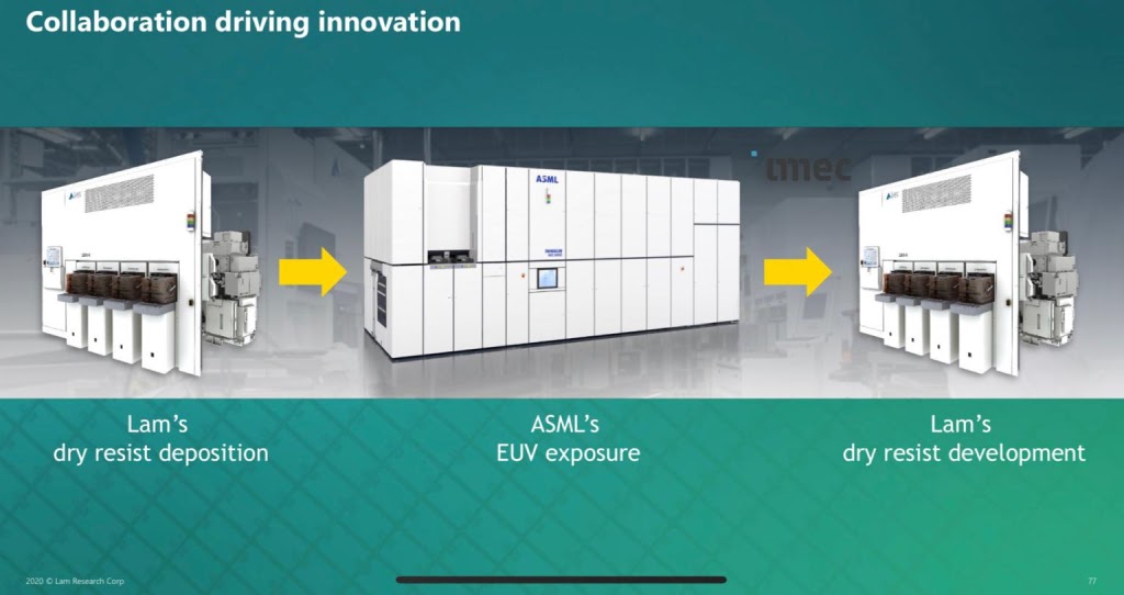
Sunday, July 17, 2022

Chipmetrics High Aspect Ratio Test Chip launched at ALD2022 in Ghent

At the recent AVS ALD2022 Conference in Ghent, Belgium, I made several rounds in the ALD industrial exhibition and met up with Chipmetrics Oy from Finland. Chipmetrics produce test structures, chips, and wafer concepts for advanced materials and microelectronics manufacturing, many specifically for ALD. Their main product – PillarHall test chip – is developed for advanced thin film process conformality characterization to accelerate applications of conformal 3D thin films. The Pillar Hall test chip has a lateral, very high aspect ratio structure to determine conformality when developing new ALD hardware, processes, and precursors.


Chipmetrics at AVS ALD2022 in Ghent, Belgium (Lower photo: Zahra Ghaderi, Mikko Utriainen and James Song)

What caught my eye this time was their new vertical high aspect ratio test chip - VHAR1 silicon test chip which consists of an array of vertical high aspect ratio holes. The holes have a constant hole diameter of 1 μm, and a depth of 200 μm over the whole chip area 15 × 15 mm. The deposited film penetration depth profile can be measured by cross-sectioning as normally done with the vertical high aspect ratio test structures.

This structure resembles the situation in semiconductor devices such as DRAM, 3DNAND, and TSVs. It can undoubtedly get valuable information and understanding when developing ALD processes for large surface areas with high aspect ratios. Anyone that has developed new ALD processes knows that not only the aspect ratio plays a role but also the total surface area since you need to achieve a sufficient dose of the precursors at the right process conditions to achieve perfect conformality very fast to be productive and minimize precursor decomposition, "CVD effects" and have effective purging of precursors and ALD process byproducts.

For more information, please find contact information here to Chipmetrics: LINK


Links

PillarHall – introduction in SlideShare

PillarHall – introduction in YouTube

PillarHall – short introduction in YouTube

Video: How to use PillarHall test chip

PillarHall Web Site

About Chipmetrics:

Chipmetrics is a forerunner in productizing test structures, test chips, and wafer concepts for advanced materials and microelectronics manufacturing.

We are experts in thin film conformality characterization. Our main product – PillarHall test chip – is developed for advanced thin film process conformality characterization to accelerate applications of conformal 3D thin films.

Chipmetrics Oy is a part of the emerging Atomic Layer Deposition (ALD) industry and research community. Our headquarters are in Finland – in the country of the origin of ALD.


Friday, July 15, 2022

Global Total Semiconductor Equipment Sales On Track to Record $118 Billion in 2022

SAN FRANCISCO, July 12, 2022 /PRNewswire/ -- Global sales of total semiconductor manufacturing equipment by original equipment manufacturers are forecast to reach a record $117.5 billion in 2022, rising 14.7% from the previous industry high of $102.5 billion in 2021, and increase to $120.8 billion in 2023, SEMI announced today in releasing its Mid-Year Total Semiconductor Equipment Forecast – OEM Perspective at SEMICON West 2022 Hybrid.

The following results reflect market size by segment and application in billions of U.S. dollars:


Both the front-end and back-end semiconductor equipment segments are contributing to the market expansion. The wafer fab equipment segment, which includes wafer processing, fab facilities, and mask/reticle equipment, is projected to expand 15.4% to a new industry record of $101 billion in 2022, followed by a 3.2% increase to $104.3 billion in 2023.

"In line with the semiconductor industry's determined push to increase and upgrade capacity, the wafer fab equipment segment is poised to reach the $100 billion milestone for the first time in 2022," said Ajit Manocha, president and CEO of SEMI. "Secular trends across a diverse range of markets, coupled with strong investments in digital infrastructure, are powering another record year."

Driven by demand for both leading-edge and mature process nodes, the foundry and logic segments are expected to increase 20.6% year-over-year to $55.2 billion in 2022 and another 7.9%, to $59.5 billion, in 2023. The two segments account for more than half of total wafer fab equipment sales.

Strong demand for memory and storage continues to contribute to DRAM and NAND equipment spending this year. The DRAM equipment segment is leading the expansion in 2022 with expected growth of 8% to $17.1 billion. The NAND equipment market is projected to grow 6.8% to $21.1 billion this year. DRAM and NAND equipment expenditures are expected to slip 7.7% and 2.4%, respectively, in 2023.

After surging 86.5% in 2021, the assembly and packaging equipment segment is expected to grow 8.2% to $7.8 billion in 2022 and edge down 0.5% to $7.7 billion in 2023. The semiconductor test equipment market is forecast to grow 12.1% to $8.8 billion in 2022 and another 0.4% in 2023 on demand for high-performance computing (HPC) applications.

Regionally, Taiwan, China, and Korea are projected to remain the top three equipment buyers in 2022. Taiwan is expected to regain the top position in 2022 and 2023, followed by China and Korea. Equipment spending for other regions tracked, except for Rest of World (ROW), is expected to grow in 2022 and 2023.

Source: SEMI July 2022, Equipment Market Data Subscription


ASM International launches TENZA ALD Quad Chambers for silicon oxide gap-fill and liners on the XP8 platform

New process technology addresses 300mm advanced memory and logic/foundry applications with best film quality, highest productivity and lowest cost of ownership in its class.

San Francisco, USA – ASM International N.V. (Euronext Amsterdam: ASM) today announced TENZATM ALD, an innovative single wafer atomic layer deposition (ALD) process technology for 300mm wafers. TENZATM ALD is optimized for gap-fill applications and provides the best film quality, conformal coverage through the full trench and highest productivity in its class.

Quad chamber modules (QCMs) 30, 32, 34, and 36 are connected to four side surfaces of the vacuum chamber 22. Each QCM is a module having four reactor chambers (RC1 to RC4). Processing such as plasma film forming processing is performed on a substrate in each reactor chamber. (ASM Patent application US20170278074A1) LINK: BALD Engineering - Born in Finland, Born to ALD: ASM International enhances ALD productivity with new 300 mm XP8 Quad Chamber Module

TENZATM ALD is offered on ASM’s high productivity quad chamber module (QCM) architecture, with four tightly integrated reactors on each QCM. In a compact configuration, up to 4 QCMs running the TENZATM ALD process can be attached to the XP8 platform, enabling processing of up to 16 wafers at a time.

“TENZATM ALD leverages ASM’s production proven QCM quad chamber module architecture and XP8® platform, which have been in high volume manufacturing fabs for several years, to bring enhanced process capability at the lowest cost of ownership to the market. TENZATM ALD enables ultra-high aspect ratio (>100:1) gap-fill for advanced memory devices”, said Hichem M’Saad, Chief Technology Officer and Member of the Management Board.

TENZATM ALD utilizes a novel design optimized for ALD reactions, minimizing process volume for maximum precursor utilization efficiency, reducing precursor consumption up to 50% and increasing productivity more than double compared to conventional ALD approaches. Each reactor chamber controls the RF plasma power supply and matching system individually to improve process reproducibility. The small volume reactor also provides excellent defect performance and extended reactor life (run time before preventive maintenance). Process reactions are confined within each small volume reactor space to minimize consumable parts, making maintenance very easy and less costly.

TENZATM ALD enables a variety of silicon oxide applications for gap-fill and liners for a range of structures in advanced transistors, memory devices and interconnects. The industry can count on TENZATM ALD to deliver a high quality, reliable, repeatable, production proven gap-fill process with the lowest cost of ownership on the market today.

Deliveries of TENZATM ALD have begun to multiple global customers, among them leaders in memory device manufacturing. ASM’s mature compact ALD quad chamber module architecture has a proven track record with more than 2,000 reactors shipped to customers.

Thursday, July 14, 2022

Lam Research, Entegris, Gelest Team Up to Advance EUV Dry Resist Technology Ecosystem

Collaboration provides robust chemical supply chain for global chipmakers using the breakthrough technology and supports R&D for next-generation EUV applications


SEMICON WEST 2022, SAN FRANCISCO, July 12, 2022 – Lam Research Corp. (NASDAQ: LRCX), Entegris, Inc. (NASDAQ: ENTG), and Gelest, Inc, a Mitsubishi Chemical Group company, today announced a strategic collaboration that will provide semiconductor manufacturers worldwide with reliable access to precursor chemicals for Lam’s breakthrough dry photoresist technology for extreme ultraviolet (EUV) lithography, an innovative approach used in the production of next-generation semiconductors. The parties will work together on EUV dry resist technology research and development (R&D) for future device generations of logic and DRAM products that will help enable everything from machine learning and artificial intelligence to mobile devices.


A robust supply chain for process chemicals is critical to EUV dry resist technology integration into high-volume manufacturing. This new long-term collaboration further broadens the growing ecosystem for dry resist technology and will provide dual-source supply from semiconductor material leaders with provisions for continuity of delivery in all global markets.


LAM is a semiconductor processing and fabrication equipment designer and manufacturer who has announced a new dry photoresist technology in collaboration with IMEC and ASML. This new dry technology differs from the wet photoresist currently used in all commercial semiconductor foundries such as TSMC, Intel, Samsung, Micron, Global Foundries and SK Hynix. (source: SemiAnalysis LINK)


These stochastic defects lead to a variety of issues with the future 3nm/2nm nodes. One of these issues that can be mitigated by moving to dry deposit and develop is line collapse. When the solvent is washed away, the lines can become unstable and collapse. Other issues such as line edge roughness are also mitigated when moving to a dry deposit and develop flow. (source: SemiAnalysis LINK)

In addition, Lam, Entegris, and Gelest will work together to accelerate the development of future cost-effective EUV dry resist solutions for high numerical aperture (high-NA) EUV patterning. High-NA EUV is widely seen as the patterning technology that will be required for continued device scaling and advancement of semiconductor technology over the coming decades. Dry resist provides the high etch resistance and tunable thickness scaling of deposition and development necessary to support high-NA EUV's reduced depth of focus requirements. "Dry resist technology is a breakthrough that shatters the biggest barriers to scaling to future DRAM nodes and logic with EUV lithography," said Rick Gottscho, executive vice president and chief technology officer of Lam Research. "This collaboration brings together Lam's dry resist expertise and cutting-edge solutions with material science capabilities and trusted supply channels from two industry precursor chemical leaders. This important expansion of the dry resist ecosystem paves the way for exciting new levels of innovation and high-volume manufacturing with the technology." First developed by Lam in collaboration with ASML and IMEC, dry resist extends the resolution, productivity, and yield of EUV lithography, thereby addressing key challenges associated with creation of next-generation DRAM and logic technologies. It provides superior dose-to-size and dose-todefectivity performance, enabling higher EUV scanner productivity and lower cost of ownership. In addition, Lam's dry resist process offers key sustainability benefits by consuming less energy and five to ten times less raw materials than traditional resist processes. "Lam's dry resist approach reflects key innovations at the material level and offers a wide range of advantages, including better resolution, improved cost-efficiency and compelling sustainability benefits," said Bertrand Loy, chief executive officer of Entegris. "We are proud to be a part of this innovative collaboration to accelerate dry resist adoption and to be a trusted process materials supplier for customers as they push to create the next generation of semiconductors with this important technology." "Our collaboration with Lam and Entegris to advance dry resists for EUV lithography demonstrates our commitment to support chipmakers as they innovate in materials science," said Jonathan Goff, president of Gelest, a Mitsubishi Chemical Group company. "We've seen EUV demonstrate exceptional value in recent years, and we're pleased to be part of the growing ecosystem to extend its potential."

Tuesday, July 12, 2022

ASM Internaltional launces new 300 mm Vertical batch for LPCVD and ALD

New system addresses 300mm advanced logic/foundry and memory applications with highest productivity and lowest cost of ownership in its class

San Francisco, USA – ASM International N.V. (Euronext Amsterdam: ASM) today introduced the SONORA® vertical furnace system with dual reactor chambers for 300mm wafers. The system’s dual boat reactors produce the highest available throughput in its class, increasing reactor utilization to virtually 100%, while ensuring the lowest capex.


SONORA is named after the blossoming Sonoran desert near Phoenix, Arizona. The look and feel of the SONORA system reflects the colors of the Saturn rockets from the Space Age - a time when semiconductor technology was given a huge boost. It is also the era that gave birth to ASM, and so the SONORA® color scheme creates a link to ASM’s more than 50-year legacy in semiconductor processing equipment. LINK: SONORA_vertical_furnace (asm.com)

“The introduction of the novel SONORA® system is part of our strategy to selectively grow our vertical furnace presence in the market. The new SONORA® ensures that ASM will be strengthening its offering in advanced logic/foundry and memory applications as well as extend our leadership position in the market for More than Moore (such as analog and power) applications,” said Hichem M’Saad, Chief Technology Officer and Member of the Management Board.

The new SONORA® is fully compatible with the original A412™, so existing process recipes are easily transferred, accelerating system qualification and ramp up. System deliveries have begun to multiple customers globally, among them leaders in advanced logic, and power device manufacturing.

ASM’s predecessor A412™ vertical furnace system has a proven track record of more than 1,000 reactors shipped to customers worldwide and over 22 years of maturity in semiconductor manufacturing. The new SONORA® has a novel system architecture that maximizes floor space productivity as well as service area. Its dedicated process modules have individually controlled high purity mini environments. Our innovative gas injection system for low pressure processing provides the best uniformities of deposited films between the individual wafers at larger load sizes. These larger process wafer load sizes combined with the updated control system, new robots, faster wafer cooldown, faster boat exchange modules generate up to 30% more productivity, compared to its predecessor. Higher productivity also results in lower energy and chemical usage per wafer. Special attention was given to the design for serviceability leading to a spacious access for all maintenance activities. The new system has been further modernized with an intuitive graphical user interface, predictive maintenance by advanced control diagnostics, and plug & play installation. Customers can count on the SONORA® delivering increased reliability and better ease of use with production output that achieves better repeatability, productivity, and time utilization.


The A412 PLUS is for 300mm wafers, while the A400 is for 200mm and smaller wafers sizes

Like its predecessor, the SONORA® offers a comprehensive portfolio of process applications including low pressure chemical vapor deposition (LPCVD) processes like doped silicon and silicon nitride films, diffusion processes such as wet oxidation and anneal processes, as well as a leading portfolio of atomic layer deposition (ALD) materials.

Supply chain limited by Russia / US CHIPS Act a game changer

San Diego, CA, July 6, 2022: TECHCET—the electronic materials advisory firm providing business and technology information— is forecasting semiconductor manufacturing materials to top US$65 B for 2022, a healthy 8% above 2021. “Semiconductor demand has remained strong through the first part of the year and average selling prices for materials are trending upwards,” cited Lita Shon-Roy, TECHCET’s President/CEO. In anticipation of slower market conditions, semiconductor materials market growth is currently forecasted to increase just over 2% in 2023 before further improving in 2024. “This is in keeping with cycles in demand and inventory volumes,” said Shon-Roy, as “per the latest TECHCET Critical Materials Reports™,” shown in the figure below.


While demand remains strong in 2022, a number of issues are impacting materials supply and pricing. The Russia/Ukraine region is a major part of the oil and natural gas supply chain, of which energy, specialty gases and helium are dependent. It was a region expected to play a significant role in the supply of helium this year, in addition to supporting neon and fluorocarbon production used for semiconductor manufacturing. Due to the turmoil in this area, alongside related economic sanctions against Russia, supply of these and other key gases have been curtailed, straining supply-chains around the world. Additionally, energy costs have steeply risen creating cost escalation of materials production worldwide.

Monday, July 11, 2022

AlixLabs at AVS ALD ALE 2022 in Ghent, Belgium

AlixLabs AB participated and presented at The AVS 22nd International Conference on Atomic Layer Deposition (ALD 2022) featuring the 9th International Atomic Layer Etching Workshop (ALE 2022) in Ghent, Belgium June 27 to 29.

Yoana gave her oral presentation in session LE1-TuA-4 In-situ Optical Emission Spectroscopy as a Tool to Characterize Cyclic Quasi-Atomic Layer Etching, Yoana Ilarionova, Lund University, Sweden; M. Karimi, AlixLabs, Sweden; D. Lishan, D. Geerpuram, Plasma-Therm LLC, USA; R. Jafari Jam, D. Suyatin, J. Sundqvist, AlixLabs, Sweden; I. Maximov, Lund University, Sweden

Jonas gave an invited talk for TECHCET LLC CA in: AA2-TuM2-1 High ALD Equipment and Precursor Demand and 5-Year Forecast Due to Continued Semiconductor Device Scaling and Fab Expansions.

Dmitry as part of the AVS ALE Scientific Committee moderated the session ALE1-TuA In situ Studies, Mechanisms, and Modeling of ALE. We had a fantastic time and met a lot of old friends and made new ones!


Team photo: Reza Jafari Jam, Jonas Sundqvist, Yoana Ilarionova and Dmitry Suyatin.


Reza and Yoana taking on the ALD / ALE industrial exhibition.


Ghent by night, view from the Beneq party in the main castle - Gravensteen.


Dinner in a Castle.

Boat trip in beautiful Ghent


New slim line of MFCs and Valves from Fujikin.


Dmitry and Jonas met up with AlixLabs' long-time supporters Prof. Fred Roozeboom and Dr. Jacques Kools.


Yoana getting questions from Prof. Steven .M. Geroge himself.


Yoanas title slide.


ALE - the icing on the cake


Angélique Raley from Tokyo Electron USA giving the best ALE talk!


AlixLabs sponsored the Social Media Chair 2022 - please check Twitter by the Social Media Chairs @Mick__geek and @hacp81
 for more famous ALD and ALE people 


AVS ALD ALE 2022 Page: ald2022.avs.org/

New world records: perovskite-on-silicon-tandem solar cells

EPFL and CSEM smash through the 30% efficiency barrier for perovskite-on-silicon-tandem solar cells —setting two certified world records 

Neuchâtel, July 7, 2022 – For the first time, an efficiency of 30% for perovskite-on-silicon-tandem solar cells has been exceeded thanks to a joint effort led by scientists at EPFL’s Photovoltaics and Thin Film Electronics Laboratory in partnership with the renowned innovation center, CSEM. Independently certified by the National Renewable Energy Laboratory (NREL) in the United States, these results are a boost to high-efficiency photovoltaics (PV) and pave the way toward even more competitive solar electricity generation.


Left and right panels: Schematics of perovskite-on-silicon tandems that are either flat or textured on their front side. Upper central panels: scanning electron microscopy images of the two types of devices developed by EPFL and CSEM. Lower central panels: corresponding picture. Credit: D. Türkay (EPFL), C. Wolff (EPFL), F. Sahli (CSEM), Q. Jeangros (CSEM).

More information: LINK

By Abhishekkumar Thakur