Showing posts with label Solar. Show all posts

Wednesday, December 27, 2023

Exploring Ultrathin Solar Cells with Professor Carl Hägglund: A Journey from Stanford's ALD Techniques to Plasmonic Solar Cell Optimization

In this episode, Tyler is joined by Professor Carl Hägglund from Uppsala University. They discuss Carl’s motivations for pursuing ultrathin solar cells, how he learned ALD at Stanford in Stacey Bent’s lab, and an unlikely research connection through his child’s school. They also talk about why ALD is useful for plasmonic solar cells, optimization of SnS ALD and his planned path towards a fully realized ultrathin photovoltaic.


00:00 Introduction
01:45 Motivation for fabricating plasmonic solar cells
09:58 Learning ALD at Stanford
22:46 Optimizing SnS ALD process
30:33 Path towards an ultrathin solar cell

Wednesday, November 1, 2023

KTH and Green14 Innovates Green Silicon Production to Challenge Asia's Dominance in Solar Cell Market

The traditional methods dependent on fossil fuels to reduce silicon dioxide are being challenged by KTH and Green14's reactor, which has a fossil-free process using hydrogen-based plasma reduction. This high-temperature plasma, created from a combination of hydrogen and argon gas, emits water vapor instead of carbon dioxide and has silane as another byproduct, used for producing silicon anodes for lithium-ion batteries.

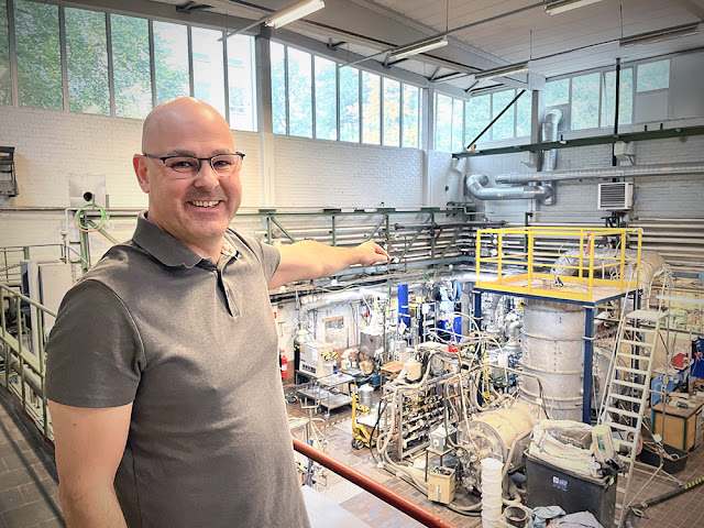
KTH (Royal Institute of Technology in Stockholm, Sweden) is challenging China's silicon production. A portrait depicts researcher Björn Glaser in a lab hall, pointing out the location where a reactor will be constructed. This seven-meter-tall reactor, being developed in collaboration with startup company Green14, aims to produce green silicon at KTH and challenge Asia's dominance in the solar cell silicon market.


Björn Glaser, researcher and project manager, points out the location in the so-called furnace hall where a reactor will be built. (Photo: Anna Gullers)

In a few months, the new reactor will begin construction at the Department of Materials Science, reaching the ceiling of the grand furnace hall, becoming KTH's largest pilot facility. The researchers aim to develop a process for silicon production that's faster and more environmentally friendly than previous methods.

Using 3,000-degree hydrogen plasma, the reactor will convert silicon dioxide to silicon, crucial for manufacturing solar cells and semiconductors. Unlike traditional methods that rely on fossil fuels, this process with hydrogen plasma emits water vapor instead of carbon dioxide.

The primary goal is to produce silicon suitable for solar cells, a market dominated by Asia, particularly China. Björn Glaser, a lecturer and expert in high-temperature metallurgical experiments, believes this could be a game-changer, potentially bringing Europe back into competition.

Green14, the startup behind the initiative, will own and operate the facility, with Björn Glaser and Adam Podgorski, an Australian chemist and CEO of Green14, working closely together. If successful, Green14 plans to build a larger facility in northern Sweden. However, a significant challenge is ensuring safety due to the combination of extremely high temperatures and hydrogen gas.

Björn Glaser expresses that the project not only provides good PR for KTH but also offers students a unique opportunity to engage in groundbreaking research. If successful, the process could revolutionize how other metals, like copper, titanium, and vanadium, are produced, reducing their carbon footprints and making them cheaper to manufacture.

About GREEN14

GREEN14 is a pioneering technology company committed to developing innovative solutions for a sustainable future. With a focus on renewable energy, GREEN14 is revolutionizing the production of solar grade silicon through its groundbreaking quartz reduction process. By combining cutting-edge technology with a commitment to environmental stewardship, GREEN14 is driving the transition to a low-carbon economy and paving the way for a cleaner, brighter future.

Sources:

KTH utmanar Kinas kiselproduktion | KTH

General 2 — Green14

Monday, October 16, 2023

US Researchers Achieve Record 25.1% Efficiency with Large Perovskite-Silicon Tandem Solar Cell

US scientists have achieved a breakthrough in photovoltaic (PV) cell technology by creating a large-area perovskite-silicon tandem solar cell measuring 24 cm2. This tandem cell has achieved a remarkable steady-state power conversion efficiency of 25.1%. To overcome common issues associated with scaling up perovskite solar technologies, such as shunting losses that create alternate pathways for solar-generated charge and lead to power losses, the researchers inserted a lithium fluoride (LiF) interlayer between a hole transport layer (HTL) and a wide bandgap (WBG) perovskite absorber. This interlayer improves physical contact and reduces shunting. The tandem cell demonstrated an efficiency of 25.2% under standard conditions, making it one of the most efficient two-terminal tandem devices for areas exceeding 10 cm2. This development holds promise for efficient, reproducible, and large-scale perovskite-silicon tandem solar cells.


Current-voltage curves for a perovskite mini-module with an aperture area of 42.9 cm2 Image: University of North Carolina at Chapel Hil, Cell Reports Physical Science, Creative Commons License CC BY 4.0

ALD is an important technology in perovskite solar cell fabrication. It enables precise, nanoscale control of layer thickness, ensuring uniform coverage even on complex surfaces. ALD is used for depositing passivation layers to reduce defects and enhance stability, creating protective barriers against environmental factors, engineering interfaces for improved charge transport, and ensuring compatibility with various materials. These applications contribute to improving the efficiency and long-term stability of perovskite solar cells, making ALD an essential tool in their development and optimization.

For deployment in solar cells, "perovskite" denotes a particular class of materials employed as the light-absorbing layer. These perovskite solar cells utilize a group of materials characterized by a crystalline structure akin to that of the mineral perovskite, named after Russian mineralogist Lev Perovski. Typically, these materials are comprised of organic-inorganic hybrid compounds, with common examples including methylammonium lead iodide (CH3NH3PbI3) and formamidinium lead iodide (HC(NH2)2PbI3). Perovskite solar cells have garnered substantial interest due to their potential for high efficiency, cost-effectiveness in production, and simplified manufacturing processes. Researchers are diligently working to enhance the efficiency, stability, and scalability of perovskite solar cells to position them as a competitive and sustainable renewable energy solution.

Sunday, September 24, 2023

Stockholm-Based GREEN14 Leads the Charge in Sustainable Silicon Production for Solar Industry

Stockholm-based GREEN14 is making strides in its mission to revolutionize solar-grade silicon production. Following a successful lab-scale feasibility study, the company is set to establish a pilot plant using a pioneering quartz reduction process with hydrogen plasma. Emissions are expected to decrease by 60% to 95%, aligning with the company's commitment to sustainability. The technoeconomic analysis suggests the pilot plant will be economically viable, potentially transforming the solar industry. The plant, scheduled to be commissioned at KTH, signifies GREEN14's dedication to academic collaboration and clean energy innovation. Founder Adam Podgorski anticipates a significant positive environmental impact.

Green 14 is pioneering a sustainable shift in silicon production methods, potentially revolutionizing the solar panel manufacturing industry. Their innovative approach, protected by a patented solution, seeks to redefine how silicon is extracted from quartz. Unlike the traditional reliance on coal, Green 14 utilizes green hydrogen, a cleaner energy source, to convert silicon dioxide into silicon. This transition significantly reduces energy consumption and replaces carbon dioxide emissions with water vapor, offering a more environmentally friendly alternative.


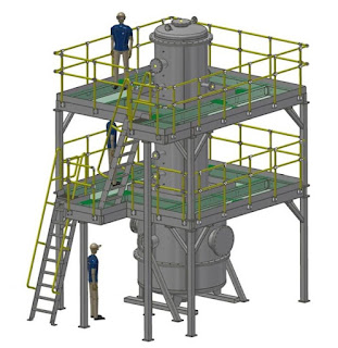
"This is what the initial design of a reactor producing the world's first kg/hour of green solar grade silicon looks like. When we succeed we will have silicon with up to 95 percent GHG reduction at a cost lower than the leading Chinese producers." Source Green14 LinkedIn.

Green 14's primary goal is to reduce the carbon footprint associated with solar panel production, addressing the inherent environmental challenges in the industry. In a world where fossil fuels dominate manufacturing processes, Green 14's commitment to eco-conscious innovation signifies a potential shift toward a greener future.

Their recent successful lab tests mark a promising step forward. However, their most significant project lies ahead—an ambitious eight-meter-high test reactor set to be constructed at the Department of Materials Science at KTH. This project aims to scale up production and transition from batch processing to a more efficient continuous manufacturing process. The ultimate objective is to produce high-purity silicon on a larger scale, potentially setting new industry standards.


While Green 14 maintains the confidentiality of their innovative technology, their use of hydrogen plasma as a reducing agent and operation at temperatures of 3,000 degrees Celsius underline their commitment to technological advancement. The hope is that this approach will not only prove cost-effective but also more energy-efficient and environmentally sustainable compared to prevalent manufacturing methods, which often rely heavily on fossil fuels and are largely concentrated in China.

The estimated cost of the pilot facility at 20 million Swedish kronor reflects Green 14's earnest endeavor to introduce this transformative technology. Pending grant approvals from the Swedish Energy Agency and Vinnova, Green 14 is poised to make a significant impact on the future of solar panel manufacturing. The pilot facility, expected to commence operations soon, signifies a pivotal step toward a more sustainable and cleaner energy future.

About GREEN14
GREEN14 is a pioneering technology company committed to developing innovative solutions for a sustainable future. With a focus on renewable energy, GREEN14 is revolutionizing the production of solar grade silicon through its groundbreaking quartz reduction process. By combining cutting-edge technology with a commitment to environmental stewardship, GREEN14 is driving the transition to a low-carbon economy and paving the way for a cleaner, brighter future.

Sunday, August 27, 2023

Dutch Scientists at TNO & TU Eindhoven Develop Efficient Monolithic Perovskite-PERC Tandem Solar Cell

Highlights

  • Champion 23.7% efficient perovskite-PERC tandem cell was achieved.

  • The developed thermal atomic layer deposition (ALD) process for NiO is reported.

  • ALD NiO was added to an ITO/SAM recombination junction to improve the device yield.

Dutch researchers at TNO and TU Eindhoven have achieved a notable breakthrough in solar cell technology by creating a monolithic perovskite-PERC tandem solar cell with a remarkable 23.7% efficiency. The innovation lies in a new tunnel recombination junction (TRJ) design that includes indium tin oxide (ITO), carbazole (2PACz), and a nickel(II) oxide (NiO) layer. Unlike conventional TRJs, the addition of NiO significantly reduces electrical issues in the perovskite top cell.


(a) HAADF-scanning transmission electron microscopy (TEM) image of a tandem cell using ITO/NiO/2PACz. (b) Compositional line profiles at the interface ITO/NiO/SAM extracted from an EDX elemental mapping. Note that the figure is rotated 90°.

By using atomic layer deposition (ALD), the team improved the uniformity of the self-assembled monolayer (SAM) in the TRJ structure. This new solar cell design includes a perovskite absorber, electron transport layers, an ITO electrode, a silver (Ag) metal contact, and an antireflective coating.

Comparing their creation with a reference cell, the researchers found the novel TRJ-based cell achieved an efficiency of 23.7%, slightly below the reference cell's 24.2%. However, the novel design's uniform coverage of SAM and consistent efficiency across different devices within and between batches makes it promising for large-scale production.

Published in Solar Energy Materials and Solar Cells, this research opens doors for improved perovskite-PERC tandem solar cell technology using ALD NiO.

Atomic layer deposition of NiO applied in a monolithic perovskite/PERC tandem cell - ScienceDirect

Monday, June 12, 2023

Black Ultra-Thin Crystalline Silicon Wafers Achieve Maximum Absorption Limit for Improved Solar Cell Efficiency

State-of-the-art black silicon nanotexture enables ultra-thin silicon photovoltaics with enhanced light trapping and improved performance.

Finnish and Spanish researchers have made a breakthrough in the development of ultra-thin crystalline silicon wafers for solar cells by reaching the maximum theoretical absorption limit using advanced black silicon nanotexture. The achievement not only addresses the challenge of maintaining high absorption in thin wafers but also offers significant cost reductions in the photovoltaic industry. The study demonstrates that wafer thicknesses as low as 10 µm can achieve ideal light trapping.


a) Measured absorption of thin silicon wafers (10, 20, and 40 µm nominal thickness) with polished surfaces (orange) and with black silicon texture etched on the front side (blue). Solid and dashed lines represent absorption with and without back a reflector, respectively. The dotted line corresponds to Yablonovitch's 4n2 absorption limit. b) Scanning electron microscope (SEM) image, bird's eye view, of the black silicon nanotexture obtained by DRIE. The scale bar represents 1 µm. c) A free-standing 10µm-thick black silicon wafer, where its high flexibility can be appreciated. d,e) Top view of two 10 µm wafers: d) textured with black silicon and e) out-of-the-box with polished surfaces.

Reducing wafer thickness is a key strategy for cutting costs in the crystalline silicon photovoltaic industry. Thinner wafers significantly reduce substrate-related expenses. However, the weak absorption of silicon at long wavelengths poses a challenge when reducing wafer thickness. To overcome this, the researchers employed black silicon nanotexture, generated through deep reactive ion etching (DRIE) at cryogenic temperatures. The nanotexture allows for better light management and extends the optical path through internal dispersion and scattering, thus improving photon absorption.

The study also includes the implementation of black silicon nanotexture in an interdigitated back-contacted (IBC) solar cell. The proof-of-concept cell, encapsulated in glass, achieved an impressive 16.4% efficiency, representing a 43% increase in output power compared to a reference polished cell. The results highlight the potential of black silicon nanotexture for future ultra-thin silicon photovoltaics, offering both economic savings and improved cell efficiency.

Conventional techniques like chemical texturization through random pyramids and advanced nanopatterning methods have limitations in terms of material consumption, surface damage, and cost. Black silicon nanotexture produced through cryogenic DRIE offers several advantages, including minimal silicon consumption, low surface recombination, and compatibility with high-efficiency IBC solar cell structures. The researchers successfully applied black silicon nanotexture to ultra-thin monocrystalline substrates, demonstrating its potential for mass-produced ultra-thin crystalline silicon photovoltaics.

This study contributes to the ongoing efforts to make solar energy more cost-effective and efficient. The use of black silicon nanotexture in ultra-thin silicon wafers opens up new possibilities for next-generation solar cell technologies, paving the way for widespread adoption of renewable energy solutions. 

Source: 

Black Ultra-Thin Crystalline Silicon Wafers Reach the 4n2 Absorption Limit–Application to IBC Solar Cells

First published: 31 May 2023
 

Black Ultra‐Thin Crystalline Silicon Wafers Reach the 4n2 Absorption Limit–Application to IBC Solar Cells - Garín - Small - Wiley Online Library

Friday, November 4, 2022

ALD coatings for next-generation solar cells

(Helsinki : LINK) Researchers at the University of Helsinki are developing thin films needed in new types of halide perovskite solar cells, and matching ALD processes, in order to provide increasingly affordable solar cells, enable their integration into objects and, consequently, promote the transition to renewable energy.

The 2022 Millennium Technology Prize has been awarded today October 25 to Scientia Professor Martin Green of the UNSW Sydney, Australia, for his innovation that has transformed the production of solar energy.


Members of the research group next to the ALD reactor. Georgi Popov (left), Marianna Kemell, Alexander Weiss and Mariia Terletskaia. (Image: Riitta-Leena Inki)

Most commercial solar cells are silicon-based, and apply PERC (Passivated Emitter and Rear Cell) technology originally launched in 1983 by Martin Green, a recently awarded Millennium Award. However, increasingly efficient, inexpensive and durable solar cells are being developed all over the world. Even in the case of silicon-based cells, a transition is underway to novel techniques, including the tunnel oxide passivated contacts (TOPCon) concept, where several layers of silicon and oxide are added to the cell.

Transparent and flexible solar cells
In addition to silicon, other solar cell technologies are being investigated. The most promising new technique is based on the use of halide perovskites as a light-absorbing material. The general chemical formula of halide perovskites is ABX₃, where A is an alkali metal or an amine, B is tin or lead, and X is a halide. The most commonly studied compound is methylammonium lead iodide CH₃NH₃PbI₃. Perovskite solar cells are on the verge of commercialisation, and some manufacturers believe they will be mainstream in a couple of decades.

“As these new types of solar cells can be transparent, they can be installed in, for example, windows. They are also flexible, which increases their uses,” says Senior University Lecturer Marianna Kemell, who heads the research project funded by the Academy of Finland.

Even though halide perovskite solar cells have achieved high efficiency levels, problems with cell stability and the lack of industrial-scale production techniques have constituted bottlenecks impeding their widespread adoption.

A breakthrough with metal iodides
While pursuing a master’s degree in chemistry, Doctoral Researcher Georgi Popov boldly chose halide perovskites and their atomic layer deposition (ALD) as the topic of his master’s thesis. There were doubters, as prior research-based knowledge was scarce.

“We identified suitable chemicals and were able to design a reaction that enabled us to create a metal iodide coating through deposition for the first time. We were able to demonstrate that this can actually be done through atomic layer deposition. The first successful trial was carried out with lead iodide, which was then processed into CCH₃NH₃PbI₃ perovskite through a further reaction,” Popov says. “The research article was published in the refereed Chemistry of Materials scholarly journal. Later on, we also developed ALD processes for caesium iodide and CsPbI₃ perovskite.”

Coatings produced through atomic layer deposition are used in roughly 30% of silicon-based solar panels. The ALD group headed by Professor Mikko Ritala at the University of Helsinki has achieved promising results in terms of the technique’s adaptability to perovskite solar cells. The advantage of coatings produced by atomic layer deposition is that they form a uniform and comprehensive layer even on rough surfaces.

“If at some point we start making tandem solar cells, which combine a silicon cell and a perovskite cell, we know how to make that perovskite. We are developing the recipes and the chemistry used to grow perovskite,” Popov says.

While the work currently being carried out is basic research, developing recipes and experimenting with small surface areas, the technique is applicable to large-scale production.

“The current plants manufacturing solar cells in China and elsewhere are able to adjust their equipment to produce ALD-coated solar cells,” says Popov.

The future of solar cells
More than 80% of solar cells are manufactured in China, where industrial-scale ALD devices are also produced. Wei-Min Li, PhD, an alum of the University of Helsinki’s Department of Chemistry, works as the chief technology officer at Leadmicro, a leading Chinese manufacturer of ALD equipment. This connection gives the department a solid grasp on where the field is going. ALD equipment used to produce silicon-based solar panels can also be expanded to produce next-generation solar cell materials.

“We are developing the future technical solutions that will gradually replace and supplement current production. In the future, fewer resources will be needed for production, and, thanks to increasingly effective cells, less surface area as well. When solar cells can be installed on uneven surfaces in addition to even ones, we no longer need to build solar parks in fields, as fields are needed for other purposes,” Popov notes.

However, Popov points out that we cannot afford to wait for new technical solutions, as the utilisation of renewable energy sources must be increased now. By replacing current sources of energy with solar or wind power as much as possible, pressure will increase and the entire field will advance.

“The best part of silicon-based cells is that they last roughly 20 to 30 years and will continue to function even after that, albeit possibly less efficiently. Since solar cells produced with the PERC technique are the current state of the art, and they are available, it is advisable to acquire as many of them as possible. They will pay for themselves,” Senior University Lecturer Kemell says.

The project entitled ‘Atomic Layer Deposition as key enabler of scalable and stable perovskite solar cells’, which is funded by the Academy of Finland, will continue until 2024. In addition to Marianna Kemell and Georgi Popov, contributing to the project are Doctoral Researcher Alexander Weiss and master’s student Mariia Terletskaia.

Monday, September 26, 2022

Wafer scale microwire (TMW) solar cell with 21.1% efficiency using NCD ALD tool (Lucida D200)

[PV Magazine] Korean scientists have built a wafer-scale radial junction solar cell with tapered microwires and a surface passivation layer made of aluminum oxide. The device showed the highest power conversion efficiency among the previously reported microwire solar cells.


Crystalline silicon TMW solar cells are considered a potential alternative to conventional solar cells as these devices require thinner silicon wafers instead of the industry standard 160 µm thick wafers. “This could reduce manufacturing capital expenditure by 48% and module cost by 28%,” the Korean group claims.


Crystalline silicon TMW solar cells are considered a potential alternative to conventional solar cells as they require thinner silicon wafers instead of the industry standard 160 µm thick wafers. Image: Kangwon National University


A 10 nm-thick Al2O3 passivation layer was deposited on the front side of the wafer using ALD (Lucida D200, NCD) as reported in the publication below.

Choi, D., Hwang, I., Lee, Y., Lee, M., Um, H. D., & Seo, K. (2022). Wafer‐Scale Radial Junction Solar Cells with 21.1% Efficiency Using c‐Si Microwires. Advanced Functional Materials, 2208377.

Monday, July 11, 2022

New world records: perovskite-on-silicon-tandem solar cells

EPFL and CSEM smash through the 30% efficiency barrier for perovskite-on-silicon-tandem solar cells —setting two certified world records 

Neuchâtel, July 7, 2022 – For the first time, an efficiency of 30% for perovskite-on-silicon-tandem solar cells has been exceeded thanks to a joint effort led by scientists at EPFL’s Photovoltaics and Thin Film Electronics Laboratory in partnership with the renowned innovation center, CSEM. Independently certified by the National Renewable Energy Laboratory (NREL) in the United States, these results are a boost to high-efficiency photovoltaics (PV) and pave the way toward even more competitive solar electricity generation.


Left and right panels: Schematics of perovskite-on-silicon tandems that are either flat or textured on their front side. Upper central panels: scanning electron microscopy images of the two types of devices developed by EPFL and CSEM. Lower central panels: corresponding picture. Credit: D. Türkay (EPFL), C. Wolff (EPFL), F. Sahli (CSEM), Q. Jeangros (CSEM).

More information: LINK

By Abhishekkumar Thakur 

Wednesday, October 27, 2021

Perovskite Solar Cells by ALD with Georgi Popov Helsinki University


Georgi Popov, Helsingfors universitet, med presentationen "Perovskite Solar Cells by Atomic Layer Deposition (ALD)", del 2/8 i videoserien ”STV 100 år – fokus på energi” där unga forskare från olika högskolor och universitet i Finland presenteras sina forskningsprojekt inom ämnesområdet energi. Producent, regi och klipp: Johanna Stenback, All Things Content Fotograf och ljud: Anders Lönnfeldt 

Översättning: Andrea Reuter och Heidi Kråkström, All Things Content 

Svenska tekniska vetenskapsakademien i Finland, STV, firar sina första 100 år 2021. Redan vid akademiens sammankomst i mars 1922 berördes världsbehovet av energi. Temat är i nuläget aktuellt och många dagsaktuella problem kan lösas via smarta energilösningar. Vi har valt att energi är ett övergripande tema för vårt jubileumsår 2021 och också för vår videoserie. 

Hela serien med bakgrundsmaterial finns samlat på vår webbplats https://www.stvif.fi/stv-100-ar/ 

Doktoranden Gergi Popov har utvecklat flera experimentella metoder så att han kan använda tekniken atomavsättning, Atomic Layer Deposition (ALD), för att göra perovskita solceller. 

Denna nya typ av solceller består av tunna filmer och möter väl tillämpningar som kräver fysisk flexibilitet, genomskinlighet och avstämbara färger. Därtill är de billiga att producera av lättillgängliga material.

Tuesday, March 9, 2021

Tutorial - ALD for energy conversion and storage applications, Prof. Adriana Creatore - Eindhoven University of technology

Atomic Layer Deposition for energy conversion and storage applications by Prof. Adriana Creatore - Eindhoven University of technology. The tutorial was given at Solliance Day 2021 - 28 January 2021 Workshop sessions.


Friday, January 24, 2020

Scaled perovskite solar modules pass three critical stability tests

[Press release: LINK] Eindhoven (Netherlands), Genk (Belgium) January 23, 2020 – Solliance partners TNO, imec and the Eindhoven University of Technology, demonstrated encapsulated perovskite solar modules fabricated using industrial processes that withstand three established lifetime tests, i.e. the light soak test, the damp-heat test and the thermal cycling test. It is for the first time this milestone is passed with scaled perovskite solar modules prepared by research organizations.


Perovskite solar cells and modules, are nowadays widely acknowledged for their high efficiency values of up to 25.2% for the current latest record lab solar cell. Perovskite solar cells and modules combine high efficiency with low cost processability and are based on low cost and abundant materials. Furthermore, perovskite solar modules can be either rigid or flexible as well as opaque or semi-transparent. This allows a wide range of applications.

One can think of perovskite modules integrated in windows, roof tiles, facades, roads, noise barriers, car roofs – it is envisioned that these perovskite solar modules can be seamlessly integrated in an aesthetical manner with high social acceptance on any surface which receives light. Additionally, tandem solar modules consisting of a semitransparent perovskite module stacked on top of a conventional CIGS or silicon solar module can boost the overall efficiency to new record values.

Monday, November 18, 2019

USITC may close Hanwha’s Patent Infringement Case indefinitely

According to TaiyangNews (LINK), South Korea’s Hanwha Q Cells patent infringement case against solar PV manufacturers JinkoSolar, REC Group and LONGi Solar apparently has hit a bump as JinkoSolar claims that in the next two weeks, the Administrative Law Judge (ALJ) in the US International Trade Commission (USITC) will put a stay on the hearing indefinitely.

The dispute is regarding Hanwa Q Cells patent on employing a surface-passivating dielectric double laye, either Al2O3 or SiN deposited by ALD or PECVD.


US9893215B2 (LINK): Method for manufacturing a solar cell with a surface-passivating dielectric double layer, and corresponding solar cell - A solar cell with a dielectric double layer and also a method for the manufacture thereof are described. A first dielectric layer (3), which contains aluminum oxide or consists of aluminum oxide, and a second, hydrogen-containing dielectric layer (5) are produced by means of atomic layer deposition, allowing very good passivation of the surface of solar cells to be achieved.

Wednesday, October 16, 2019

What can Atomic Layer Deposition do for solar cells

Here is an excellent article by Pro. Kessels and Dr Bart from TU Eindhoven on the current status of Atomic Layer Deposition in the solar industry (Atomiclimits.com LINK).

ALD PV applications:

  • ALD for passivation layers and passivating contacts
  • ALD for transparent conductive oxides (TCOs)
  • ALD in the upcoming field of perovskites and tandem cells

Potential new applications for ALD in PV:


  • ALD Al2O3 for hydrogenation of poly-Si passivating contacts
  • ALD for hybrid metal halide perovskite and Si-perovskite tandems


Monday, July 8, 2019

Swiss Empa and Flisom AG reports 20.8% conversion efficiency for flexible CIGS solar cells

[Taiyang News, LINK]The Swiss Federal Laboratories for Materials Testing and Research (Empa) has reported achieving 20.8% conversion efficiency for copper indium gallium diselenide (CIGS) solar cells on flexible polymer substrate. With this, Empa says, it has broken its own mark by reaching 0.4% points higher efficiency.

The cells were produced by The Empa Laboratory for Thin Films and Photovoltaics and the findings have been published in the special issue ‘Excellence in Energy’ of the journal ‘Advanced Energy Materials’.

The flexible CIGS solar modules are commercially available from the Empa spin-off Flisom AG (LINK).


Monday, July 1, 2019

PV manufacturers across China are switching to ALD passivation for PERC Solar Cells

Good news for Team-ALD! According to PV magazine, PV manufacturers across China are switching from plasma-enhanced chemical vapor deposition (PECVD) to atomic layer deposition (ALD) as the new method of choice to deposit aluminum oxide passivation layers for PERC solar cells.

Wei-Min Li (CTO of Leadmicro) claims that Leadmicro has so far equipped over 30 GW of manufacturing lines with ALD passivation systems and are still seeing growth. Today Leadmicro is supplying most of the leading Chinese PV module manufacturers with their ALD equipment. From a market share of under 2% in 2017, Leadmicro claimed close to 20% of sales in 2018, becoming the second largest supplier of PERC equipment on the market. In just three years, Leadmicro has grown to 300 employees.


Wei-Min Li (CTO of Leadmicro), Helsinki University ALD Alumni. Photo: Tweet by Mikko Ritala (LINK)

Besides the benefits of ALD in a lower cost of ownership and producing PERC solar cells with higher efficiency, ALD also beats PECVD in throughput. 

“When we entered the market in 2016, PECVD could handle only 3,000 wafers an hour,” says Li. “Our first generation of ALD systems processed 5,000 wafers an hour.” At SNEC PV Power Expo in June this year, Leadmicro plans on revealing the latest ALD system in its Kuafu line of products designed to passivate 10,000 wafers an hour.

Source: PV Magazine (LINK

Saturday, April 6, 2019

Amtech Systems plans to divest its solar businesses


Amtech Systems, a manufacturer of capital equipment and consumables used in fabricating semiconductor devices, LEDs, SiC and silicon power chips ans well as solar cells, is planning to sell its solar businesses.

Amtech management and Board of Directors have decided to focus solely on growth opportunities in the Company’s semiconductor and SiC/LED polishing businesses and intend to sell the Company’s solar businesses, including its Tempress and SoLayTec subsidiaries. 

Amtech’s J.S. Whang, Chairman and Chief Executive Officer, commented, “In November 2018 we announced that we had initiated a comprehensive review of our solar businesses.  In a February update we noted thus far our review strongly indicates that our combined Semi and SiC/LED polishing business provide better markets for enhancing the value of Amtech Group. We have recently completed our assessment and conclude, along with Tempress and SoLayTec management, that significant investment is required to effectively compete in the changing solar industry. We therefore conclude Tempress and SoLayTec would be better positioned to capitalize on opportunities in the solar industry under new ownership.”
 
Source: Evertiq LINK

Thursday, March 14, 2019

Meyer Burger announces record HJT cells with efficiencies over 24%

At the PV CellTech conference in Penang, Malaysia from 12 – 13 March 2019, Meyer Burger CTO, Dr Gunter Erfurt, will speak to two leading technology topics – Heterojunction and Passivated Contacts.

Heterojunction – Meyer Burger’s flagship technology

At PV CellTech 2019, international PV industry leaders will discuss key issues driving the development of solar cell production in the coming years. Meyer Burger CTO, Dr Gunter Erfurt, has been invited to present to a high-level session focusing on Heterojunction (HJT) cell expansion and its potential as a breakthrough technology for multi-gigawatt mass production in 2019. With its focus on the development of industrialized high efficiency Heterojunction manufacturing solutions, Meyer Burger has already achieved HJT cells with recent record efficiencies of over 24.2% on its standardized HJT equipment. A technology roadmap for HJT cells with efficiencies towards 25% is already in place at Meyer Burger. During his presentation, Dr Erfurt will include an update on Meyer Burger’s successful SWCT™ cell connection technology for which over 1 GW has already been sold.


Dr Erfurt was also asked to speak on passivated contact solar cells (also known as TOPCon or monoPoly®) and what is required for this technology to become a mainstream offering in the PV industry during the keynote session at PV CellTech. Today the prevailing mainstream technology in the photovoltaic market is PERC (Passivated Emitter Rear Contact) cell coating technology. Current PERC solar cells achieve efficiency levels of between 21% and 22% but there are significant technology limitations, which affect the potential for further increases in PERC cell efficiency. Passivated contact technology can offer an evolutionary upgrade to existing PERC mass production capacities, taking them to efficiency levels around 23%.


The heterojunction technology combines the advantages of crystalline silicon solar cells and thin film technologies enabling solar cell to reach higher degrees of efficiency at a lower cost of production (Youtube). 

CAiA® – Meyer Burger’s new platform to drive TopCon industrialization


For the past two years, Meyer Burger has been developing a platform for the industrialized manufacture of solar cells with passivated contact technology for both n- and p-type wafers. In trials with customers, the CAiA® platform has already produced cells with efficiencies slightly above 23% and the first lab machine has already been sold to a strategic customer and technology partner, with initial installations planned by midyear. The CAiA® ideally complements Meyer Burger’s industry leading MAiA® and FABiA® cell coating portfolio with both current as well as new customers benefitting from a combination of the CAiA® together with either the MAiA® or FABiA® as the optimal solution for the manufacture of passivated contact cells. Meyer Burger’s SWCT™ module technology is the ideal solution not only for HJT modules but also for the most cost-effective production of solar modules with passivated contact cells.

Patent infringement claim by Hanwha Q Cells


Recently solar module manufacturer, Hanwha Q Cells, submitted a patent infringement claim against several Asian solar module producers for the use of Atomic Layer Deposition (ALD) passivation technology. Meyer Burger’s MAiA® and FABiA® cell coating platforms use the company’s proprietary Plasma Enhanced Chemical Vapor Deposition (PECVD) passivation technology, which is the leading alternative technology to ALD and thus not in the scope of the patent infringement claim by Hanwha Q Cells.

Saturday, March 9, 2019

Longi rejects Hanwha Q Cells allegations and provides details on patent issue

[PV Magazine] The Chinese monocrystalline module maker said it had not been notified of the legal action by its Korean rival. Longi claimed there is considerable uncertainty over the validity of the patents at the root of the lawsuits, which the Chinese defendant says relate to ALD technology. Longi says it uses PECVD technology for cell production.

Hanwha on Tuesday said it had filed lawsuits with the U.S. International Trade Commission (US ITC) and the U.S. District Court in Delaware claiming Longi, Jinko and Norwegian module manufacturer REC infringed its U.S. Patent No. 9,893,215, by using Hanwha’s passivation technology to increase the efficiency and performance of their solar cells.
 
“The patent family used by Hanwha Q Cells in the complaint is acquired through multiple transfers and transactions from other research institutes; [which] act as a co-owner to the patents,” Longi said. “Currently, several opposition procedures against the patents have been filed, at least in Europe, and there is considerable uncertainty with regards to the validity of the patent rights.”

Source: PV Magazine LINK

Wednesday, January 9, 2019

Australian-Californian team present ALD TiO2 for high-efficiency monolithic perovskite/Si tandem cells

Here is quite promising results on fabricating ALD  TiO2 high-efficiency monolithic perovskite/Si tandem cells in a joint collaboration between California Institute of Technology, USA, and The Australian National University, Canberra, and Flinders University, Adelaide,in Australia.

In situ recombination junction between p-Si and TiO2 enables high-efficiency monolithic perovskite/Si tandem cells

Heping Shen, Stefan T. Omelchenko, Daniel A. Jacobs, Sisir Yalamanchili, Yimao Wan, Di Yan, Pheng Phang, The Duong, Yiliang Wu, Yanting Yin, Christian Samundsett, Jun Peng, Nandi Wu, Thomas P. White, Gunther G. Andersson, Nathan S. Lewis and Kylie R. Catchpole

Science Advances 14 Dec 2018: Vol. 4, no. 12, eaau9711, DOI: 10.1126/sciadv.aau9711 

Distributed under a Creative Commons Attribution NonCommercial License 4.0 (CC BY-NC).

[Abstract] Increasing the power conversion efficiency of silicon (Si) photovoltaics is a key enabler for continued reductions in the cost of solar electricity. Here, we describe a two-terminal perovskite/Si tandem design that increases the Si cell’s output in the simplest possible manner: by placing a perovskite cell directly on top of the Si bottom cell. The advantageous omission of a conventional interlayer eliminates both optical losses and processing steps and is enabled by the low contact resistivity attainable between n-type TiO2 and Si, established here using atomic layer deposition. We fabricated proof-of-concept perovskite/Si tandems on both homojunction and passivating contact heterojunction Si cells to demonstrate the broad applicability of the interlayer-free concept. Stabilized efficiencies of 22.9 and 24.1% were obtained for the homojunction and passivating contact heterojunction tandems, respectively, which could be readily improved by reducing optical losses elsewhere in the device. This work highlights the potential of emerging perovskite photovoltaics to enable low-cost, high-efficiency tandem devices through straightforward integration with commercially relevant Si solar cells.

Schematic illustration and morphological characterizations of the interlayer-free monolithic perovskite/Si tandem solar cell : (A) Schematic of the interlayer-free monolithic perovskite/crystalline-silicon (c-Si) tandem solar cell (not to scale). Initial tests were carried out on homojunction Si cells with Spiro-OMeTAD (Spiro) as the top perovskite contact; however, our best performance was obtained with polysilicon (poly-Si) bottom cells and PTAA {poly[bis(4-phenyl)(2,4,6-trimethylphenyl)amine]} as the top hole-selective layer. (B) Cross-sectional SEM image of the tandem device based on a Si homojunction subcell from the top surface to the p+-Si layer [Spiro-OMeTAD is used as a hole transport material (HTM)]. The antireflection layer was not included because of the large thickness of ~1 mm. (C) Scanning transmission electron microscopy (STEM) bright-field (BF) image, and (D) high-resolution STEM BF image of the TiO2/p+-Si interface.

The TiO2 layers prepared using different ALD precursors and ALD systems yielded markedly mutually different J-V characteristics in our TiO2/p+-Si test structures (below). 
  • Ohmic, highly conductive behavior between TiO2 and p+-Si was observed in samples with TiO2 prepared using tetrakisdimethylamidotitanium (TDMAT) as the ALD precursor (green solid line)
  • Very low conductivity (ρ > 10 ohm·cm2) in the low-bias region was obtained when using titanium tetrachloride (TiCl4) instead (blue solid line) 
  • Titanium tetraisopropoxide (TTIP) resulted in intermediate performance, displaying conductive but distinctly nonlinear J-V behavior (yellow solid line).
The ALD processing was conducted in two different ALD reactors:
  • TDMAT process : Ultratech Fiji 200 Plasma ALD system (now Veeco CNT)
  • TiCl4 process : BENEQ TFS200
  • TTIP process : BENEQ TFS200

Contact behavior and simulated band diagram of TiO2/p+-Si interfaces. (A) Schematic of the structure used for measuring contact resistivity. (B) Comparison of the J-V behavior of ITO/p+-Si and various TiO2/p+-Si structures before and after annealing at 400°C in air. TiCl4-ALD TiO2 listed here is deposited with a reactor chamber temperature of 75°C. (C) Simulated band diagram of the TiO2/p+-Si at equilibrium assuming n-type doping of 5 × 1018 cm−3 on TiO2 and 1019 cm−3 for p+-Si (appropriate for our test structure with TDMAT TiO2; see table S3). The unknown interfacial energy gap Δ is shown here for illustrative purposes as 600 meV, which falls within the range of reported measurements (31). Both mechanisms of direct- and tunneling-assisted capture by interfacial density of states (DoS) are shown.

The Australian-Californian team conclude :
  • Successful demonstration of two proof-of-concept 2-T perovskite/Si tandem devices that function without a conventional interlayer between their subcells.
  • fabrication of an nc-Si tunnel junction interconnect is relatively straightforward for HIT cells, these layers introduce a small but potentially important amount of parasitic loss in the region of ~550 to 700 nm (16), where the nc-Si is absorbing and the perovskite top cell’s absorption is simultaneously incomplete.
  • The publication of a similar scheme using SnO2 (40) instead of TiO2 while this paper was under review demonstrates the wide applicability of the interlayer-free concept. Jointly, our work highlights the potential of emerging perovskite photovoltaics to enable low-cost, high-efficiency tandem devices through straightforward integration with commercially relevant and emerging Si solar cells.