Thursday, September 28, 2023

Semiconductor Supply Chain Problems Running Rampant?

Solutions to mitigate future materials supply vulnerabilities

By Lita Shon-Roy, MS/MBA, and Sachi Brown, TECHCET CA

Over the past 2 to 3 years, the semiconductor industry has faced extreme pressure to meet growing consumer demand for an abundance of everyday electronic products like cars, smartphones, and computers. This pressure has only been amplified by various supply chain issues stemming from the raw material sources that are essential to building semiconductors. These material dependencies are easy to overlook since they reside in the sub-tier of the semiconductor market, hidden from direct view of what is sold to chip fabricators and consumers. TECHCET, a leading materials supply chain analysis firm, has consistently worked to uncover many of these dependencies, such as for fluorspar, neon, and helium. These materials play an essential role in the supply chain lifeline to the semiconductor industry and require expertise to identify, qualify, and track for the efficient forward movement of the market.


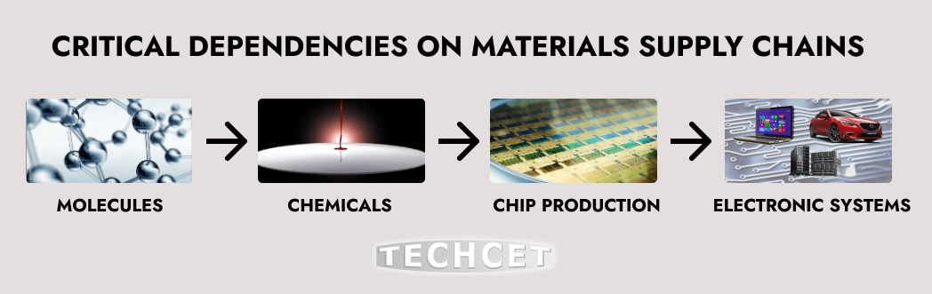
With recent chip shortages, various producers around the world have announced plans to invest in chip expansions that total more than US$500B over the next five years. For the US alone, this equates to an increase of >45% in semiconductor wafer starts by 2026. While this sounds hopeful for resolving chip deficiencies, it still does not address one key weakness: material shortages. As the industry expands, the risk of complications to the semiconductor supply chain grows, elevating the importance for material supply chain tracking and analysis.

Sulfuric acid is one example of an essential material that would put the semiconductor supply chain at risk if its supply is not properly managed. Fortunately, TECHCET has identified a >50% increase in demand for US sulfuric acid by 2026 to help key chip fabs prepare for expansions. TECHCET consistently provides key metrics related to supply and demand to the Critical Materials Council (CMC), a consortium formed in the mid-1990’s made up of chip fabricators and material suppliers. The Council also provides feedback to TECHCET to direct their ongoing supply chain analysis work. Identifying materials-related disruptions, dependencies, and weaknesses within the supply-chain, are all key elements of TECHCET’s focus and benefits to the CMC subscriber members.

In recent years, material shortages from the Russia-Ukraine conflict and COVID-19 have proven to be high stress points for chip fabricators and material suppliers. For example, neon gas faced shortages at the onset of the Russia-Ukraine war, threatening the stability of semiconductor production and causing high anxiety among chip fabs. At the time, it was unknown how much the US and Asia relied on Ukraine for neon supply. TECHCET managed to uncover various dependencies on Ukrainian neon from different regions around the world, helping major chip companies re-evaluate and better stabilize their supply chains. During the COVID pandemic, sporadic and extreme ocean freight roadblocks also contributed to slowdowns in chip manufacturing. In response to these disruptions, CMC subscriber companies met with logistics and shipping port officials to improve mitigation strategies for further supply interruptions.

CMC member subscribers also gain insight into supply chain challenges from the CMC Seminar. The next one will be hosted in Taiwan (October 25) and will focus on current problems in the materials supply chain and future quality requirements. This event is one of several that brings conversation on supply issues to the forefront. These events connect the entire semiconductor ecosystem by providing essential information on critical materials needed by decision makers at chip fabricators, suppliers, and government. The current CMC chip fab subscribers include more than a dozen of the world’s largest chip makers. (Reference: https://cmcfabs.org)

Given the massive impact semiconductors have in our digital global society, there is a growing and persistent need to manage the coming supply-chain issues, especially with expectations for chip volume to sharply ramp come 2025-2026. Looking into the future, TECHCET and the CMC will continue to facilitate coordination among key players in the materials and chip industry to navigate what lies ahead.

For more information on TECHCET: https://techcet.com or https://cmcfabs.org/2023-cmc-seminar/.

Lita Shon-Roy is President/CEO of TECHCET CA LLC, an advisory services firm expert in market analysis and business development of electronic markets and supply-chains for the semiconductor, display, solar/PV, and LED industries.

Sachi Brown is the Marketing Specialist of TECHCET CA LLC, in charge of marketing communications.

Wednesday, September 27, 2023

Forge Nano and KULR Partner for Cutting-Edge Battery Safety & Performance

In a significant move to enhance battery safety and efficiency, KULR Technology Group, a key player in sustainable energy management, has formed a strategic partnership with Forge Nano, renowned for its precision nanocoating technology. This alliance, estimated to be worth between $3.5 million to $5 million, will amalgamate KULR ONE Design Solutions - which offers advanced battery cell screening - with Forge Nano’s Atomic Layer Deposition (ALD) coating technique.


The collaboration begins with an assessment of Forge Nano’s elite battery cells intended for space and the US Department of Defense (DoD). KULR's innovative automated cell screening will be instrumental in gauging various battery cell parameters, ensuring they adhere to stringent NASA flight specifications.

In light of the recent announcement by the U.S. Department of Energy about a second tranche of $3 billion funding for battery production and recycling, this partnership positions itself as a catalyst in setting new benchmarks in battery safety and performance. 

Forge Nano, after securing $50 million earlier this year, has been aggressively investing in augmenting its battery production capacities. While KULR, with its expansive market presence in diverse sectors, sees this collaboration as a strategic alignment towards advancing the future of energy storage.

Source: Forge Nano and KULR Form a Strategic Partnership for Enhanced Battery Safety and Performance - Forge Nano

Tuesday, September 26, 2023

Unlocking the secrets of conformality, Characterization

Are you eager to learn more about 3D thin films Characterization in high aspect ratio structures and the tools essential for achieving this? The most insightful answers will be provided from high level experienced thin film characterization expert Dr. Jennifer S. Emara, the thin film characterization specialist at Fraunhofer IPMS and Dr. Jussi Kinnunen, the Optical measurement specialist at Chipmetrics.

Event Timing: Sept 28th, 2023. 5 pm CET (Europe), 8 am PST (USA)

Contact us at (+358417401098) or info@chipmetrics.com


TechInsights Discovers Micron's Cutting-Edge D1β LPDDR5 16 Gb DRAM Chips in Apple iPhone 15 Pro: Setting a New Standard in Memory Technology

TechInsights has confirmed Micron's cutting-edge D1β LPDDR5 16 Gb DRAM chips in the Apple iPhone 15 Pro, marking the industry's first venture into the D1β generation. These chips are smaller and denser than their predecessors, showcasing significant advancements in DRAM technology. Notably, Micron has achieved this without utilizing Extreme Ultraviolet Lithography (EUVL), a technique employed by competitors like Samsung and SK Hynix for their DRAM processes. This achievement highlights Micron's dedication to pushing the boundaries of DRAM technology, emphasizing innovation and efficiency in the tech landscape. Micron's groundbreaking D1β LPDDR5 16 Gb DRAM chip promises to reshape the future of memory technology, setting a new standard for the industry.

(Source Micron.com)

1-BETA includes cool stuff

High-k/Metal Gate

Micron's 1β fabrication process uses the company's 2nd generation high-K metal gate (HKMG) and is said to increase bit density of a 16Gb memory die by 35% as well as to improve power efficiency by 15% when compared to a similar DRAM device made on the company's 1α node

Pitch multiplication without the need for EUV Lithography

Micron's use of proprietary multi-patterning lithography involves advanced techniques for defining circuit patterns on semiconductor wafers with the highest precision. This approach allows Micron to create intricate patterns on the chips, achieving higher memory capacity in a smaller footprint. It enables the company to fit billions of memory cells on a chip that's roughly the size of a fingernail. 

While the semiconductor industry has been transitioning to extreme ultraviolet lithography (EUVL) to overcome technical challenges in patterning, Micron has opted for its multi-patterning lithography approach. This choice showcases Micron's expertise and innovation in lithography techniques, enabling them to continue shrinking circuit features and achieving greater memory capacity without relying on EUVL, which is still considered an emergent technology. 

By using proprietary multi-patterning lithography, Micron not only reduces the cost per bit of data but also enables devices with small form factors, such as smartphones and IoT devices, to incorporate more memory into compact spaces. This approach underscores Micron's commitment to staying at the forefront of memory technology innovation.
"While the industry has begun to shift to a new tool that uses extreme ultraviolet light to overcome these technical challenges, Micron has tapped into its proven leading-edge nano-manufacturing and lithography prowess to bypass this still emergent technology. Doing so involves applying the company’s proprietary, advanced multi-patterning techniques and immersion capabilities to pattern these minuscule features with the highest precision," Micron explains. Thy Tran, VP Process Integration, Micron


On the heels of the news that Micron has begun shipping QS-sample LPDDR5X components developed on the new 1-beta DRAM process node to its smartphone customers, host Jim Greene welcomes Thy Tran, Vice President of DRAM Process Integration, to the Chips Out Loud Podcast to discuss the emergent technology.

Sources:

Micron LPDDR5 16 Gb Non-EUVL Chip Found in Apple iPhone 15 Pro | TechInsights

LPDRAM | LPDDR | Micron Technology

Micron Ships World’s Most Advanced DRAM Technology With 1-Beta Node | Micron Technology


(Source: TechInsights.com)


Monday, September 25, 2023

Silicon Photonics: Illuminating the Future of High-Speed Data Centers and AI

Silicon photonics technology is fast becoming the linchpin in the quest to meet the soaring demands for data center bandwidth, with a particular focus on its application in artificial intelligence (AI) and machine learning (ML). This transformative technology leverages the power of photons to create efficient interconnections within data centers, a development recognized by experts at imec, a leading semiconductor research lab, as increasingly crucial.


In the imminent future, silicon photonics is set to revolutionize chip-to-chip connectivity among central processing units (CPUs), graphics processing units (GPUs), and other core computational elements at the heart of data centers and AI supercomputers. Despite formidable challenges in tightly integrating optics and electronics, the semiconductor industry is rising to the occasion, epitomized by the development of switch chips featuring co-packaged optics. imec envisions substantial enhancements in the power efficiency, bandwidth density, and cost-effectiveness of silicon photonics, potentially paving the way for advanced co-packaged optics, such as "wafer-level optical interconnects," capable of achieving near-light-speed data transfer between chips on printed circuit boards (PCBs) or within packages. 

Source: Silicon Photonics Will Shine in the Age of AI | Electronic Design


In summary, silicon photonics stands as a pivotal solution to address the burgeoning bandwidth requirements of data centers, with a particularly promising role in the realm of AI and ML applications. imec's concerted efforts in advancing this technology promise to shape the future of high-speed optical interconnect networks, ushering in an era of unprecedented computational capabilities.

NEO Semiconductor Unveils Revolutionary 3D NAND and DRAM Innovations at Flash Memory Summit 2023

NEO Semiconductor, known for its expertise in 3D NAND flash and DRAM technologies, presented groundbreaking innovations at Flash Memory Summit 2023 in August. The full presentation can be seen on Youtube (below). CEO Andy Hsu's keynote introduced their latest creation, 3D X-DRAM™, designed to overcome DRAM's capacity limitations and replace 2D DRAM. This technology utilizes the existing 3D NAND flash process with minor modifications, streamlining development and reducing costs. Hsu also unveiled a new AI application, "Local Computing," promising a substantial enhancement in AI chip performance.


X-DRAM™ significantly reduces data latency and provides ultra-high data throughput to unleash the full potential of High-Bandwidth Memory (HBM). HBM uses many Through Silicon Via (TSV) to increase I/O bandwidth. However, the HBM data latency remains almost the same when using conventional DRAM because bit line lengths remain the same.

Furthermore, NEO Semiconductor showcased various novel memory structures derived from 3D X-DRAM™, tailored for applications like 3D NOR flash memory, 3D Ferroelectric RAM (FFRAM), 3D Resistive RAM (RRAM), 3D Magnetoresistive RAM (MRAM), and 3D Phase Change Memory (PCM). These innovations enable the transition from 2D to 3D memory cells.


Hsu underscored the significance of these technologies for the semiconductor industry, cloud providers, and enterprises, highlighting that 3D X-DRAM™ offers a high-speed, high-density, cost-effective, and high-yield solution.

The presentation addressed the challenges faced by DRAM and NAND flash memory in the context of AI applications and introduced two innovative solutions – 3D X-DRAM™ and 3D X-NAND™.

Being part of the prestigious Flash Memory Summit, NEO Semiconductor showcased its technologies at booth number 215, and interested parties had the opportunity to schedule meetings with the company at the event.

In summary, NEO Semiconductor unveiled groundbreaking advancements in 3D NAND flash and DRAM technologies at Flash Memory Summit 2023, offering solutions to critical challenges in memory performance and capacity.

Source: NEO Semiconductor to Present Its Ground-Breaking 3D NAND and 3D DRAM Architectures in Keynote Address at Flash Memory Summit 2023 - Neo Semiconductor | X-Nand


Sunday, September 24, 2023

Stockholm-Based GREEN14 Leads the Charge in Sustainable Silicon Production for Solar Industry

Stockholm-based GREEN14 is making strides in its mission to revolutionize solar-grade silicon production. Following a successful lab-scale feasibility study, the company is set to establish a pilot plant using a pioneering quartz reduction process with hydrogen plasma. Emissions are expected to decrease by 60% to 95%, aligning with the company's commitment to sustainability. The technoeconomic analysis suggests the pilot plant will be economically viable, potentially transforming the solar industry. The plant, scheduled to be commissioned at KTH, signifies GREEN14's dedication to academic collaboration and clean energy innovation. Founder Adam Podgorski anticipates a significant positive environmental impact.

Green 14 is pioneering a sustainable shift in silicon production methods, potentially revolutionizing the solar panel manufacturing industry. Their innovative approach, protected by a patented solution, seeks to redefine how silicon is extracted from quartz. Unlike the traditional reliance on coal, Green 14 utilizes green hydrogen, a cleaner energy source, to convert silicon dioxide into silicon. This transition significantly reduces energy consumption and replaces carbon dioxide emissions with water vapor, offering a more environmentally friendly alternative.


"This is what the initial design of a reactor producing the world's first kg/hour of green solar grade silicon looks like. When we succeed we will have silicon with up to 95 percent GHG reduction at a cost lower than the leading Chinese producers." Source Green14 LinkedIn.

Green 14's primary goal is to reduce the carbon footprint associated with solar panel production, addressing the inherent environmental challenges in the industry. In a world where fossil fuels dominate manufacturing processes, Green 14's commitment to eco-conscious innovation signifies a potential shift toward a greener future.

Their recent successful lab tests mark a promising step forward. However, their most significant project lies ahead—an ambitious eight-meter-high test reactor set to be constructed at the Department of Materials Science at KTH. This project aims to scale up production and transition from batch processing to a more efficient continuous manufacturing process. The ultimate objective is to produce high-purity silicon on a larger scale, potentially setting new industry standards.


While Green 14 maintains the confidentiality of their innovative technology, their use of hydrogen plasma as a reducing agent and operation at temperatures of 3,000 degrees Celsius underline their commitment to technological advancement. The hope is that this approach will not only prove cost-effective but also more energy-efficient and environmentally sustainable compared to prevalent manufacturing methods, which often rely heavily on fossil fuels and are largely concentrated in China.

The estimated cost of the pilot facility at 20 million Swedish kronor reflects Green 14's earnest endeavor to introduce this transformative technology. Pending grant approvals from the Swedish Energy Agency and Vinnova, Green 14 is poised to make a significant impact on the future of solar panel manufacturing. The pilot facility, expected to commence operations soon, signifies a pivotal step toward a more sustainable and cleaner energy future.

About GREEN14
GREEN14 is a pioneering technology company committed to developing innovative solutions for a sustainable future. With a focus on renewable energy, GREEN14 is revolutionizing the production of solar grade silicon through its groundbreaking quartz reduction process. By combining cutting-edge technology with a commitment to environmental stewardship, GREEN14 is driving the transition to a low-carbon economy and paving the way for a cleaner, brighter future.

Friday, September 22, 2023

Kokusai Electric's Upcoming IPO: A Strategic Move in the Booming Semiconductor Market

Kokusai Electric is set to go public on the Tokyo Stock Exchange on October 25th, with an indicative share price of 1,890 yen per share. The IPO aims to raise 111.2 billion yen ($749.88 million) to fund research investment in the chipmaking equipment market. This move also serves as a partial exit for KKR, which previously purchased Hitachi's electronic equipment unit in 2017 and later spun off Kokusai.

In 2019, KKR attempted to sell Kokusai to Applied Materials for $3.5 billion, but the deal fell through due to regulatory hurdles in China. Applied Materials subsequently acquired a 15% shareholding in Kokusai. Kokusai Electric specializes in semiconductor manufacturing equipment, particularly in Atomic Layer Deposition (ALD) technology, with a strong market position, including a 23% share of the global ALD equipment market in 2020.


Kokusai Electric's ALD equipment portfolio includes products like TSURUGI-C²® for 300mm wafers and VERTRON® Revolution for 200mm wafers, known for their high performance and productivity. The company's main customers for ALD equipment include Samsung, SK Hynix, Micron, and Intel. Kokusai Electric's IPO is scheduled for September 23, 2023.

ASML's 2023 Outlook: Surging Ahead in Semiconductor Equipment Despite Challenges and Export Controls

In 2023, ASML, the leading semiconductor lithography equipment supplier, is set to achieve remarkable success, outpacing its rivals and emerging as the number 1 provider of Wafer Fabrication Equipment. Boasting an impressive 30% revenue growth forecast for the year, ASML is thriving amidst an industry landscape marked by its consistent performance. With a substantial backlog of cutting-edge Deep Ultraviolet (DUV) and Extreme Ultraviolet (EUV) systems and surging demand from China, ASML's growth continues despite hurdles like supply chain disruptions and regulatory changes, ASML remains a beacon of innovation and resilience in the semiconductor sector.

By Abhishek Kumar Thakur and Jonas Sundqvist

ASML, a leading supplier of semiconductor equipment, is poised for a significant year in 2023, projected to surpass Applied Materials (AMAT) as the top provider of Wafer Fabrication Equipment. This achievement is attributed to ASML's robust revenue growth, expected to reach a remarkable 30% increase in 2023, while Applied Materials faces a decline of 20% according to Seeking Alpha*. ASML's success can be attributed to a substantial backlog of Deep Ultraviolet (DUV) and Extreme Ultraviolet (EUV) systems, driven by heightened demand in China.

* Fact check: Due to strong DUV revenue and despite the increased uncertainties, ASML expects strong growth for 2023 with a net sales increase towards 30% and a slight improvement in gross margin, relative to 2022. ASML Holding revenue for the twelve months ending June 30, 2023 was $27.293B, a 25.97% increase year-over-year. AMAT revenue is estimated to increase by 2.6% to 26.33 B. Meaning ASML would pass bu end of 2023.

https://finance.yahoo.com/quote/AMAT/analysis/ 


Despite facing challenges like supply chain disruptions and a factory fire, ASML has consistently ranked among the top three semiconductor equipment suppliers since 2017. Their backlog of EUV systems, combined with growing acceptance of DUV tools, contributes to their strong performance.

However, potential headwinds include supply chain concerns, past issues like the Berlin factory fire, and looming sanctions affecting exports to China. While ASML has addressed some challenges, the possibility of US sanctions in 2024 poses a threat to its growth.

Furthermore, ASML now faces new export controls imposed by the Netherlands, impacting shipments to China. While the company downplays these controls' immediate financial impact, they are expected to affect specific DUV systems, adding to global efforts to limit China's semiconductor advancements.

In this volatile landscape, ASML's ability to adapt to evolving regulations and maintain its technological leadership will be crucial. The impact of these restrictions, especially on shipments to China, could influence the company's growth trajectory in the semiconductor industry. Despite these challenges, ASML remains a prominent player with significant potential in the semiconductor equipment market.

ASML is set to deliver the industry's first High-NA extreme ultraviolet (EUV) lithography scanner by the end of 2023, marking a significant development for advanced chip manufacturing. The Twinscan EXE:5000 pilot scanner with a 0.55 numerical aperture (NA) will enable chipmakers to explore High-NA EUV technology. This innovation is crucial for achieving an 8nm resolution, suitable for manufacturing technologies beyond 5nm nodes. Intel is expected to be the first customer, but integration and adoption details are still uncertain. This advancement requires substantial investments, with reports suggesting costs of $300-400 million per unit.

To add some colour, initially, Intel had plans to employ ASML's High-NA tools for its 18A (1.8 nm) production node, scheduled for high-volume manufacturing in 2025, aligning with ASML's Twinscan EXE:5200 delivery. However, Intel accelerated its 18A production, moving it to the latter part of 2024. This change in strategy involved the use of ASML's Twinscan NXE:3600D/3800E with two exposures and Applied Material's Endura Sculpta pattern-shaping system. The objective was to reduce reliance on EUV double patterning techniques. Applied Materials' Centura Sculpta is a pattern-shaping machine equipped with a unique algorithm that can manipulate patterns produced by an EUV scanner. It has the capability to stretch these patterns in a user-defined direction along the X-axis. This process effectively reduces the space between features and enhances pattern density. This means that moving ahead ASML and Applied Materials are entering an interesting competitive space previously not encountered.

ASMLs Products

As an background, ASML specializes in the production of cutting-edge lithography systems crucial for semiconductor manufacturing. Their product portfolio includes the following key offerings:

Extreme Ultraviolet (EUV) Lithography Machines: ASML's EUV lithography machines are at the forefront of semiconductor manufacturing technology. These machines use extremely short wavelengths of light to create intricate patterns on silicon wafers, enabling the production of advanced and smaller semiconductor chips. EUV technology is essential for next-generation processors and memory chips.

Deep Ultraviolet (DUV) Lithography Machines: DUV lithography systems are another vital component of ASML's product lineup. They use longer wavelengths of light compared to EUV and are employed for a wide range of semiconductor applications, including memory and logic chip production. ASML's DUV systems are known for their precision and reliability.

TWINSCAN Series: Within the DUV lithography category, ASML offers the TWINSCAN series, which includes machines like the TWINSCAN NXT:2000i, NXT:2050i, and NXT:2100i. These systems are designed for immersion lithography, where the wafer and the lens are submerged in a liquid, enhancing precision and resolution.

EUV High Numerical Aperture (NA) Systems: ASML has been advancing its lithography machines by increasing the numerical aperture (NA), a key parameter that affects resolution. High-NA systems are capable of printing even smaller features on semiconductor wafers, enabling the production of highly advanced chips.

ASML's lithography machines are considered critical infrastructure for semiconductor manufacturing, and the company's technological leadership in this area has positioned it as a dominant player in the industry. The company's ability to innovate and adapt its lithography systems to meet the ever-increasing demands of semiconductor manufacturers has been a key factor in its success and growth prospects. However, the recent export controls and geopolitical pressures, particularly concerning shipments to China, introduce additional challenges and uncertainties for ASML and its specialized products.

Sources:

ASML Hit With New Dutch Limits on Chip Gear Exports to China - Bloomberg

ASML To Top WFE Semiconductor Equipment In 2023, Topping Applied Materials | Seeking Alpha

ASML to ship first pilot tool in its next product line in 2023, CEO says | Reuters

ASML to Deliver First High-NA EUV Tool This Year (anandtech.com)

EUV Alternative Speeds Up Chip Production - EE Times

BALD Engineering - Born in Finland, Born to ALD: ASML Remains on Track to Deliver High NA EUV Machines in 2023

BALD Engineering - Born in Finland, Born to ALD: Netherlands' chip tool export controls take effect for DUV Lithography and ALD

BALD Engineering - Born in Finland, Born to ALD: Applied Materials’ Pattern-Shaping Technology - Centura Sculpta


Wednesday, September 20, 2023

Linköping University Researchers Uncover Challenges in Thermal ALD of Indium Nitride (InN)

Researchers from the Pedersen Group at Linköping University have investigated the limitations of thermal atomic layer deposition (ALD) for indium nitride (InN). Using quantum-chemical density functional theory calculations, they explored the adsorption process of ammonia (NH3) on InN and compared it to gallium nitride (GaN), shedding light on the challenges in InN deposition.

InN holds promise in semiconductor and electronics applications due to its distinctive properties. It boasts a high electron mobility, exceeding that of many other III-nitride materials, rendering it suitable for high-frequency electronic devices like transistors and amplifiers. With a narrow bandgap of around 0.7 eV, InN finds applications in infrared photodetectors and optoelectronic devices. Despite challenges in thermal stability during deposition, it exhibits good stability when appropriately processed, making it valuable in high-temperature electronics. Its high electron velocity enhances the performance of high-speed field-effect transistors. InN also shows potential in energy-efficient electronics and gas sensing applications, furthering its significance in the semiconductor and electronics industry.

The deposition of indium nitride (InN) using CVD is challenging due to its low thermal stability, which limits the use of high-temperature processes. ALD is an alternative method that can operate at lower temperatures. While ALD has been successful in depositing materials like aluminum nitride and gallium nitride (GaN) using ammonia as a nitrogen precursor in thermal processes, InN can only be deposited using plasma ALD. This suggests a limitation to thermal ALD with ammonia for InN.


Gibbs free energy profile for the adsorption of NH3 onto InN and GaN at 500 (a) and 800 K (b).

Researchers used quantum-chemical density functional theory calculations to investigate the adsorption process of ammonia (NH3) on both GaN and InN surfaces. They aimed to understand if differences in this process could explain why thermal ALD of InN is challenging. Their findings revealed a similar reactive adsorption mechanism on both materials, where NH3 adsorbs onto vacant sites created by the desorption of methyl groups from the surfaces. However, the energy barrier for this adsorption process was significantly higher on InN compared to GaN, indicating that the process is much slower on InN.

This slow kinetics would hinder NH3 from effectively adsorbing onto InN during the ALD growth process, making thermal ALD with InN using NH3 impractical. As a result, the only alternative to a fully thermal ALD process for InN appears to be using a different precursor system due to InN's thermal instability.

Source: On the limitations of thermal atomic layer deposition of InN using ammonia | Journal of Vacuum Science & Technology A | AIP Publishing

Plasma-Therm Strengthens Power Electronics Presence with Acquisition of Thin Film Equipment SrL

Plasma-Therm, a prominent manufacturer of plasma-process equipment for the semiconductor industry, has announced its acquisition of Thin Film Equipment SrL (TFE) on September 18, 2023. TFE, based in Binasco, Italy, specializes in supplying sputtering equipment for semiconductor research and production, particularly in physical vapor deposition (PVD) sputtering and evaporation process equipment and high purity materials for thin film applications.

This acquisition is part of Plasma-Therm's strategy to expand its presence in Europe and strengthen its position in the power device market. TFE's suite of PVD tools, catering to MEMS, Power, RFID, and other semiconductor applications, complements Plasma-Therm's existing product portfolio in etch and deposition. Additionally, TFE's expertise in PVD technology enhances Plasma-Therm's customer service and support capabilities.

The power semiconductor market is expected to grow substantially, reaching $6.3 billion by 2027, according to The Yole Group's "Power SiC 2022" report. Plasma-Therm is well-positioned to support this growth with the acquisition of TFE and its MRC Eclipse product line.

TFE will continue to operate independently but will collaborate closely with Plasma-Therm to offer a more comprehensive range of plasma and PVD process technology solutions to customers. This acquisition will also enable both companies to expand their R&D resources and global customer service and support teams.

Plasma-Therm is a global manufacturer of advanced plasma processing equipment, serving various industries, including wireless, power devices, MEMS, photonics, advanced packaging, and data storage. It has locations in North America, Europe, and Asia-Pacific.

TFE SrL, founded in 1996, is a leading supplier of sputtering equipment for R&D and production, known for its flexibility, reliability, process knowledge, and a large worldwide installed base.

Source: Plasma-Therm Announces Acquisition of Thin Film Equipment (globenewswire.com)

Tuesday, September 19, 2023

Aixtron’s G10-SiC CVD System Supports GlobiTech’s SiC Epitaxy Expansion

  • GlobiTech Inc produces silicon carbide (SiC) and silicon epitaxial wafers, primarily focusing on serving the power and electric vehicle (EV) market segments.
  • GlobiTech Inc's production facilities are located in Sherman, Texas, USA.

Aixtron SE is aiding Texas-based silicon-epitaxy foundry GlobiTech Inc's entry into the silicon carbide (SiC) epitaxy market. The G10-SiC chemical vapor deposition (CVD) system from Aixtron has enabled GlobiTech to rapidly scale SiC epitaxy production in response to growing demand for power epiwafers. Featuring dual wafer sizes (9x150mm and 6x200mm), it offers high throughput per fab space. GlobiTech's expansion confirms the trend of SiC replacing silicon in various applications. Both firms have enjoyed a fruitful partnership, with Aixtron's tools maximizing wafer output. The G10-SiC is projected to be Aixtron's top-selling product in 2023.


Aixtron G10-SiC (Source Aixtron.com)

Source: AIXTRON Pressemeldungen :: AIXTRON

Recent Blog posts on SiC:

BALD Engineering - Born in Finland, Born to ALD: SiC Market Soars Towards $9 Billion: EVs and High-Power Chargers Drive Growth

BALD Engineering - Born in Finland, Born to ALD: SiC Market Soars Towards $9 Billion: EVs and High-Power Chargers Drive Growth

BALD Engineering - Born in Finland, Born to ALD: Samco launches new ICP Tornado Plasma ALD system

BALD Engineering - Born in Finland, Born to ALD: ASM International has completed the acquisition of Italian Silicon Carbide Equipment Manufacturer LPE S.p.A.

BALD Engineering - Born in Finland, Born to ALD: Chemistry paves the way for improved electronic materials - LiU have developed a new molecule that can be used to create high-quality indium nitride

Background:

  • Silicon carbide: from gold rush to commodity?1, which provides an overview of the global SiC market and its predictions for the future of the technology. It discusses the growth rate, size, and drivers of the SiC device market, as well as the competitive landscape and supply chain of the SiC industry. It also analyzes the challenges and opportunities for SiC technology in different applications, such as automotive, industrial, energy, and telecommunications. It also compares and evaluates SiC with other wide bandgap materials, such as gallium nitride (GaN) and diamond.
  • The 2023 global fab landscape: opportunities and obstacles2, which considers the state of the global semiconductor fab market in a post-COVID world. It discusses the emerging business models that could enable the semiconductor industry to migrate to leading-edge and mature technology with optimal manufacturing capacity. It also examines the impact of COVID-19, trade wars, and geopolitical tensions on the semiconductor supply chain and fab investments. It also explores the trends and innovations in semiconductor materials, devices, and modules, such as silicon carbide (SiC), gallium nitride (GaN), and quantum computing.


AIXTRON's MOCVD Machine Advancing 2D-Materials at imec

AIXTRON, a German semiconductor equipment manufacturer, has successfully installed the CCS 2D Metal-Organic Chemical Vapour Deposition (MOCVD) reactor at the Interuniversitair Micro-Electronica Centrum (imec) in Belgium. Part of the 2D Experimental Pilot Line initiative, this reactor facilitates large-scale epitaxial deposition of 2D-materials on 200/300 mm wafers, marking a significant milestone in the transition of these materials from lab to fab.

Inge Asselberghs, Director of the 2D Experimental Pilot Line at imec, emphasizes the unique position of imec as a bridge between academia and industry, offering access to both fundamental research laboratories and industrial infrastructure.

Salim El Kazzi, 2D Product Manager at AIXTRON, outlines the challenges of the lab-to-fab transition, including miscommunication and the technical intricacies of 2D-materials. AIXTRON addresses these challenges by fostering collaboration among top researchers and providing FAB-compatible reactors like the CCS 2D.

To bridge the gap effectively, Asselberghs highlights the importance of versatile tools for rapid material and process screening, crucial for seamless information exchange between industry and academia.

The CCS 2D MOCVD machine from AIXTRON offers precise control over deposition parameters and features like closed-coupled shower heads and a transfer module for 2D-material growth on 300 mm wafers.


This installation promises exciting prospects for imec's research on transition metal dichalcogenides (TMDCs) and advances in pilot-line processes for 2D-material growth and layer transfer. Both AIXTRON and imec actively participate in Graphene Week 2023, contributing to the advancement of 2D-materials in industrial applications and strengthening the link between academia and industry.

Source: AIXTRON installs a MOCVD machine CCS 2D in IMEC’s fab | Graphene Flagship (graphene-flagship.eu)

Friday, September 15, 2023

Tokyo Electron Integrated Report/Annual Report 2023 available for download

Tokyo Electron (TEL) issues an integrated report for the purpose of reporting our medium- to long-term profit expansion and continuous corporate value enhancement to their stakeholders.

As they celebrate their 60th anniversary this year, the 2023 report looks back at the history of our business expansion. It also details our efforts to continuously create value by the value chain of their business activities anchored around material issues, in conjunction with their sustainability initiatives.

For anyone involved in the semiconductor industry or those eager to gain fresh perspectives in this dynamic field, this report is a must-read. It not only showcases TEL's history and strategies but also sheds light on industry trends, sustainability practices, and the exciting developments shaping the future of semiconductor technology. Dive into this comprehensive report and unlock valuable knowledge about TEL's journey and the semiconductor industry at large.


TEL also have great training material and a Nanotech Museum:


Wednesday, September 13, 2023

Global Fab Equipment Spending to Rebound in 2024 After 2023 Slowdown, Predicts SEMI Report

Global fab equipment spending is anticipated to decline by 15% in 2023, dropping to $84 billion from the record high of $99.5 billion in 2022. However, a recovery of 15% to $97 billion is expected in 2024, driven by the end of a semiconductor inventory correction in 2023 and increased demand in high-performance computing (HPC) and memory segments. The foundry segment will lead the industry's expansion in 2023 with $49 billion in investments, while memory spending is set to make a strong comeback in 2024 with a 65% increase to $27 billion. 


Taiwan will remain the top region for fab equipment spending in 2024, with $23 billion, followed by Korea with $22 billion, and China in third place at $20 billion. The Americas and Europe/Mideast regions are also expected to see increased investments, while capacity growth in the global semiconductor industry is forecasted to continue, rising by 6% in 2024.

Intel to Sell 10% Stake in IMS Nanofabrication to TSMC for $4.3 Billion

Intel will sell a 10% stake in IMS Nanofabrication to TSMC, valuing IMS at $4.3 billion, maintaining Intel's majority ownership. IMS leads in multi-beam mask writing tools for advanced extreme ultraviolet lithography, crucial for AI and mobile applications. This investment enhances IMS' independence and fosters innovation, including high-numerical-aperture EUV technology. The deal is set to close in Q4 2023. IMS is vital for semiconductor industry growth, with the market projected to reach $1 trillion by 2030. Intel acquired IMS in 2015 and sold a 20% stake to Bain Capital earlier in 2023, while TSMC's partnership with IMS dates back to 2012.


About IMS Nanofabrication

IMS Nanofabrication Global, LLC, a majority-owned subsidiary of Intel Corporation, is the global technology leader for multi-beam mask writers. Its customers are the largest chip manufacturers in the world, who rely on its technology to produce current and future chip generations. IMS’ innovative multi-beam writers play a key role in chip manufacturing and provide significant added value to the semiconductor industry. They are continually customized and refined by an interdisciplinary team, in line with the latest market demands. Over the last 10 years, IMS has perfected its electron-based multi-beam technology. The first-generation multi-beam mask writer, MBMW-101, is successfully operating all over the world. The second-generation multi-beam mask writer, MBMW-201, entered the mask writer market in the first quarter of 2019 for the 5nm technology node. And this year, IMS is launching MBMW-301, a fourth-generation multi-beam mask writer that delivers unprecedented performance. Learn more at www.ims.co.at/en/.

Monday, September 11, 2023

Exploring SMIC's 7nm Semiconductor Advancements: Technology, Dimensions, and Future Prospects

The recent introduction of Huawei's Mate 60 Pro smartphone, featuring a 7 nm chip from Semiconductor Manufacturing International Corp. (SMIC), has raised questions about the authenticity of SMIC's technological strides and their implications. This summary dives into the heart of SMIC's 7 nm technology, shedding light on its dimensions, technological intricacies, challenges, and the outlook for the future.

However, it has been known for some time that SMIC has been developing at putting out 7 nm chips, and an early 2022 assessment published at Seeking Alpha can be found here: Applied Materials: SMIC Move To 7nm Node Capability Another Headwind (NASDAQ:AMAT) | Seeking Alpha

The SMIC 7 nm Technology Debate

Central to the debate surrounding SMIC's technology is the classification of whether it genuinely qualifies as 7 nm. Parameters such as Fin Pitch (FP), Contacted Poly Pitch (CPP), and Metal 2 Pitch (M2P) are scrutinized. While SMIC's FP pitches are larger than TSMC's 10 nm, its CPP and M2P dimensions match TSMC's 10 nm, creating a complex classification.

SMIC appears to have a serviceable first generation 7nm process now with a reasonable prospect to get to second generation 7nm/6nm in the near futures. 5nm and 3nm while theoretically possible would be highly constrained and expensive process versions if pursued due to the lack of EUV. - Scotten Jones, SemiWiki (LINK)

Design Technology Co-Optimization (DTCO) Features

SMIC's 7 nm process introduces Design Technology Co-Optimization (DTCO) features uncommon in traditional 10 nm processes. Notably, SMIC's track height is smaller than TSMC and Samsung's 10 nm processes, approaching 7 nm-class characteristics. These features add to the nuanced evaluation of SMIC's technological position.

Cell Density and Cut Masks

SMIC's high-density logic cell boasts an impressive 89 million transistors per millimeter squared, akin to Samsung and TSMC's first-generation 7 nm processes. This suggests that SMIC's technology aligns with the 7 nm category, though the debate on its dimensions continues. Notably, SMIC's process introduces larger Contacted Poly Pitch (CPP) dimensions, hinting at potential performance challenges that necessitated this adjustment.

The EUV Challenge and Future Prospects and Alternative Technologies

SMIC's journey toward further technological advancements faces significant hurdles due to the unavailability of extreme ultraviolet lithography (EUV) systems in China. EUV technology plays a pivotal role in pushing semiconductor boundaries. However, ongoing US restrictions on EUV system shipments to China constrain SMIC's options for achieving cutting-edge technology.

Self aligned multi patterning (SAMP) in Advanced Logic Semiconductor Manufacturing

In advanced logic semiconductor manufacturing, addressing the challenges posed by sub-5 nm nodes and dense metal layers is essential. SMIC can consider alternative technologies like Atomic Layer Deposition (ALD) and Directed Self-Assembly (DSA) to overcome these hurdles.

ALD stands out for its precision in depositing thin films, allowing for the creation of ultra-thin etch masks, spacers, and precise control over critical dimensions. On the other hand, DSA leverages materials' self-assembly properties to form predefined patterns, effectively dividing pitch sizes and simplifying lithography masks.

Incorporating ALD and DSA into semiconductor manufacturing processes has the potential to enhance the capabilities of immersion lithography, enabling smaller nodes without the need for EUV lithography. While these technologies require further research and development, they offer promise in helping semiconductor manufacturers advance their technology and remain competitive, particularly in the absence of EUV lithography equipment.

Together with self-aligned multi-patterning (SAMP) techniques like self-aligned double patterning (SADP), self-aligned quadruple patterning (SAQP), and self-aligned litho-etch-litho-etch (SALELE), these alternative approaches provide SMIC with a range of options to navigate the complexities of advanced semiconductor manufacturing, ultimately shaping the future of Chinese advanced chip fabrication.

The Future of Nanoimprint Lithography: High-Volume Production Possibilities

Nanoimprint lithography (NIL) offers potential for high-volume production with sub-10 nm resolution, revolutionizing semiconductor manufacturing. TEL and Canon have showcased NIL's sub-10 nm capabilities, making it suitable for multiple memory generations using a single mask. Challenges like edge placement errors (EPE) are addressed through precision techniques like Quasi-Atomic Layer Etch (Quasi-ALE). To achieve aggressive scaling targets, overlay accuracy and critical dimension uniformity (CDU) management are vital. NIL's simplicity and cost-effectiveness make it a promising contender, with ongoing development poised to refine its integration into semiconductor fabrication.

Future Outlook for SMIC and China

SMIC's path forward may involve alternative fabrication technologies such as ALD, DSA, and NIL. that offers the potential for high-volume production with sub-10 nm resolution.

By mastering and integrating these advanced technologies into semiconductor manufacturing could potentially expand immersion lithography's capabilities, accommodating smaller nodes without depending on EUV lithography. While further research and development are essential, these technologies offer potential pathways for SMIC to advance its fabrication processes and sustain competitiveness, particularly in the absence of EUV lithography equipment. These strategies, alongside self-aligned multi-patterning techniques, stand to influence the future of advanced chip fabrication in China beyond 7 nm. 

The answer is as always - it depends. For how long will China have access to also Immersion Lithography? Will top tier OEMs be allowed to continue to export ALD and other process technology needed to China? What will be the cost using higher complexity and additional masks needed for SAQP (cut masks)? Is Huawei's limited chip demand, as compared to Apple & Co, enough to pay for the R&D needed? Will Chinese state support cover the development and fab expansion cost? 

Sources:

193i Lithography Takes Center Stage...Again (semiengineering.com)

Does SMIC have 7nm and if so, what does it mean - SemiWiki

Look Inside Huawei Mate 60 Pro Phone Powered by Made-in-China Chip - Bloomberg

BALD Engineering - Born in Finland, Born to ALD: The Future of Nanoimprint Lithography: Exploring Possibilities and Challenges for High-Volume Production

BALD Engineering - Born in Finland, Born to ALD: Comparison confirms that SMIC reaches 7nm without access to western equipment & technologies

Applied Materials: SMIC Move To 7nm Node Capability Another Headwind (NASDAQ:AMAT) | Seeking Alpha

Saturday, September 9, 2023

Unlock the Future of Materials and Products: Join the MERCK ALD and ALE Innovation Webinar!

Join us for an exciting event on October 18, 2023: "Revolutionizing Materials and Products: Innovations in Atomic Layer Deposition (ALD) and Atomic Layer Etch (ALE)." Presented by Sergei Ivanov, Senior R&D Manager at Merck KGaA, and Martin McBriarty, Senior Scientist, this webinar promises groundbreaking insights into the world of materials and product innovation.

Event Details:

Date: October 18, 2023

Time: 4:00 pm - 5:00 pm CET

Host: Laith Altimime, President of SEMI Europe

Agenda:

- 4:00 pm CET - Welcome remarks by Laith Altimime, President, SEMI Europe.

- 4:05 pm CET - "Revolutionizing Materials and Products: Innovations in Atomic Layer Deposition (ALD) and Atomic Layer Etch (ALE)" by Sergei Ivanov & Martin McBriarty.

- 4:45 pm CET - Q&A session moderated by Laith Altimime, followed by conclusions from all speakers.

About the Speakers:

Sergei Ivanov: Sergei is the Senior R&D Manager in the Organometallics division of Thin Films Business. He leads a research program focused on developing novel precursors for the deposition of metal, metal nitride, and metal oxide films. Sergei holds a PhD in Inorganic Chemistry from Kurnakov Institute of Russian Academy of Sciences and a B.S. in Chemical Engineering from Mendeleev University of Chemical Technology.

Martin McBriarty: Martin is a Senior Scientist leading the development of atomic layer etch and other vapor-phase etch methods. He earned his B.S. in Materials Science & Engineering at the University of Florida and his Ph.D. in the same field at Northwestern University. Martin joined Intermolecular in 2018 after completing postdoctoral research at Pacific Northwest National Laboratory.


ATLANT 3D Hosts Workshops Unveiling Atomic Layer Advanced Manufacturing Innovation

Atlant 3D will hold a series of workshops happening from October 7th to 13th. We Open Door to ATLANT 3D to share our cutting-edge innovation in atomic layer processing, and we will show you insights on how atomic layer processing will become an atomic layer advanced manufacturing platform!
ATLANT 3D technology is our proprietary Microreactor 

Dive Deep into the World of Atomic Precision with ATLANT 3D!
Event by ATLANT 3D

Oct 7, 2023, 9:00 AM - Oct 13, 2023, 4:00 PM (CET)

Mårkærvej 2b, Taastrup, Region Hovedstaden, DK, 2630


Direct Atomic Layer Processing (μDALP), which works by sequentially applying reactive gases to a surface via a microreactor/micronozzle and generating self-controlled chemical reactions on the surface. Repeating this process in cycles enables rapid, direct, multi-material, atomically precise patterning and structuring on simple and complex surfaces, including semiconductor wafers and surfaces with existing structures and devices. Integrating multiple micronozzles in a single printhead allows increasingly complex structures to be fabricated through the simultaneous use of different materials and printing resolutions. 

ATLANT 3D equipment is built as modular units which gives compatibility across different platforms and technologies. It can work as a production line based on process modules and as a cluster tool-compatible module unit.


SkyWater Installs Advanced Atomic Layer Deposition System from Picosun

SkyWater Technology (SkyWater Technology | U.S. Semiconductor Manufacturer) has announced the installation of an Atomic Layer Deposition (ALD) system, the Applied Picosun MorpherTM, to offer advanced semiconductor processing capabilities to its customers. ALD is a precise method for depositing ultra-thin, uniform, and conformal material layers, making it ideal for applications like sensors and emerging memory technologies. SkyWater's Technology as a Service (TaaS) model allows customers to access this technology for developing and producing innovative technologies. The ALD tool has two thermal batch chambers for depositing metals and oxides, ensuring high-quality and repeatable results. This move aims to meet the increasing demand for ALD applications in semiconductor processing, particularly in areas such as biosensors, photonics, and extreme CMOS applications.


SkyWater Minnesota Fab (SkyWater)

SkyWater Technology is a leading U.S.-based semiconductor manufacturer with a unique Technology as a Service (TaaS) model. They offer a wide range of semiconductor solutions, serve various industries, and emphasize innovation and quality. Their expertise spans diverse semiconductor categories, from mixed-signal CMOS to photonics, and they are accredited as a Category 1A Trusted Foundry by the Defense Microelectronics Activity (DMEA).


The Morpher ALD tool is designed for precise and controlled deposition of thin material layers, making it suitable for various semiconductor applications. It is configured with two thermal batch chambers, one for depositing metals and another for depositing oxides, allowing for flexibility and efficiency in semiconductor fabrication processes. This tool is being installed at SkyWater Technology to provide their customers with access to ALD capabilities for developing and producing advanced semiconductor technologies.


Thursday, September 7, 2023

AIXTRON Unveils G10-GaN Cluster Solution for Power Electronics Market

AIXTRON SE has unveiled the G10-GaN cluster solution for high-volume manufacturing of Gallium Nitride (GaN) power and RF devices. The platform delivers superior performance, a compact design, and cost-efficiency. Dr. Felix Grawert, CEO of AIXTRON, highlighted its potential in reducing global CO2 emissions and its growing demand in applications like mobile fast chargers, data centers, and solar energy. The system improves material uniformity, extends equipment uptime, and offers a 25% cost reduction per wafer, making it a significant advancement in semiconductor technology.

Herzogenrath, September 6, 2023 – AIXTRON SE, the semiconductor industry's leading deposition equipment supplier, has introduced its latest innovation, the G10-GaN cluster solution for Gallium Nitride (GaN) based power and radio frequency (RF) devices. This groundbreaking platform is making its debut at SEMICON Taiwan (September 6-8, 2023) in Taipei, offering unparalleled performance, a compact design, and exceptional cost-efficiency.

The cluster can be equipped with up to three process modules, delivering a record capacity of 15x200 mm wafers thanks to Planetary batch reactor technology – enabling a 25 percent cost reduction per wafer compared to previous products. LINK

Dr. Felix Grawert, CEO and President of AIXTRON SE, proudly announced, "Our new G10-GaN platform has already received qualification for high-volume production of GaN Power devices from a prominent US device manufacturer. It delivers double the productivity per cleanroom area compared to our previous product, enhances material uniformity, and provides a competitive edge to our customers."

GaN-based technologies are gaining importance in the drive to reduce global CO2 emissions due to their significantly more efficient power conversion capabilities compared to traditional silicon (Si). GaN can reduce power losses by a factor of two to three. Dr. Grawert noted, "We anticipate continuous growth in the GaN market throughout this decade and beyond. GaN has already replaced silicon in fast chargers for mobile devices, and we are witnessing rising demand in data centers and solar applications."

AIXTRON has been at the forefront of GaN on Si process and hardware development for over two decades. The company's AIX G5+ C planetary reactor, known for being the first fully automated GaN Metal-Organic Chemical Vapor Deposition (MOCVD) system with In-Situ Cleaning and Cassette-to-Cassette automation, is now an industry-standard tool for GaN power production. The new G10-GaN cluster solution builds upon this legacy, elevating every performance metric.

Designed to maximize cleanroom space, the G10-GaN features innovative reactor inlets that enhance material uniformity, resulting in optimized device yields. The platform incorporates on-board sensors, a new software suite, and fingerprint solutions to ensure consistent performance across runs, even between maintenance cycles, extending equipment uptime by over 5% compared to the previous generation.

The cluster can accommodate up to three process modules, boasting a record capacity of 15x200 mm wafers thanks to Planetary batch reactor technology. This enables a remarkable 25% reduction in cost per wafer compared to previous products, a factor that promises significant savings for manufacturers.

AIXTRON's G10-GaN cluster solution positions the company as a key player in the ever-evolving landscape of GaN-based power and RF devices, furthering its commitment to advancing semiconductor technology for a sustainable future.

Wednesday, September 6, 2023

ASML Remains on Track to Deliver High NA EUV Machines in 2023

ASML, the leading semiconductor equipment manufacturer, is set to ship the first pilot tool from its next product line in 2023, despite some supplier delays, according to CEO Peter Wennink. These High NA EUV machines, crucial for top chipmakers to create smaller and better chips in the coming decade, will cost over $300 million euros each and provide up to 70% better resolution. ASML currently dominates the lithography market, a pivotal step in chipmaking, and is seeing strong demand for its older DUV machines, with 30% sales growth forecasted in 2023, primarily driven by Chinese customers.

ASML's High NA EUV machines are used by a range of prominent semiconductor manufacturers, including TSMC, Intel, Samsung, SK Hynix, and Micron. These chipmakers rely on ASML's cutting-edge lithography equipment to manufacture semiconductor chips, from microprocessors to memory chips.

"High NA" stands for "High Numerical Aperture." Numerical Aperture (NA) is a measure of the ability of an optical system, such as a lens or mirror, to gather and focus light. A higher numerical aperture indicates a greater ability to capture light and provide finer detail and resolution in imaging or lithography processes. ASML's High NA EUV machines, are designed to gather light from a wider angle compared to their previous generation tools. This wider angle collection of light allows for significantly improved resolution in the semiconductor manufacturing process, making it possible to create smaller and more advanced semiconductor chips with greater precision required for the Ångström Era - basically the sub 2 nm nodes.

Source:


TSMC's Silicon Photonics Investment Boosts AI Chip Efficiency for ChatGPT

Taiwan Semiconductor Manufacturing Co. (TSMC) is heavily investing in silicon photonics, combining silicon chips and optical tech to enhance AI applications like ChatGPT. TSMC, the world's top contract chipmaker, aims to improve AI chip performance through silicon photonics, addressing energy efficiency and computing power issues. This technology integrates optics with silicon-based circuits for high-speed, low-power data transmission. Silicon photonics attracts substantial investment across the semiconductor industry, impacting data centers, supercomputers, networking, and more. TSMC is developing integrated silicon photonics systems with advanced chip packaging technology but has not yet entered mass production. The global silicon photonics market is projected to grow to $7.86 billion by 2030.

Source:

Tuesday, September 5, 2023

Revolutionizing Pharmaceutical Packaging and Labware: ALD Technology Enhances Material Properties

Picosun, an Applied Materials company, is proud to announce a breakthrough in enhancing the properties of packaging materials and labware using Atomic Layer Deposition (ALD) technology. ALD offers impermeable barriers and functional surfaces, revolutionizing pharmaceutical packaging and labware for the better.

Date: 12th December Time: 3:00 PM London / 10:00 AM New York

As pharmaceutical packaging evolves to accommodate biological drugs and novel packaging solutions, ALD technology steps in to provide ultra-thin, uniform, and precise material layers with atomic-level thickness and composition. This innovation caters to the demands of primary packaging materials and labware, offering impermeable barriers against leachables and ensuring biocompatibility.

Join us for an insightful webinar to explore how ALD can elevate the performance of packaging materials and labware. Stay ahead in the world of pharmaceutical and medical advancements!

Register now to secure your spot and gain valuable insights. Stay at the forefront of innovation with Picosun and ALD.


"Micron to Produce Advanced Memory Chips in Taiwan Using EUV Lithography by 2025, Reinforces Commitment to Island's Semiconductor Industry"

Micron Technology is set to begin producing memory chips in Taiwan using advanced EUV lithography technology by 2025, ahead of its other production sites. The company's local division head, Donghui Lu, confirmed this move and emphasized that Taiwan remains a top investment destination for Micron. The collaboration with Japanese and Taiwanese companies facilitated the development of this technology. 

Micron's decision to produce HBM type memory in Taiwan highlights the island's significance in its operations, accounting for up to 65% of production volumes. The advantageous Taiwanese infrastructure and the company's commitment to geographic diversification contribute to its expanding and modernizing operations. This move underscores Micron's dedication to innovation and maintaining a competitive edge in the semiconductor industry.

Source: Aroged: Micron will begin producing memory in Taiwan using EUV lithography by 2025 - Aroged