The recent introduction of Huawei's Mate 60 Pro smartphone, featuring a 7 nm chip from Semiconductor Manufacturing International Corp. (SMIC), has raised questions about the authenticity of SMIC's technological strides and their implications. This summary dives into the heart of SMIC's 7 nm technology, shedding light on its dimensions, technological intricacies, challenges, and the outlook for the future.
However, it has been known for some time that SMIC has been developing at putting out 7 nm chips, and an early 2022 assessment published at Seeking Alpha can be found here: Applied Materials: SMIC Move To 7nm Node Capability Another Headwind (NASDAQ:AMAT) | Seeking Alpha
The SMIC 7 nm Technology Debate
Central to the debate surrounding SMIC's technology is the classification of whether it genuinely qualifies as 7 nm. Parameters such as Fin Pitch (FP), Contacted Poly Pitch (CPP), and Metal 2 Pitch (M2P) are scrutinized. While SMIC's FP pitches are larger than TSMC's 10 nm, its CPP and M2P dimensions match TSMC's 10 nm, creating a complex classification.
SMIC appears to have a serviceable first generation 7nm process now with a reasonable prospect to get to second generation 7nm/6nm in the near futures. 5nm and 3nm while theoretically possible would be highly constrained and expensive process versions if pursued due to the lack of EUV. - Scotten Jones, SemiWiki (LINK)
Design Technology Co-Optimization (DTCO) Features
SMIC's 7 nm process introduces Design Technology Co-Optimization (DTCO) features uncommon in traditional 10 nm processes. Notably, SMIC's track height is smaller than TSMC and Samsung's 10 nm processes, approaching 7 nm-class characteristics. These features add to the nuanced evaluation of SMIC's technological position.
Cell Density and Cut Masks
SMIC's high-density logic cell boasts an impressive 89 million transistors per millimeter squared, akin to Samsung and TSMC's first-generation 7 nm processes. This suggests that SMIC's technology aligns with the 7 nm category, though the debate on its dimensions continues. Notably, SMIC's process introduces larger Contacted Poly Pitch (CPP) dimensions, hinting at potential performance challenges that necessitated this adjustment.
The EUV Challenge and Future Prospects and Alternative Technologies
SMIC's journey toward further technological advancements faces significant hurdles due to the unavailability of extreme ultraviolet lithography (EUV) systems in China. EUV technology plays a pivotal role in pushing semiconductor boundaries. However, ongoing US restrictions on EUV system shipments to China constrain SMIC's options for achieving cutting-edge technology.
Self aligned multi patterning (SAMP) in Advanced Logic Semiconductor Manufacturing
In advanced logic semiconductor manufacturing, addressing the challenges posed by sub-5 nm nodes and dense metal layers is essential. SMIC can consider alternative technologies like Atomic Layer Deposition (ALD) and Directed Self-Assembly (DSA) to overcome these hurdles.
ALD stands out for its precision in depositing thin films, allowing for the creation of ultra-thin etch masks, spacers, and precise control over critical dimensions. On the other hand, DSA leverages materials' self-assembly properties to form predefined patterns, effectively dividing pitch sizes and simplifying lithography masks.
Incorporating ALD and DSA into semiconductor manufacturing processes has the potential to enhance the capabilities of immersion lithography, enabling smaller nodes without the need for EUV lithography. While these technologies require further research and development, they offer promise in helping semiconductor manufacturers advance their technology and remain competitive, particularly in the absence of EUV lithography equipment.
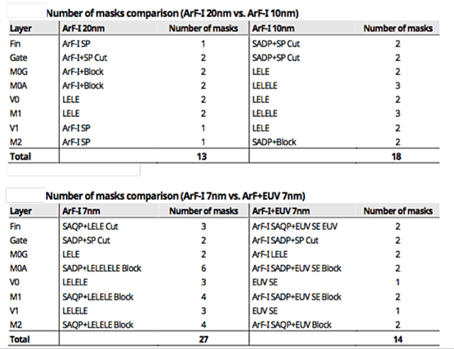
Together with self-aligned multi-patterning (SAMP) techniques like self-aligned double patterning (SADP), self-aligned quadruple patterning (SAQP), and self-aligned litho-etch-litho-etch (SALELE), these alternative approaches provide SMIC with a range of options to navigate the complexities of advanced semiconductor manufacturing, ultimately shaping the future of Chinese advanced chip fabrication.
The Future of Nanoimprint Lithography: High-Volume Production Possibilities
Nanoimprint lithography (NIL) offers potential for high-volume production with sub-10 nm resolution, revolutionizing semiconductor manufacturing. TEL and Canon have showcased NIL's sub-10 nm capabilities, making it suitable for multiple memory generations using a single mask. Challenges like edge placement errors (EPE) are addressed through precision techniques like Quasi-Atomic Layer Etch (Quasi-ALE). To achieve aggressive scaling targets, overlay accuracy and critical dimension uniformity (CDU) management are vital. NIL's simplicity and cost-effectiveness make it a promising contender, with ongoing development poised to refine its integration into semiconductor fabrication.Future Outlook for SMIC and China
193i Lithography Takes Center Stage...Again (semiengineering.com)
Does SMIC have 7nm and if so, what does it mean - SemiWiki
Look Inside Huawei Mate 60 Pro Phone Powered by Made-in-China Chip - Bloomberg
Applied Materials: SMIC Move To 7nm Node Capability Another Headwind (NASDAQ:AMAT) | Seeking Alpha


%20(1).png)

