Showing posts with label 7nm. Show all posts

Tuesday, August 30, 2022

Comparison confirms that SMIC reaches 7nm without access to western equipment & technologies

Similarities with TSMC 7nm have been found

After TechInsights revealed their initial findings on the SMIC MinerVa Bitcoin mining processor, their team did further analysis and comparison against TSMC 7nm. This new analysis confirms that despite current sanctions restricting access to the most advanced equipment technologies, Chinese Semiconductor Manufacturing International Corporation (SMIC) has used 7nm technology to manufacture the MinerVa Bitcoin Miner application-specific integrated circuit (ASIC).

The TechInsights analysis also uncovered many similarities between the SMIC 7nm and the TSMC 7nm, which are available in our comparison brief.


According to the SeekingAlpha assessment earlier this year (Applied Materials: SMIC Move To 7nm Node Capability Another Headwind (NASDAQ:AMAT) | Seeking Alpha) SMIC is using a large amount of multiple pattering mask layers like in the first TSMC and Samsung 7 nm nodes (N7). 

"At 7nm, normally 15 DUV systems and 5 EUV systems are demanded, depending on chip type and company. However, since SMIC is not permitted to use EUV, then they will be substituted by DUV, and 20 DUV systems will be used.

In both cases, multiple patterning is done to delineate that pattern, whether it is 28nm or 7nm. This multiple patterning process is more or less a trick to reach even the 28nm dimensions. The multiple patterning is typically a combination of deposition, etch, and lithography steps.

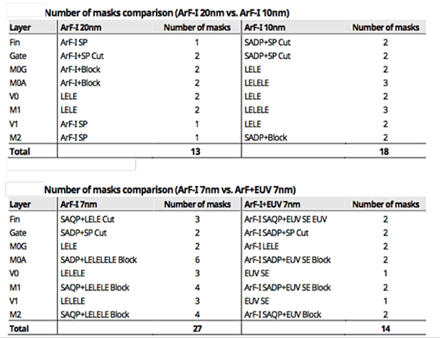
If we look at Chart 3 below, using immersion DUV (ArF-1) at the 20nm node there are 13 mask layers, each of which uses multiple dep-etch steps. If we move across the top of the chart, at 10nm there are 18 mask layers, an increase of 50% in the use of deposition-etch steps.

Multiple patterning at the 7nm node, as shown in the bottom left of the chart, requires 27 mask layers. However, by switching to EUV (bottom right) at 7nm, only 14 mask layers are required, similar to the 20nm node with DUV.

The terminology is as follows in switching from DUV to EUV:Double litho, double etch (LELE) process will be eliminated

While ArF-I would continue to be used for the self-aligned double patterning (SADP) and
Self-aligned quadruple patterning (SAQP) processes."
 

Table from SeekingAlpha as cited above

From an ALD point of view, the FEOL and metallization up to M2 use 19 in the case of Immersion Lithography (N7) vs 10 in the case of EUV (N7+) ALD spacer-defined multiple patterning masks (SADP or SAQP). However, the bigger difference is in etch for LELE etc., where EUV N7+ uses only 2 such masks.


Sunday, May 12, 2019

Intel 2019 Investor Meeting: 7 nm Product in 2021

Intel held its 2019 investor meeting May 8, 2019 (LINK), it's first since 2017, and CEO Bob Swan announced that Intel would launch its 7 nm process in 2021 to challenge TSMC's 5 nm products.

Intel's Xe graphics will be the leading 7 nm product, which will come on the heels of Intel's first discrete 10 nm GPU that arrives in 2020. The company also unveiled its first block diagram of the Ice Lake architecture and announced that its new 10nm Tiger Lake processors will come to market in 2020.
Source: Tom´s Hardware LINK

 (intel.com)

----------
By Abhishekkumar Thakur

Wednesday, January 2, 2019

IEDM 2018 Imec on Interconnect Metals Beyond Copper

At IEDM in December 2018 Imec presented recent results from their interconnect program “Interconnect metals beyond copper – reliability challenges and opportunities”, which was recently covered by Scotten Jones (SemiWiki).
 

The electrical current in interconnect lines haven’t scaled down as fast as the lines' cross sectional area, which has enhanced the current density in the lines. Initial wide aluminum (Al) interconnects were first replaced by narrower aluminum-copper (AlCu) alloys and eventually by Cu to reduce the interconnects line resistance. Now even Cu needs to be replaced by alternate materials for the narrowest lines due to the following limits:

  • Higher resistivity with shrinking line width – below 20nm exponential increase in line resistance.
  • Via resistance also goes up strongly due to the liner.
  • Thinner lines see more grains from electroplating – around 10nm line can’t meet electromigration.
Imec commenced their work on alternative materials for M0 and M1 interconnects by screening based on the two metrics—resistivity multiplied by electron mean free path and melting point. The work reflects Rhodium and Iridium as the best candidate materials for the lowest interconnects that can be reasonably integrated. Ruthenium (Ru) and Cobalt (Co) exhibit similar performance. These materials can be deposited using ALD, CVD or electroplating. Co needs a thin adhesion layer but not a barrier layer. Ru also doesn’t require any seed or barrier layer. Imec is still working on reliability tests of these materials.

Meanwhile, TSMC has been using Co capping on Cu interconnects since 16 nm due to improved electromigration. Co (TSMC) and Ru (Intel) seed layers were introduced. Intel has introduced Co contacts at 10 nm and TSMC at 7 nm. Intel has also introduced Co interconnects for metals 0 and 1 at 10 nm.

Source: SemiWiki, Scotten Jones : LINK
 
----------
By Abhishekkumar Thakur

Monday, October 29, 2018

Coventor - N7 FinFET Self-Aligned Quadruple Patterning Modeling

Coventor just released a white paper for ther modelling on FinFET Self-Aligned Quadruple Patterning for the 7nm node (N7).

You can request the paper for download here: LINK

White Paper : N7 FinFET Self-Aligned Quadruple Patterning Modeling

In this paper, we model fin pitch walk based on a process flow simulation using the Coventor SEMulator3D virtual platform. A taper angle of the fin core is introduced into the model to provide good agreement with silicon data. The impact on various Self-Aligned Quadruple Patterning process steps is assessed. Etch sensitivity to pattern density is reproduced in the model and provides insight on the effect of fin height variability.