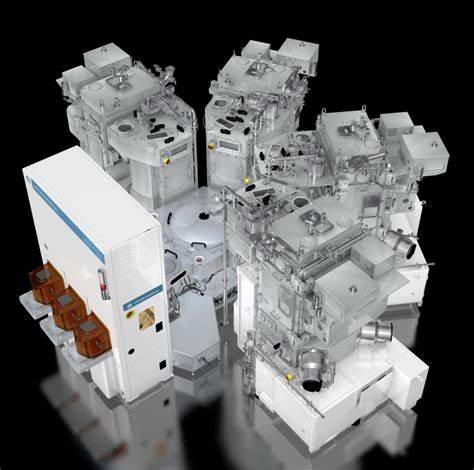
Applied Materials’ pattern-shaping technology is a breakthrough innovation that brings new capabilities to the patterning engineer's toolkit. This animation shows how engineers can replace EUV double patterning steps with the Centura® Sculpta® patterning system to reduce the cost, complexity and environmental impact of leading-edge chipmaking.
Applied Materials showcased a patterning technology that helped chipmakers to create high-performance transistors and interconnect wiring with fewer EUV lithography steps, thereby lowering the cost, complexity, and environmental impact of advanced chipmaking. To help chipmakers shrink designs without the added cost, complexity, and energy and materials consumption of EUV double patterning, Applied Materials worked closely with leading customers to develop the Centura Sculpta patterning system.
Chipmakers such as Intel, Samsung and TSMC, can now print a single EUV pattern and then use the Sculpta system to elongate the shapes in any chosen direction to reduce the space between features and increase pattern density. The Sculpta system can provide chipmakers with capital cost savings of $250 million per 100K wafer starts per month of production capacity, manufacturing cost savings of $50 per wafer, and energy savings of more than 15 kWh per wafer, the company said.
Ryan Russell, corporate vice president for logic technology development at Intel Corp, said, "Having collaborated closely with Applied Materials in the optimization of Sculpta around our process architecture, Intel will be deploying pattern-shaping capabilities to help us deliver reduced design and manufacturing costs, process cycle times and environmental impact."
Applied Materials Centura with four Sculpta chambers
Applied Materials also launched a new eBeam metrology system specifically designed to precisely measure the critical dimensions of semiconductor device features patterned with EUV and emerging High-NA EUV lithography. Applied's new VeritySEM 10 system features a unique architecture that enables low-landing energy at 2X better resolution than conventional CD-SEMs. It also provides a 30% faster scan rate to reduce interaction with the photoresist and increase throughput.
- Directed ribbon-beam capability for novel etching applications
Journal of Vacuum Science & Technology B 33, 06FA02 (2015); https://doi.org/10.1116/1.4932161


%20(1).png)

