Showing posts with label Applied Materials. Show all posts

Tuesday, February 27, 2024

Applied Materials Unveils Cutting-Edge Patterning Technologies for Next-Gen Semiconductor Device Manufacturing

Applied Materials is leading the charge into the angstrom era of chipmaking, unveiling a suite of innovative solutions at the SPIE Advanced Lithography + Patterning conference. The company's focus is on overcoming the challenges posed by extreme ultraviolet (EUV) and high-NA EUV lithography, crucial for the production of chips at 2nm process nodes and below. Their approach integrates new materials engineering, metrology techniques, and pattern-shaping technology to enhance chip performance and yield.


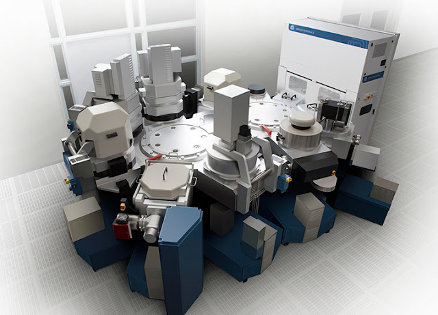
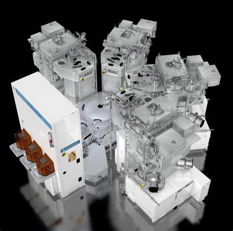
To help overcome patterning challenges for leading-edge chips, Applied Materials offers a portfolio of technologies designed to complement the latest advances in lithography. The company’s newest innovations include the Producer® XP Pioneer® CVD patterning film, the Sym3® Y Magnum™ etch system, the Centura® Sculpta® pattern-shaping system and Aselta contour technology for design-based metrology.

Central to Applied Materials' advancements is the Sculpta® pattern-shaping technology, first introduced at the previous year's conference. Sculpta has seen growing adoption among top logic chipmakers for its ability to refine EUV patterning, notably reducing double patterning steps and mitigating defects such as bridge defects. This technology not only lowers patterning costs but also improves chip yields, showcasing its increasing importance in the semiconductor manufacturing landscape.


Over the next few years, chipmakers will be looking to create “angstrom era” chips that will use EUV and High-NA EUV lithography to pattern their smallest features. An entire ecosystem of capabilities will be required to enable this advanced patterning – including software and design tools, innovations in deposition and etch, advanced metrology and inspection systems, and entirely new approaches such as pattern shaping.

In response to the issue of EUV line edge roughness, Applied Materials has launched the Sym3® Y Magnum™ etch system. This innovative system employs a combination of deposition and etch processes within a single chamber to smooth out rough edges before etching, thereby enhancing yield and chip performance.

Additionally, the company introduced the Producer® XP Pioneer® CVD patterning film, designed for high-fidelity pattern transfer with enhanced resistance to etch chemistries. This film is especially significant for advanced process nodes, offering improved sidewall feature uniformity and co-optimization with both Sculpta and the Sym3 Y Magnum system for superior patterning capabilities.

To address the critical issue of feature alignment across chip layers, Applied Materials has acquired Aselta Nanographics, integrating its design-based metrology with Applied's leading eBeam systems. This integration enables a comprehensive metrology solution that significantly enhances feature placement accuracy, crucial for optimizing chip performance and yield.

Applied Materials' expansion of its patterning solutions portfolio underscores its commitment to advancing semiconductor technology. By addressing key challenges in EUV lithography and introducing groundbreaking technologies, the company is setting new standards for the industry, driving forward the capabilities of angstrom era chipmaking.

Source: Applied Materials Expands Patterning Solutions Portfolio for Angstrom Era Chipmaking | Applied Materials

Saturday, January 20, 2024

Unveiling the Future of Material Science: Key Takeaways from the MLD and ALD Webinar

In the dynamic world of material science, the recent Applied Materials Picosun webinar held on January 16, 2024 centered on Atomic Layer Deposition (ALD) and Molecular Layer Deposition (MLD), offered a deep dive into these groundbreaking technologies and their applications in crafting advanced functional properties. 

LINK to recording: Atomic layer deposition (ALD) and molecular layer deposition (MLD) together present an elegant technique for the deposition of novel inorganic-organic materials. (picosun.com)

The webinar was given by Topias Jussila, Doctoral Researcher, Aalto University, Finland. Let's explore how ALD and MLD are shaping the future of materials at the nanoscale.

The Emergence of MLD

Molecular Layer Deposition, though a relative newcomer compared to ALD, has quickly garnered attention for its unique capabilities. MLD, which operates on the principle of sequential molecular layering, offers a versatile platform for creating hybrid materials with tailored properties. The webinar expertly delineated the different types of MLD, such as metal-aliphatics, metal-aromatics, and inorganic-organic multilayers, each presenting its distinct advantages in material fabrication.


Synergy of ALD and MLD

The fusion of ALD with MLD emerged as a focal point of discussion. This combination enhances the material properties, allowing for precise control at the nanoscale. The synergy of ALD and MLD opens doors to innovative applications, particularly in microelectronics and nanotechnology, by creating materials with unprecedented electrical, optical, and mechanical properties.


Applications That Reshape Industries

The practical applications of MLD and ALD-MLD are vast and varied. Key areas include:

Flexible Barrier Layers: MLD is particularly effective in creating ultra-thin, flexible barrier layers that are impermeable to gases and moisture. This is crucial for applications like organic light-emitting diode (OLED) displays and flexible electronics, where moisture and oxygen can degrade the performance of the devices.

Encapsulation: MLD provides an excellent method for encapsulating sensitive components, protecting them from environmental factors without compromising their functionality.

Photocatalysis: MLD materials are used in photocatalysis applications, which are important in environmental remediation and energy conversion technologies.

Electronics and Semiconductors: The combination of MLD with ALD is particularly advantageous in the electronics and semiconductor industries. It enables the precise deposition of thin films with tailored electrical and optical properties, crucial for advanced microelectronics and photonics.

Biomedical Applications: The versatility of MLD and ALD-MLD coatings also finds applications in the biomedical field, such as in drug delivery systems and bioimaging, where biocompatibility and controlled interactions with biological environments are essential.

Industrialization and Future Outlook

As for the industrialization of MLD, it is a relatively newer field compared to ALD. While ALD has been widely industrialized, particularly in the semiconductor industry, MLD is still primarily in the research and development stage, with growing interest in transitioning to industrial applications. The unique capabilities of MLD in creating organic-inorganic hybrid materials are driving research and potential industrial applications, but widespread industrial adoption might still be in progress.

Conclusion

The ALD and MLD webinar served as a beacon of knowledge, shedding light on the latest advancements and future prospects of these technologies. As we step into an era where material science plays a critical role in technological advancements, the insights from this webinar not only educate but also inspire further exploration and innovation in the field. The future of material science, undoubtedly, holds exciting possibilities, with ALD and MLD at its forefront.


Background: Topias Jussila is a second year PhD student at the Department of Chemistry and Materials Science, Aalto University, Finland. Topias carried out his Bachelor’s degree in Chemistry at the University of Helsinki and Master’s degree in Functional Materials at Aalto University. For the past two years, Topias has worked intensively with atomic layer deposition (ALD) and molecular layer deposition (MLD) with a target to develop novel thin film materials with advanced functional properties, having the main focus in iron-based inorganic and inorganic-organic materials. In addition to deposition process development, he has employed a wide range of thin film characterization methods to study the composition, structure, and functional properties of the thin films.

Wednesday, December 13, 2023

Breakthrough in Digital Lithography by Applied Materials and Ushio Boosts AI Computing Power

Ushio, Inc. have announced a significant strategic partnership, marking a new era in digital lithography technology. This collaboration aims to spearhead the transition to heterogeneous chiplet integration on large substrates like glass, a move crucial for advancing Artificial Intelligence (AI) computing capabilities.


This new digital lithography system, pioneered by Applied Materials and Ushio, is tailor-made for patterning advanced substrates vital in the AI era. With the growing demand for AI workloads, there's an increased need for larger, more functional chips. Traditional methods can't keep up with AI's performance requirements, hence the shift to heterogeneous integration (HI) techniques. These involve combining multiple chiplets in an advanced package, offering performance and bandwidth comparable to monolithic chips.


The partnership leverages Applied Materials' expertise in large substrate processing and Ushio's experience in lithography for packaging. Dr. Sundar Ramamurthy from Applied Materials highlights the new Digital Lithography Technology (DLT) as a game-changer for customers' advanced substrate roadmaps. William F. Mackenzie of Ushio emphasizes their long-standing experience in lithography systems and their commitment to this new venture.

The DLT system stands out as the only technology capable of achieving the necessary resolution for advanced substrate applications while maintaining high-volume production throughput. It can pattern line widths less than 2-microns, allowing unprecedented area density for chiplet architectures on various substrates, including glass.

Applied Materials is responsible for R&D and creating a scalable roadmap for the DLT system, aiming to push innovation in advanced packaging to 1-micron line widths and beyond. Ushio will use its established manufacturing and customer infrastructure to facilitate the technology's adoption.

While this announcement is forward-looking and subject to the usual risks and uncertainties of the tech industry, it heralds a new chapter in computing technology, potentially transforming the landscape of high-performance computing in the AI era.

- Applied Materials, Inc. is a leader in materials engineering solutions, essential in producing new chips and advanced displays worldwide.

- Ushio, Inc., established in 1964, specializes in manufacturing and selling various light sources and optical equipment, with a significant presence in industrial processes and visual imaging.

For more information or media inquiries, contact Ricky Gradwohl for Applied Materials and the Corporate Communication Department for Ushio. 

Photos and more details are available on here Breakthrough Digital Lithography Technology From Applied Materials and Ushio to Enable More Powerful Computing Systems for the AI Era | Applied Materials.

Thursday, December 7, 2023

Applied Materials and CEA-Leti Forge New Joint Lab to Spearhead Specialty Chip Market Innovations

Applied Materials and CEA-Leti have announced a significant expansion of their collaboration, focusing on innovative materials engineering solutions tailored for specialty semiconductor markets. The joint lab, situated at CEA-Leti, is dedicated to propelling semiconductor device development, particularly for Applied Materials' ICAPS (IoT, Communications, Automotive, Power, and Sensors) customers.

This partnership underscores a growing demand in the ICAPS sector, fueled by advancements in industrial automation, IoT, electric vehicles, and green energy initiatives. The joint lab will tackle various materials engineering challenges to facilitate the next generation of ICAPS device innovations. Equipped with Applied Materials' advanced 200mm and 300mm wafer processing systems, the lab leverages CEA-Leti's expertise in new materials evaluation and device validation.


The joint lab features several of Applied Materials’ 200mm and 300mm wafer processing systems, such as this Endura® system, and leverages CEA-Leti’s world-class capabilities for evaluating performance of new materials and device validation.​

The collaboration aims to enhance power efficiency, performance, and cost-effectiveness, while also reducing time to market. Aninda Moitra, corporate vice president and general manager of Applied Materials' ICAPS business, emphasizes this initiative as an extension of a decade-long successful partnership, geared towards accelerating innovation in specialty semiconductor technologies.

Sébastian Dauvé, CEO of CEA-Leti, reflects on the decade of collaborative projects leading up to this new joint lab. These projects spanned advanced metrology, memory materials, optical devices, bonding techniques, and chemical-mechanical planarization. The results have consistently delivered high value, setting a solid foundation for this expanded engagement.

The lab not only aims to develop unique technological solutions for Applied Materials' customers but also supports CEA-Leti's internal R&D programs, overcoming current technical challenges. This initiative marks a significant step in the collaboration, promising to bring breakthroughs in specialty semiconductor technology to global markets.

Friday, September 22, 2023

ASML's 2023 Outlook: Surging Ahead in Semiconductor Equipment Despite Challenges and Export Controls

In 2023, ASML, the leading semiconductor lithography equipment supplier, is set to achieve remarkable success, outpacing its rivals and emerging as the number 1 provider of Wafer Fabrication Equipment. Boasting an impressive 30% revenue growth forecast for the year, ASML is thriving amidst an industry landscape marked by its consistent performance. With a substantial backlog of cutting-edge Deep Ultraviolet (DUV) and Extreme Ultraviolet (EUV) systems and surging demand from China, ASML's growth continues despite hurdles like supply chain disruptions and regulatory changes, ASML remains a beacon of innovation and resilience in the semiconductor sector.

By Abhishek Kumar Thakur and Jonas Sundqvist

ASML, a leading supplier of semiconductor equipment, is poised for a significant year in 2023, projected to surpass Applied Materials (AMAT) as the top provider of Wafer Fabrication Equipment. This achievement is attributed to ASML's robust revenue growth, expected to reach a remarkable 30% increase in 2023, while Applied Materials faces a decline of 20% according to Seeking Alpha*. ASML's success can be attributed to a substantial backlog of Deep Ultraviolet (DUV) and Extreme Ultraviolet (EUV) systems, driven by heightened demand in China.

* Fact check: Due to strong DUV revenue and despite the increased uncertainties, ASML expects strong growth for 2023 with a net sales increase towards 30% and a slight improvement in gross margin, relative to 2022. ASML Holding revenue for the twelve months ending June 30, 2023 was $27.293B, a 25.97% increase year-over-year. AMAT revenue is estimated to increase by 2.6% to 26.33 B. Meaning ASML would pass bu end of 2023.

https://finance.yahoo.com/quote/AMAT/analysis/ 


Despite facing challenges like supply chain disruptions and a factory fire, ASML has consistently ranked among the top three semiconductor equipment suppliers since 2017. Their backlog of EUV systems, combined with growing acceptance of DUV tools, contributes to their strong performance.

However, potential headwinds include supply chain concerns, past issues like the Berlin factory fire, and looming sanctions affecting exports to China. While ASML has addressed some challenges, the possibility of US sanctions in 2024 poses a threat to its growth.

Furthermore, ASML now faces new export controls imposed by the Netherlands, impacting shipments to China. While the company downplays these controls' immediate financial impact, they are expected to affect specific DUV systems, adding to global efforts to limit China's semiconductor advancements.

In this volatile landscape, ASML's ability to adapt to evolving regulations and maintain its technological leadership will be crucial. The impact of these restrictions, especially on shipments to China, could influence the company's growth trajectory in the semiconductor industry. Despite these challenges, ASML remains a prominent player with significant potential in the semiconductor equipment market.

ASML is set to deliver the industry's first High-NA extreme ultraviolet (EUV) lithography scanner by the end of 2023, marking a significant development for advanced chip manufacturing. The Twinscan EXE:5000 pilot scanner with a 0.55 numerical aperture (NA) will enable chipmakers to explore High-NA EUV technology. This innovation is crucial for achieving an 8nm resolution, suitable for manufacturing technologies beyond 5nm nodes. Intel is expected to be the first customer, but integration and adoption details are still uncertain. This advancement requires substantial investments, with reports suggesting costs of $300-400 million per unit.

To add some colour, initially, Intel had plans to employ ASML's High-NA tools for its 18A (1.8 nm) production node, scheduled for high-volume manufacturing in 2025, aligning with ASML's Twinscan EXE:5200 delivery. However, Intel accelerated its 18A production, moving it to the latter part of 2024. This change in strategy involved the use of ASML's Twinscan NXE:3600D/3800E with two exposures and Applied Material's Endura Sculpta pattern-shaping system. The objective was to reduce reliance on EUV double patterning techniques. Applied Materials' Centura Sculpta is a pattern-shaping machine equipped with a unique algorithm that can manipulate patterns produced by an EUV scanner. It has the capability to stretch these patterns in a user-defined direction along the X-axis. This process effectively reduces the space between features and enhances pattern density. This means that moving ahead ASML and Applied Materials are entering an interesting competitive space previously not encountered.

ASMLs Products

As an background, ASML specializes in the production of cutting-edge lithography systems crucial for semiconductor manufacturing. Their product portfolio includes the following key offerings:

Extreme Ultraviolet (EUV) Lithography Machines: ASML's EUV lithography machines are at the forefront of semiconductor manufacturing technology. These machines use extremely short wavelengths of light to create intricate patterns on silicon wafers, enabling the production of advanced and smaller semiconductor chips. EUV technology is essential for next-generation processors and memory chips.

Deep Ultraviolet (DUV) Lithography Machines: DUV lithography systems are another vital component of ASML's product lineup. They use longer wavelengths of light compared to EUV and are employed for a wide range of semiconductor applications, including memory and logic chip production. ASML's DUV systems are known for their precision and reliability.

TWINSCAN Series: Within the DUV lithography category, ASML offers the TWINSCAN series, which includes machines like the TWINSCAN NXT:2000i, NXT:2050i, and NXT:2100i. These systems are designed for immersion lithography, where the wafer and the lens are submerged in a liquid, enhancing precision and resolution.

EUV High Numerical Aperture (NA) Systems: ASML has been advancing its lithography machines by increasing the numerical aperture (NA), a key parameter that affects resolution. High-NA systems are capable of printing even smaller features on semiconductor wafers, enabling the production of highly advanced chips.

ASML's lithography machines are considered critical infrastructure for semiconductor manufacturing, and the company's technological leadership in this area has positioned it as a dominant player in the industry. The company's ability to innovate and adapt its lithography systems to meet the ever-increasing demands of semiconductor manufacturers has been a key factor in its success and growth prospects. However, the recent export controls and geopolitical pressures, particularly concerning shipments to China, introduce additional challenges and uncertainties for ASML and its specialized products.

Sources:

ASML Hit With New Dutch Limits on Chip Gear Exports to China - Bloomberg

ASML To Top WFE Semiconductor Equipment In 2023, Topping Applied Materials | Seeking Alpha

ASML to ship first pilot tool in its next product line in 2023, CEO says | Reuters

ASML to Deliver First High-NA EUV Tool This Year (anandtech.com)

EUV Alternative Speeds Up Chip Production - EE Times

BALD Engineering - Born in Finland, Born to ALD: ASML Remains on Track to Deliver High NA EUV Machines in 2023

BALD Engineering - Born in Finland, Born to ALD: Netherlands' chip tool export controls take effect for DUV Lithography and ALD

BALD Engineering - Born in Finland, Born to ALD: Applied Materials’ Pattern-Shaping Technology - Centura Sculpta


Saturday, September 9, 2023

SkyWater Installs Advanced Atomic Layer Deposition System from Picosun

SkyWater Technology (SkyWater Technology | U.S. Semiconductor Manufacturer) has announced the installation of an Atomic Layer Deposition (ALD) system, the Applied Picosun MorpherTM, to offer advanced semiconductor processing capabilities to its customers. ALD is a precise method for depositing ultra-thin, uniform, and conformal material layers, making it ideal for applications like sensors and emerging memory technologies. SkyWater's Technology as a Service (TaaS) model allows customers to access this technology for developing and producing innovative technologies. The ALD tool has two thermal batch chambers for depositing metals and oxides, ensuring high-quality and repeatable results. This move aims to meet the increasing demand for ALD applications in semiconductor processing, particularly in areas such as biosensors, photonics, and extreme CMOS applications.


SkyWater Minnesota Fab (SkyWater)

SkyWater Technology is a leading U.S.-based semiconductor manufacturer with a unique Technology as a Service (TaaS) model. They offer a wide range of semiconductor solutions, serve various industries, and emphasize innovation and quality. Their expertise spans diverse semiconductor categories, from mixed-signal CMOS to photonics, and they are accredited as a Category 1A Trusted Foundry by the Defense Microelectronics Activity (DMEA).


The Morpher ALD tool is designed for precise and controlled deposition of thin material layers, making it suitable for various semiconductor applications. It is configured with two thermal batch chambers, one for depositing metals and another for depositing oxides, allowing for flexibility and efficiency in semiconductor fabrication processes. This tool is being installed at SkyWater Technology to provide their customers with access to ALD capabilities for developing and producing advanced semiconductor technologies.


Tuesday, September 5, 2023

Revolutionizing Pharmaceutical Packaging and Labware: ALD Technology Enhances Material Properties

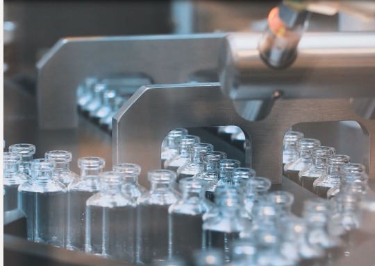
Picosun, an Applied Materials company, is proud to announce a breakthrough in enhancing the properties of packaging materials and labware using Atomic Layer Deposition (ALD) technology. ALD offers impermeable barriers and functional surfaces, revolutionizing pharmaceutical packaging and labware for the better.

Date: 12th December Time: 3:00 PM London / 10:00 AM New York

As pharmaceutical packaging evolves to accommodate biological drugs and novel packaging solutions, ALD technology steps in to provide ultra-thin, uniform, and precise material layers with atomic-level thickness and composition. This innovation caters to the demands of primary packaging materials and labware, offering impermeable barriers against leachables and ensuring biocompatibility.

Join us for an insightful webinar to explore how ALD can elevate the performance of packaging materials and labware. Stay ahead in the world of pharmaceutical and medical advancements!

Register now to secure your spot and gain valuable insights. Stay at the forefront of innovation with Picosun and ALD.


Tuesday, August 22, 2023

Applied Materials Surges on Impressive Q3 Earnings and Bullish Guidance

Applied Materials Inc. (NASDAQ: AMAT) witnessed a robust surge of nearly 4% in after-hours trading following the release of its third-quarter financial results that significantly outperformed expectations. The semiconductor capital equipment manufacturer reported adjusted earnings of $1.90 per share on $6.43 billion in revenue for the quarter ending July 30. 

Notably, the company's strategic focus on foundry and logic revenue paid off, accounting for 79% of quarterly sales compared to 66% in the prior year's quarter. Additionally, Applied Materials generated a substantial $2.58 billion in cash from operations during this period. The company's bullish performance extended to its outlook, with fourth-quarter net sales projected at approximately $6.51 billion, accompanied by adjusted earnings per share ranging from $1.82 to $2.18. These figures comfortably exceeded analyst estimates, highlighting Applied Materials' robust position in the semiconductor industry.


Applied Materials, Inc. (AMAT) Q3 2023 Earnings Call TranscriptSA TranscriptsThu, Aug. 17

Applied Materials, Inc. 2023 Q3 - Results - Earnings Call PresentationSA TranscriptsThu, Aug. 17

Friday, March 3, 2023

Applied Materials’ Pattern-Shaping Technology - Centura Sculpta

Applied Materials’ pattern-shaping technology is a breakthrough innovation that brings new capabilities to the patterning engineer's toolkit. This animation shows how engineers can replace EUV double patterning steps with the Centura® Sculpta® patterning system to reduce the cost, complexity and environmental impact of leading-edge chipmaking.


Applied Materials showcased a patterning technology that helped chipmakers to create high-performance transistors and interconnect wiring with fewer EUV lithography steps, thereby lowering the cost, complexity, and environmental impact of advanced chipmaking. To help chipmakers shrink designs without the added cost, complexity, and energy and materials consumption of EUV double patterning, Applied Materials worked closely with leading customers to develop the Centura Sculpta patterning system.

Chipmakers such as Intel, Samsung and TSMC, can now print a single EUV pattern and then use the Sculpta system to elongate the shapes in any chosen direction to reduce the space between features and increase pattern density. The Sculpta system can provide chipmakers with capital cost savings of $250 million per 100K wafer starts per month of production capacity, manufacturing cost savings of $50 per wafer, and energy savings of more than 15 kWh per wafer, the company said.

Ryan Russell, corporate vice president for logic technology development at Intel Corp, said, "Having collaborated closely with Applied Materials in the optimization of Sculpta around our process architecture, Intel will be deploying pattern-shaping capabilities to help us deliver reduced design and manufacturing costs, process cycle times and environmental impact."


Applied Materials Centura with four Sculpta chambers

Applied Materials also launched a new eBeam metrology system specifically designed to precisely measure the critical dimensions of semiconductor device features patterned with EUV and emerging High-NA EUV lithography. Applied's new VeritySEM 10 system features a unique architecture that enables low-landing energy at 2X better resolution than conventional CD-SEMs. It also provides a 30% faster scan rate to reduce interaction with the photoresist and increase throughput​.
Journal of Vacuum Science & Technology B 33, 06FA02 (2015); https://doi.org/10.1116/1.4932161


Friday, December 23, 2022

Picosun initiates R&D program in Finland for sustainable semiconductor manufacturing

ESPOO, Finland, 22nd of December 2022 – Picosun, an Applied Materials company, has received funding from Business Finland to form an R&D program in the country focused on reducing the environmental impact of semiconductor manufacturing.

The four-year program, called “Chip Zero,” seeks to bring together companies across the semiconductor ecosystem in Finland with a shared mission of developing chips with zero lifetime emissions by reducing the carbon footprint of chip manufacturing and increasing the efficiency of semiconductor decarbonization applications. Picosun will initiate and lead the program with a significant grant from Business Finland. The aim is to scale the program over time with contributions from ecosystem partners to reach more than 100M€ in R&D investments.


Photo, Björn Engström, Oravais, Ostrobothnia, Finland.

Chip Zero will include efforts to reduce energy consumption and the environmental impact of chemical use in semiconductor manufacturing. Specific goals include achieving a 50-percent reduction in energy and chemical consumption of thin-film deposition and a double-digit increase in the efficiency of power electronic component applications, such as electric vehicle (EV) chargers and electric motor control electronics, by 2030. Among the strategies to achieve these goals is the development of optimized process flows for chip manufacturing.

“Picosun is excited to lead the Chip Zero program and bring together Finland’s strong technology R&D ecosystem with a common objective of developing more efficient chips and minimizing the environmental impact of manufacturing. We look forward to collaborating across the value chain to drive critical advances that will accelerate a greener and more sustainable semiconductor industry in Finland,” says Dr. Jani Kivioja, CTO of Picosun.

“With the global semiconductor market projected to reach US$1 trillion by 2030*, the need for greater efficiency in chip manufacturing is more important than ever. Finland has significant and pioneering competences in key chipmaking technologies, and the Chip Zero program intends to focus these capabilities on strengthening the country’s sustainability efforts,” continues Jussi Rautee, CEO of Picosun and Vice President of Applied Materials.

“The opportunity for technology to shape a more sustainable world has never been more promising,” says Chris Librie, Applied Materials Director of ESG, Corporate Sustainability and Reporting. “At Applied Materials, our vision is to Make Possible a Better Future, and we are pleased that our team in Finland is making a positive difference through programs like Chip Zero that aim to reduce the environmental impact of computing.”


Friday, November 25, 2022

Applied Materials Delivers Strong FY 2022 Numbers including Picosun ALD

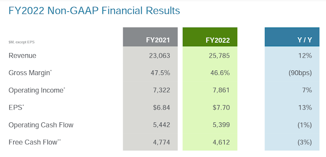
Semiconductor equipment maker Applied Materials has reported strong earnings for FY 2022 (ended October 30). Total sales revenue increased 12% YoY to $25.78 billion despite supply chain shortages, geopolitical and macroeconomic headwinds, and softening consumer demand.

LINK: https://ir.appliedmaterials.com/

The company’s uniquely enabling technology and growing installed base will be its key growth drivers as chipmakers accelerate ramping up of new process nodes in R&D for high-volume manufacturing.


Key developments in FY 2022
  • Applied Materials acquired Picosun, a Finland-based innovator in atomic layer deposition (ALD) technology. This acquisition broadens Applied’s product portfolio and puts it in a great position to capture a large portion of the specialty semiconductor market in the coming years.
  • Collaboration with the Institute of Microelectronics (IME), a research institute under Singapore’s Agency for Science, Technology and Research (A*STAR). IME’s strategic R&D capabilities complement well Applied’s expertise in advanced packaging solutions and will accelerate material, equipment and process technology solutions for hybrid bonding and other emerging, 3D chip integration technologies.
  • Introduced new Ioniq™ PVD system to solve wiring resistance challenges of 2D scaling. This new integrated solution offers a significant reduction in electrical resistance, which has become a critical bottleneck to further improvements in chip performance and power.
Financial highlights
  • Semiconductor Systems revenue increased 15% YoY in FY 2022 to $18,797 million on account of strong orders as customers continued to invest in next-generation technology.
  • Applied Materials’ service revenue increased 11% YoY in FY 2022 to $5,543 million, accounting for 21% of the annual net revenue.
  • Display and Adjacent Markets revenue decreased 19% YoY in FY 2022 to $ 1,331 million.
  • Non-GAAP gross margin was at 46.6% in FY 2022.
  • Non-GAAP operating profit grew by over 7% to $7.86 billion.
  • Non-GAAP EPS increased nearly 13% to $7.70.
  • Total ending backlog increased 62% to $19 billion with Semiconductor Systems backlog increasing 90% to nearly $12.7 billion and services backlog increasing 30% to over $5.6 billion.
  • The company generated about $5.4 billion in operating cash flow and over $4.6 billion in free cash flow.
  • The company’s installed base grew 8% YoY in FY 2022.
  • The number of tools under comprehensive, long-term service contracts grew 16% YoY with the over 90% renewal rate for these agreements demonstrating the value customers see in subscription services.
  • New export regulations for US semiconductor technology sold in China reduced Semiconductor Systems and AGS fourth quarter revenue by approximately $280 million.

Thursday, June 16, 2022

Applied Materials Broadens its Technology Portfolio for Specialty Chips with Acquisition of Picosun

SANTA CLARA, Calif., June 16, 2022 – Applied Materials, Inc. today announced it has acquired Picosun Oy, a privately held semiconductor equipment company based in Espoo, Finland. Picosun is an innovator in atomic layer deposition (ALD) technology, primarily for specialty semiconductors.


As electronic products become smarter and more connected, they require greater numbers of specialty semiconductors built on non-leading-edge process nodes. Applied’s ICAPS (IoT, Communications, Automotive, Power and Sensors) group provides materials engineering solutions to customers in these growing markets. The addition of Picosun’s ALD technology broadens the Applied ICAPS product portfolio and customer engagements. Picosun also brings to Applied deep R&D capabilities, talented teams and strong relationships with leading research institutions and universities throughout the world.

“Picosun is a pioneer in ALD technology with products that serve fast-growing segments of the specialty foundry-logic market,” said Gary Dickerson, President and CEO of Applied Materials. “The addition of Picosun complements Applied Materials’ technology portfolio and expands our opportunities to accelerate our customers’ roadmaps.”

“Rapid growth in the number of connected devices is driving a tremendous need for innovation in the chips used to bridge the analog and digital worlds,” said Sundar Ramamurthy, Group Vice President and General Manager of the ICAPS group at Applied Materials. “Bringing Picosun’s talented team to Applied Materials will strengthen our ability to help customers add more intelligence and functionality to a wide variety of edge computing devices.”

“Picosun has a strong history of innovation, with roots dating back to the invention of ALD technology nearly 50 years ago,” said Kustaa Poutiainen, Former Chairman of the Board of Picosun. “As we look ahead to our next phase of growth, we believe starting a new journey as part of Applied Materials – a company we have long admired – is the best path forward and will create exciting opportunities for our employees, customers and research partners.”

The Picosun team will continue to be based in Finland and will report into Applied’s ICAPS group.

The transaction has been approved by the Ministry of Economic Affairs and Employment of Finland; no other regulatory approvals were required. Financial terms of the transaction were not disclosed.

Goldman Sachs & Co. LLC served as financial advisor and Hogan Lovells US LLP served as legal counsel for Applied Materials.

About Applied Materials

Applied Materials, Inc. (Nasdaq: AMAT) is the leader in materials engineering solutions used to produce virtually every new chip and advanced display in the world. Our expertise in modifying materials at atomic levels and on an industrial scale enables customers to transform possibilities into reality. At Applied Materials, our innovations make possible a better future. Learn more at www.appliedmaterials.com.

About Picosun

Picosun provides the most advanced ALD (Atomic Layer Deposition) thin film coating solutions for global industries. Picosun’s ALD solutions enable a technological leap into the future, with turn-key production processes and unmatched, pioneering expertise in the field – dating back to the invention of the technology itself. Today, PICOSUN® ALD equipment are in daily manufacturing use in numerous leading industries around the world. Picosun is based in Finland, with subsidiaries in Germany, USA, Singapore, Japan, South Korea, China mainland and Taiwan, offices in India and France, and a world-wide sales and support network. Visit www.picosun.com.

Saturday, June 12, 2021

Applied Materials to present New Innovations Needed to Continue Scaling Advanced Logic (June 16)

Applied Materials (Santa Clara, USA): The semiconductor industry is at a crossroads. Demand for chips has never been greater as we enter the early stages of a new wave of growth fueled by the Internet of Things, Big Data and AI. At the same time, it’s become apparent that conventional Moore’s Law 2D scaling techniques are no longer able to deliver the consistent improvements in power, performance, area-cost and time to market (PPACt) that chipmakers have long relied on. This is particularly the case for logic chips, which serve as the main processing engine in nearly every electronic product and where power efficiency and performance are critical.

To shed light on this issue, Applied Materials is hosting an online Logic Master Class on Wednesday, June 16. I will be joined by other experts from Applied and the industry to discuss the logic scaling roadmap, including challenges and solutions for delivering continued improvements in PPACt. We will be exploring several different areas, including transistor and interconnect scaling, patterning and design technology co-optimization (DTCO). The common denominator underlying all of these areas is the need to supplement classic 2D scaling with a combination of approaches that includes new chip architectures, new 3D structures, novel materials, new ways to shrink features and new ways to connect chips with advanced packaging.

Source: Applied Materials Blog (LINK)


Primary modules of a FinFET are channel and shallow trench isolation (1), high-k metal gate (2) and transistor source/drain resistance (3). (Credit: Applied Materials)

Friday, May 7, 2021

Applied Materials MEMORY MASTER CLASS 2021 - slide deck

I missed this opportunity, however, I am grateful for Lita Shon-Roy just sending me the link to the slide deck - Tack så mycket. 

Slide deck for the Memory Class LINK

Next class up is Logic June 16, 2021 followed by more interesting topics in 2nd half 2021:

  • Specialty semiconductors
  • Heterogeneous design and advanced packaging
  • Inspection and process control

Teaser slide (Credit Dr. Sony Varghese, Director of Strategic Marketing at at Applied Materials)

You are welcome to contact us at TECHCET (jsundqvist@techcet.com) to dig further into the future surge of materials to realize the data-driven economy:

  • ALD/CVD precursors
  • Metals/PVD Targets
  • Photoresist
  • Wet chemicals
  • CMP pads & slurries
  • Bulk, Rare and Speciality gases
  • Wafers

Applied Materials Introduces Materials Engineering Solutions for DRAM Scaling

  • New Draco™ hard mask material co-optimized with Sym3® Y etcher to accelerate DRAM capacitor scaling
  • DRAM makers adopting Black Diamond®, the low-k dielectric material pioneered by Applied Materials to overcome interconnect scaling challenges in logic
  • High-k metal gate transistors now being introduced in advanced DRAM designs to boost performance and reduce power while shrinking the periphery logic to improve area and cost
SANTA CLARA, Calif., May 05, 2021 (GLOBE NEWSWIRE) -- Applied Materials, Inc. today announced materials engineering solutions that give its memory customers three new ways to further scale DRAM and accelerate improvements in chip performance, power, area, cost and time to market (PPACt).
The Draco hard mask resolves this issue with a new material whose selectivity is more than 30 percent higher than conventional DRAM capacitor hard masks. It enables the deposition of a 30 percent thinner hard mask, thus decreasing the capacitor’s aspect ratio and easing the difficulty of the etch process.

The digital transformation of the global economy is generating record demand for DRAM. The Internet of Things is creating hundreds of billions of new computing devices at the edge which are driving an exponential increase in data transmitted to the cloud for processing. The industry urgently needs breakthroughs that can allow DRAM to scale to reduce area and cost while also operating at higher speeds and using less power.
Applied Materials is working with DRAM customers to commercialize three materials engineering solutions that create new ways to shrink as well as improve performance and power. The solutions target three areas of DRAM chips: storage capacitors, interconnect wiring and logic transistors. They are now ramping into high volume and are expected to significantly increase Applied’s DRAM revenue over the next several years.

Introducing Draco™ Hard Mask for Capacitor Scaling

Since over 55 percent of a DRAM chip’s die area is occupied by the memory arrays, increasing the density of these cells is the biggest lever for reducing cost per bit. Data is stored as charges in cylindrical, vertically arranged capacitors that need as much surface area as possible to hold adequate numbers of electrons. As DRAM makers narrow the capacitors, they also elongate them to maximize surface area. A new technology challenge to DRAM scaling has emerged: the etching of the deep capacitor holes threatens to exceed the limits of the “hard mask” material that acts as a stencil to determine where each cylinder is placed. If the hard mask is etched through, the pattern is ruined. Taller hard masks are not viable because as the combined depth of the hard masks and capacitor holes exceeds certain limits, etch byproducts remain and cause bending, twisting and uneven depths.


Applied Producer® XP Precision® Draco™ CVD

The solution is Draco™, a new hard mask material that has been co-optimized to work with Applied’s Sym3® Y etch system in a process monitored by Applied’s PROVision® eBeam metrology and inspection system that can take nearly half a million measurements per hour. The Draco hard mask increases etch selectivity by more than 30 percent which enables a shorter mask. Draco hard mask and Sym3 Y co-optimization includes advanced RF pulsing which synchronizes etching with byproduct removal to enable patterning holes that are perfectly cylindrical, straight and uniform. The PROVision eBeam system gives customers massive, immediate actionable data on hard mask critical dimension uniformity which is the key to capacitor uniformity. Applied’s solution provides customers with a 50-percent improvement in local critical dimension uniformity and reduces bridge defects by 100X, thus increasing yields.


Implementation of Draco for DRAM capacitors. (Applied Materials Master Memory Class May the 5th 2021 LINK)

“The best way to quickly solve materials engineering challenges with our customers is to co-optimize adjacent steps and use massive measurements and AI to optimize process variables,” said Dr. Raman Achutharaman, group vice president, Semiconductor Products Group at Applied Materials.


Bringing Black Diamond® Low-k Dielectric to the DRAM Market

A second key lever of DRAM scaling is reducing the die area needed by the interconnect wiring that routes signals to and from the memory arrays. Each of the metal lines is surrounded by an insulating dielectric material to prevent interference between data signals. For the past 25 years, DRAM makers have used one of two silicon oxides – silane and tetraethoxysilane (TEOS) – as the dielectric material. Continual thinning of the dielectric layers has reduced DRAM die sizes but created a new technology challenge: the dielectrics are now too thin to prevent capacitive coupling in the metal lines whereby signals interfere with one another causing higher power consumption, slower performance, increased heat and reliability risks.

The solution is Black Diamond®, a low-k dielectric material first used in advanced logic. With DRAM designs now experiencing similar scaling challenges, Applied is adapting Black Diamond to the DRAM market and making it available on the highly productive Producer® GT platform. Black Diamond for DRAM enables smaller, more compact interconnect wires that can move signals through the chips at multi-gigahertz speeds without interference and at lower power consumption.

High-k Metal Gate Transistors Bring PPAC Improvements to DRAM

A third key lever of DRAM scaling is improving the performance, power, area and cost of the transistors used in the periphery logic of the chip to help drive the input-output (I/O) operations needed in high-performance DRAM like those based on the new DDR5 specification.

Until today, DRAM used transistors based on polysilicon-oxide which were phased out in foundry-logic by the 28-nanometer node because extreme thinning of the gate dielectric allowed electrons to leak, thereby wasting power and limiting performance. Logic makers adopted high-k metal gate (HKMG) transistors, replacing the polysilicon with a metal gate and the dielectric with hafnium oxide, a material that improves gate capacitance, leakage and performance. Now memory makers are designing HKMG transistors into advanced DRAM designs to improve performance, power, area and cost. In DRAM as in logic, HKMG will increasingly replace polysilicon transistors over time.

This technology inflection in DRAM creates growth opportunities for Applied Materials. The more complex and delicate HKMG materials stack is challenging to manufacture, and in-vacuum processing of adjacent steps using Applied’s Endura® Avenir™ RFPVD system has become the industry’s preferred solution. HKMG transistors also benefit from Applied’s epitaxial deposition technologies such as Centura® RP Epi along with film treatments including RadOx™ RTP, Radiance® RTP and DPN which are used to fine-tune the transistor characteristics for optimum performance.

“Draco hard mask and Black Diamond low-k dielectric are being adopted by leading DRAM customers, and the first HKMG DRAMs are now being introduced,” added Dr. Achutharaman. “Applied Materials projects billions of dollars in revenue growth as these DRAM inflections play out over the next several years.”

Additional information about the growth outlook for these technologies is being provided at Applied’s 2021 Memory Master Class being held later today. For more information, please visit the investor page of our website at https://ir.appliedmaterials.com.

Thursday, April 8, 2021

Why China denied Applied Materials take over of Hitachi Kokusai

According to a recent analysis by Robert Castellano (Seeking Alpha/The Information Network LINK), Hitachi Kokusai holds a strong position in tube/non-tube LPCVD and oxidation/diffusion semiconductor equipment. For some time Applied Material has planned the acquisition of Kokusai that would have increased its global market share, for silicon wafer processing equipment by adding a big segment that it does not have in its product portfolio - LPCVD, Diffusion, and ALD Furnaces. According to the market assessment, Hitachi Kokusai holds a leading market share in this segment over No. 2. Tokyo Electron. 

Castellano brings up the interesting observation that "China blocked Applied Materials' acquisition of Kokusai while permitting the Marvell-Inphi deal the same week". Basically meaning that there are more than just US-China Trade issues behind the decision. He concludes that "China is developing a home-grown equipment industry infrastructure, and the deal would impede on that effort." and follows up by breaking up the segments and global competitive situation as below.

Summary by Castellano of China OEM active in LPCVD, Diffusion, and ALD segments vs. the global leaders

China’s NAURA makes oxidation and diffusion furnaces and its products have captured a significant share (40-50%) of YMTC’s thermal process equipment purchases, per our channel checks. In RTP, major players include Applied Materials, Tokyo Electron, and Mattson Technology.

NAURA is developing etchers and deposition equipment for 7nm and 5nm nodes. NAURA has a large product offering, and its customers consist of SMIC, Hua Hong, YMTC, and GTA Semiconductors.

NAURA also makes thermal furnaces and has a 45% share of China’s memory maker YMTC purchases. Whereas NAURA sold 8 etch systems and 6 CVD and ALD deposition systems to Chinese semiconductor companies, the company sold 34 furnaces in 2019 as well as 16 cleaning systems.

Shenyang Piotech also supplies PECVD and ALD deposition equipment. Piotech received orders for 4 PECVD (for SiN, SiO2) systems from YMTC, and is also receiving repeat orders from Hua Hong, and SMIC.


The size of the semiconductor equipment market and the small share China's equipment suppliers currently enjoy compared to foreign suppliers (source: The Information Network LINK)

Wednesday, March 24, 2021

Applied Materials may kill $3.5B buy of Japanese ALD and CVD Furnace Company Kokusai over delayed approval by China

Applied Materials Inc. on Monday said that its $3.5 billion offer to buy Kokusai Electric Corp. may be terminated because the deal hasn't been able to get timely approval from Chinese regulators. The Santa Clara chip manufacturing equipment company set a March 19 deadline on the deal late in December when it increased how much it would pay KKR HKE Investment L.P. for the Japanese company. The original price was $2.2 billion. But it said on Monday that it will likely now pay KKR a termination fee.


Trouble to reach approval in China has been foreseen by several analysts since the announcement 2019, see below for more details.

  • Kokusai is a small acquisition for Applied materials as compared to the previously failed mega-merger with Tokyo Electron
  • Kokusai, which counts Samsung, SK Hynix, Toshiba, and Micron among its top customers, reported revenue of $1.24 billion as of March 2018.
  • Kokusai’s batch wafer processing tools are less technology-intensive than Applied Materials’ single wafer tools, the recent focus on ultra-thin films has driven renewed interest in this group.
Background: 
  • Impacts of the US-China trade conflict on the semiconductor equipment market and ALD LINK
  • ASM International settles with Kokusai for Batch ALD patent licenses (US$61 million) LINK
  • Applied Materials to buy Japan's Kokusai to boost memory chip business and ALD LINK

Friday, December 18, 2020

Nanexa AB signs USD 3 million Investment Agreement with Applied Materials to scale-up GMP production site for ALD-coated pharmaceuticals

Nanexa AB (publ) today announced that the company has entered into an investment agreement with Applied Ventures, LLC, the venture capital arm of Applied Materials, Inc., whereby Applied Ventures intends to invest up to USD 3 million in Nanexa during 2021 to support continued development and expansion. USD 1 million will be invested in January 2021 and additional investments of up to USD 2 million are planned later in 2021. The investment will be made through a directed issue to Applied Ventures of a mix of shares and share warrants decided upon by Nanexa with support of the authorization of the Annual General Meeting held on June 2, 2020 (the “Directed Issue”).


As announced today in a separate press release, Nanexa and Applied Materials have entered into a joint development agreement to validate, adapt and scale up Nanexa’s production of ALD-coated injectable drugs. Simultaneously, Nanexa has entered into an investment agreement with Applied Ventures, pursuant to which Nanexa has undertaken to, as authorized by the Annual General Meeting held on June 2, 2020, resolve to issue up to a total of 4 244 770 new shares and share warrants of series 2020/2021 in Nanexa, and Applied Ventures has undertaken to subscribe for newly issued shares and share warrants. In total, Applied Ventures has committed to invest at least USD 1 million, but the Directed Issue is intended to raise around USD 3 million before transaction costs.

“We are very pleased to welcome Applied Ventures as a new industrial investor in Nanexa. Their support is a great recognition of the PharmaShell® technology and Nanexa’s future potential,” says David Westberg, CEO of Nanexa.

The Directed Issue is divided into two tranches where the first tranche amounts to an investment of USD 1 million. The subscription price for the shares of the first tranche shall equal the volume weighted average price (“VWAP”) during the period from and including December 22, 2020 until and including January 11, 2021, less five percent. The SEK investment amount in the first tranche shall be determined by the average USD/SEK exchange rate during the same measurement period.

For the second tranche Applied Ventures has the option, but not the obligation, to exercise warrants of series 2020/2021 to subscribe for up to the number of shares equal to 4 244 770 shares less the number of shares issued in the first tranche. The warrants can be exercised during two different subscription periods; 1-15 April 2021 and 1-15 December 2021. Applied Ventures will take a decision on how many warrants to exercise in each subscription period. The subscription price in the second tranche shall equal the VWAP during the ten trading days immediately preceding the respective subscription periods, less ten percent.

The maximum potential dilution from the Directed Issue is 16.7 percent of the number of shares in Nanexa after the Directed Issue and full exercise of the issued share warrants.

“Applied Ventures is excited to invest in Nanexa and help the company scale up its unique approach of using an atomic layer deposition process on APIs to enable key benefits for the end drugs. This is a good example of how Applied’s core competency in materials engineering can be extended to new markets. It also reflects Applied Ventures’ focus on investing globally in companies across their full life-cycle and adds to our growing portfolio of investments in Europe,” said Anand Kamannavar, Global Head of Applied Ventures.

About Applied Ventures
Applied Ventures, LLC, the venture capital arm of Applied Materials, invests in innovative technology companies globally that have the potential to deliver exceptional strategic and financial returns. Its investments help develop technologies and markets that provide natural extensions to Applied Materials’ core business and stimulate the application of materials engineering for semiconductors, displays, and related products and services. Learn more at www.appliedventures.com or follow @Applied_VC.

About Nanexa AB (publ) (LINK)

Nanexa AB is a nanotechnology drug delivery company focusing on the development of PharmaShell®, a new and groundbreaking drug delivery system with great potential in a number of medical indications. Within the framework of PharmaShell®, Nanexa has partnership agreements with among others, AstraZeneca.

Saturday, November 28, 2020

Applied Materials will regain its No. 1 ranking in the semiconductor equipment market in 2020 from ASML

According to recent published data by The Information Network (Seeking Alpha LINK), Applied Materials will regain its top ranking in the semiconductor equipment market in 2020 from ASML. Fab equipment spend in 2020 was enhanced from pull-ins of sales into China and Taiwan, with 3Q QoQ increases of 22.5% and 36.2%, respectively.

As is well known ASML and Applied Materials does not compete in their  business segments, Lithography (ASML) resp. Deposition & Etch (Applied Materials). Applied Materials has a number 1 spot in PVD, CVD, Epi, CMP and Implant/Doping. However, business segments where Applied Materials so far has not been successful to reach a top 3 position in the past years include:
  • Atomic Layer Deposition
  • MOCVD
  • Furnace 
  • Dielectric Etch  
  • Spray Processing
  • Dielectric Etch (including ALE)
  • Wet Stations
As is known, Applied Materials have several times made very serious attempts to enter the ALD segment, but failed several times to compete with ASMI, Tokyo Electron and the South Korean OEMs (Jusung Engineering, Wonik IPS and Eugene Technology. In 2019 Applied Materials announced that it will acquire Japanese Kokusai (LINK) but the final agreement is yet not settled. If successful Applied will have an opportunity to kill 2 birds with one stone:

1. Move in to top 3 spot in ALD
2. Take number 2 spot in Furnace business


Table based on information and own assumptions in the article (Seeking Alpha LINK)

Wednesday, August 5, 2020

Applied Materials launch Selective Tungsten CVD for their Endura(TM) platform

[Applied Materials Blog LINK] Tungsten has been widely used as a gapfill material in middle-of-line (MOL) contacts for its low resistivity and bulk fill characteristics. MOL contacts form the critical electrical link between the transistors and the interconnects. Hence, ensuring low resistivity contacts is crucial for overall device performance.

With continued scaling, however, contact dimensions have decreased to the point at which contact resistance is becoming a bottleneck in realizing optimum device performance. As the cross-sectional area of the contact shrinks, a growing proportion of the volume is occupied by metal liner/barrier and nucleation layers, leaving less volume for the conducting metal fill. In addition, multiple resistive interfaces in the plug contribute to higher contact resistance.

An Applied Materials Endura(TM) Platform equipped with seven Selective Tungsten CVD Volta(R) and 2 pre-clean 300 mm chambers. (Credit: Applied Materials)

The Applied Endura Volta Selective W CVD system offers an integrated materials solution that relieves these adverse effects with a breakthrough in 2D scaling. The system combines surface treatment chambers with selective tungsten deposition chambers. The selective deposition is enabled by both the unique process capabilities of the deposition chambers and the various surface treatments that use specialized chemistries to prepare the underlying metal and dielectrics of the contact to enable bottom-up, metal-on-metal deposition. The selective process eliminates both liner/barrier and nucleation layers to alleviate the bottleneck in device performance, and produces void- and seam-free gapfill.

Cross section of a leading edge Logic processor showing the Source/Drain contacts to the transistors and the metal interconnetcs (Credit: TechInsight, Applied Materials)

As all process steps are performed in an ultra-clean, continuous high-vacuum environment, the integrated materials solution ensures a pristine interface and defect-free contact fill. With the volume of conducting metal maximized, contact resistivity is substantially improved compared to conventional liner/barrier contact fabrication. This lower resistance facilitates higher device density and extends 2D scaling.

The selctive W CVD defect-free contact fill maximizes the volume of conducting metal (right), contact resistivity is substantially improved compared to conventional liner/barrier contact fabrication (left). (Credit: Applied Materials)