Thursday, May 18, 2023
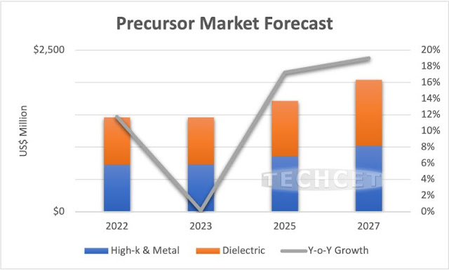
ALD/CVD Precursors – Better Times Ahead
Friday, May 12, 2023
Assessing the Environmental Impact of Atomic Layer Deposition (ALD) Processes and Pathways to Lower It
Assessing the Environmental Impact of Atomic Layer Deposition (ALD) Processes and Pathways to Lower It
Publication Date:April 27, 2023
https://doi.org/10.1021/acsmaterialsau.3c00002
- The thorough optimization of the processing parameters and the reactor design and its infrastructure would drastically lower the undesired wastes and emissions. Computational simulations, machine learning, and artificial intelligence can, for example, be applied to optimize ALD processes faster than ever, as the saturation times can be precisely predicted using these innovative tools.
- High throughput processes such as SALD applied at atmospheric pressure could lead to depositions that are orders of magnitude faster and lower the overall energy budget and related emissions.
- The chemical design of greener precursors would have the largest impact as it could reduce the overall environmental impact: from the raw material extracted and the (limited) number of greener chemistry synthetic steps resulting in the precursor molecules to the thermal budget related to the deposition temperature, and to the emissions of less polluting byproducts.
Friday, May 5, 2023
INFICON xParts ALD Coatings using Picosun P1000
Wednesday, May 3, 2023
AVS ALD2023 & ALE2023 Late News Abstracts Due May 5 - May The 4th Be With You!
|
Forge Nano Partners with Aleon Renewable Metals for Battery Recycling and Supply of ALD Materials for EV Batteries
Tuesday, May 2, 2023
TechInsights found Samsung DRAM chips in Samsung Galaxy S23 with Five EUV mask layers
TechInsights found Samsung DRAM chips in Samsung Galaxy S23 with Five EUV mask layers. These are from DRAM wafers produced in the so-called D1a node (or D1α, α as in alpha)
👉https://t.co/oSv4yiHJiB
— TechInsights (@techinsightsinc) May 1, 2023
Get your products to market faster: @TechInsightsinc found next-gen #DRAM found in the #GalaxyS23. @Samsung is the first company to apply five #EUV lithography masks on DRAM D1a, the first node to fully adopt EUVL for #DRAM. Learn more. #semiconductor pic.twitter.com/2Pqg7gKuE9
This is in line with a previous press release from Samsung (2020) so no real surprise here: Samsung Announces Industry’s First EUV DRAM with Shipment of First Million Modules – Samsung Global Newsroom
"EUV to be fully deployed from 4th-gen 10nm-class DRAM (D1a) next year"
EUV will be fully deployed in Samsung’s future generations of DRAM, starting with its fourth-generation 10nm-class (D1a) or the highly-advanced 14nm-class, DRAM. Samsung expects to begin volume production of D1a-based DDR5 and LPDDR5 next year, which would double manufacturing productivity of the 12-inch D1x wafers.


%20(1).png)


