Friday, November 25, 2022

Applied Materials Delivers Strong FY 2022 Numbers including Picosun ALD

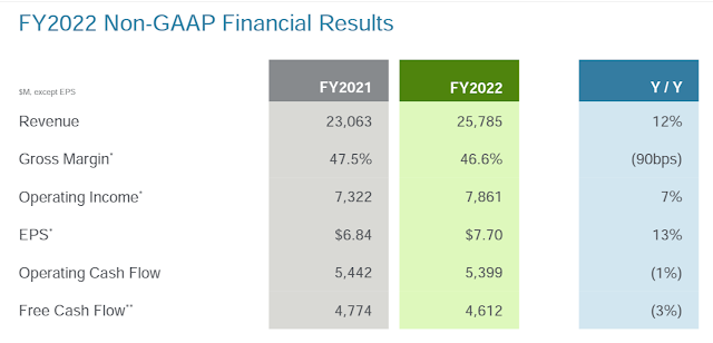
Semiconductor equipment maker Applied Materials has reported strong earnings for FY 2022 (ended October 30). Total sales revenue increased 12% YoY to $25.78 billion despite supply chain shortages, geopolitical and macroeconomic headwinds, and softening consumer demand.

LINK: https://ir.appliedmaterials.com/

The company’s uniquely enabling technology and growing installed base will be its key growth drivers as chipmakers accelerate ramping up of new process nodes in R&D for high-volume manufacturing.


Key developments in FY 2022
  • Applied Materials acquired Picosun, a Finland-based innovator in atomic layer deposition (ALD) technology. This acquisition broadens Applied’s product portfolio and puts it in a great position to capture a large portion of the specialty semiconductor market in the coming years.
  • Collaboration with the Institute of Microelectronics (IME), a research institute under Singapore’s Agency for Science, Technology and Research (A*STAR). IME’s strategic R&D capabilities complement well Applied’s expertise in advanced packaging solutions and will accelerate material, equipment and process technology solutions for hybrid bonding and other emerging, 3D chip integration technologies.
  • Introduced new Ioniq™ PVD system to solve wiring resistance challenges of 2D scaling. This new integrated solution offers a significant reduction in electrical resistance, which has become a critical bottleneck to further improvements in chip performance and power.
Financial highlights
  • Semiconductor Systems revenue increased 15% YoY in FY 2022 to $18,797 million on account of strong orders as customers continued to invest in next-generation technology.
  • Applied Materials’ service revenue increased 11% YoY in FY 2022 to $5,543 million, accounting for 21% of the annual net revenue.
  • Display and Adjacent Markets revenue decreased 19% YoY in FY 2022 to $ 1,331 million.
  • Non-GAAP gross margin was at 46.6% in FY 2022.
  • Non-GAAP operating profit grew by over 7% to $7.86 billion.
  • Non-GAAP EPS increased nearly 13% to $7.70.
  • Total ending backlog increased 62% to $19 billion with Semiconductor Systems backlog increasing 90% to nearly $12.7 billion and services backlog increasing 30% to over $5.6 billion.
  • The company generated about $5.4 billion in operating cash flow and over $4.6 billion in free cash flow.
  • The company’s installed base grew 8% YoY in FY 2022.
  • The number of tools under comprehensive, long-term service contracts grew 16% YoY with the over 90% renewal rate for these agreements demonstrating the value customers see in subscription services.
  • New export regulations for US semiconductor technology sold in China reduced Semiconductor Systems and AGS fourth quarter revenue by approximately $280 million.

Tuesday, November 8, 2022

Recent ALD news on shared on Twitter #ALDep

SparkNano Raises EUR 5.5M to Scale Spatial Atomic Layer Deposition for Energy Applications in a round led by ALIAD Venture Capital by Air Liquide

SparkNano Raises EUR 5.5M to Scale Spatial Atomic Layer Deposition for Energy Applications in a round led by ALIAD Venture Capital by Air Liquide.

SparkNano - LINK (linkmagazine.nl)


Friday, November 4, 2022

ALD coatings for next-generation solar cells

(Helsinki : LINK) Researchers at the University of Helsinki are developing thin films needed in new types of halide perovskite solar cells, and matching ALD processes, in order to provide increasingly affordable solar cells, enable their integration into objects and, consequently, promote the transition to renewable energy.

The 2022 Millennium Technology Prize has been awarded today October 25 to Scientia Professor Martin Green of the UNSW Sydney, Australia, for his innovation that has transformed the production of solar energy.


Members of the research group next to the ALD reactor. Georgi Popov (left), Marianna Kemell, Alexander Weiss and Mariia Terletskaia. (Image: Riitta-Leena Inki)

Most commercial solar cells are silicon-based, and apply PERC (Passivated Emitter and Rear Cell) technology originally launched in 1983 by Martin Green, a recently awarded Millennium Award. However, increasingly efficient, inexpensive and durable solar cells are being developed all over the world. Even in the case of silicon-based cells, a transition is underway to novel techniques, including the tunnel oxide passivated contacts (TOPCon) concept, where several layers of silicon and oxide are added to the cell.

Transparent and flexible solar cells
In addition to silicon, other solar cell technologies are being investigated. The most promising new technique is based on the use of halide perovskites as a light-absorbing material. The general chemical formula of halide perovskites is ABX₃, where A is an alkali metal or an amine, B is tin or lead, and X is a halide. The most commonly studied compound is methylammonium lead iodide CH₃NH₃PbI₃. Perovskite solar cells are on the verge of commercialisation, and some manufacturers believe they will be mainstream in a couple of decades.

“As these new types of solar cells can be transparent, they can be installed in, for example, windows. They are also flexible, which increases their uses,” says Senior University Lecturer Marianna Kemell, who heads the research project funded by the Academy of Finland.

Even though halide perovskite solar cells have achieved high efficiency levels, problems with cell stability and the lack of industrial-scale production techniques have constituted bottlenecks impeding their widespread adoption.

A breakthrough with metal iodides
While pursuing a master’s degree in chemistry, Doctoral Researcher Georgi Popov boldly chose halide perovskites and their atomic layer deposition (ALD) as the topic of his master’s thesis. There were doubters, as prior research-based knowledge was scarce.

“We identified suitable chemicals and were able to design a reaction that enabled us to create a metal iodide coating through deposition for the first time. We were able to demonstrate that this can actually be done through atomic layer deposition. The first successful trial was carried out with lead iodide, which was then processed into CCH₃NH₃PbI₃ perovskite through a further reaction,” Popov says. “The research article was published in the refereed Chemistry of Materials scholarly journal. Later on, we also developed ALD processes for caesium iodide and CsPbI₃ perovskite.”

Coatings produced through atomic layer deposition are used in roughly 30% of silicon-based solar panels. The ALD group headed by Professor Mikko Ritala at the University of Helsinki has achieved promising results in terms of the technique’s adaptability to perovskite solar cells. The advantage of coatings produced by atomic layer deposition is that they form a uniform and comprehensive layer even on rough surfaces.

“If at some point we start making tandem solar cells, which combine a silicon cell and a perovskite cell, we know how to make that perovskite. We are developing the recipes and the chemistry used to grow perovskite,” Popov says.

While the work currently being carried out is basic research, developing recipes and experimenting with small surface areas, the technique is applicable to large-scale production.

“The current plants manufacturing solar cells in China and elsewhere are able to adjust their equipment to produce ALD-coated solar cells,” says Popov.

The future of solar cells
More than 80% of solar cells are manufactured in China, where industrial-scale ALD devices are also produced. Wei-Min Li, PhD, an alum of the University of Helsinki’s Department of Chemistry, works as the chief technology officer at Leadmicro, a leading Chinese manufacturer of ALD equipment. This connection gives the department a solid grasp on where the field is going. ALD equipment used to produce silicon-based solar panels can also be expanded to produce next-generation solar cell materials.

“We are developing the future technical solutions that will gradually replace and supplement current production. In the future, fewer resources will be needed for production, and, thanks to increasingly effective cells, less surface area as well. When solar cells can be installed on uneven surfaces in addition to even ones, we no longer need to build solar parks in fields, as fields are needed for other purposes,” Popov notes.

However, Popov points out that we cannot afford to wait for new technical solutions, as the utilisation of renewable energy sources must be increased now. By replacing current sources of energy with solar or wind power as much as possible, pressure will increase and the entire field will advance.

“The best part of silicon-based cells is that they last roughly 20 to 30 years and will continue to function even after that, albeit possibly less efficiently. Since solar cells produced with the PERC technique are the current state of the art, and they are available, it is advisable to acquire as many of them as possible. They will pay for themselves,” Senior University Lecturer Kemell says.

The project entitled ‘Atomic Layer Deposition as key enabler of scalable and stable perovskite solar cells’, which is funded by the Academy of Finland, will continue until 2024. In addition to Marianna Kemell and Georgi Popov, contributing to the project are Doctoral Researcher Alexander Weiss and master’s student Mariia Terletskaia.

Samsung use NCD ALD for wirebonding alternatives to expensive Gold

According to a recent article by TheElec, Samsung has developed a new chip packaging technology with its key partners for automotive chips. The company employs an aluminum oxide (Al2O3) coating bonding wire technology with improved reliability and insulation compared to previous bonding wires.

Bonding wires connect the I/Os with the lead frame or printed circuit boards. Most of them in the past have been made with gold (Au) as they are flexible and conductive. But as gold prices continue to rise, many companies attempt to mix them with silver (Ag) or copper (Cu). However,  these mixed materials usually have weak adhesiveness with their coating materials. This is unacceptable for chips aimed at automobiles as they are exposed to high-temperature and high-humidity environments.

Samsung’s aluminum alternative, which it is developing with Electron, NCD and LT Metal, doesn’t have this weakness since the aluminum oxide is coated at nanometer thinness onto the metal used as wire. Aluminum oxide bonds well with insulating coating materials that use epoxy. The precursors used to coat the aluminum oxide such as tri-metal aluminum (TMA) are also relatively cheap and used in HVM since a long time.


Insulated, Passivated & Adhesively-Promoted Bond WireUsing All-in-One Al2O3 Coating

Soojae Park(1), Jonghyun Lee(1), Chulhyung Cho(1), Namhoon Kim(1), Yongje Lee(1), Sichun Seo(1), Manho Kim(1), Youngkwon Yoon(1), EulgiMin(2), Kyujung Choi(2), Sang-Hoon Lee(3) Hong-Sik Nam(3),Monghyun Cho(4) & Jeongtak Moon(4),(1)Samsung Electronics Company130 Samsung-Ro, Yungtong-Gu, Suwon-Si, Gyunggi-Do, Republic of Korea(2)NCD Co., Ltd.(3)LT Metal, Ltd.(4)MK Electron Co., Ltd. (2) (PDF) Insulated, Passivated & Adhesively-Promoted Bond Wire Using All-in-One Al2O3 Coating. Available from:

University of Erlangen demonstrate sALD of Crystalline Metal–Organic Framework Thin Films (MOFs)

For the first time, a procedure has been established for the growth of surface-anchored metal–organic framework (SURMOF) copper(II) benzene-1,4-dicarboxylate (Cu-BDC) thin films of thickness control with single molecule accuracy. For this, we exploit the novel method solution atomic layer deposition (sALD). The sALD growth rate has been determined at 4.5 Å per cycle. The compact and dense SURMOF films grown at room temperature by sALD possess a vastly superior film thickness uniformity than those deposited by conventional solution-based techniques, such as dipping and spraying while featuring clear crystallinity from 100 nm thickness. The highly controlled layer-by-layer growth mechanism of sALD proves crucial to prevent unwanted side reactions such as Ostwald ripening or detrimental island growth, ensuring continuous Cu-BDC film coverage. This successful demonstration of sALD-grown compact continuous Cu-BDC SURMOF films is a paradigm change and provides a key advancement enabling a multitude of applications that require continuous and ultrathin coatings while maintaining tight film thickness specifications, which were previously unattainable with conventional solution-based growth methods.

Solution Atomic Layer Deposition of Smooth, Continuous, Crystalline Metal–Organic Framework Thin Films

Maïssa K. S. Barr*, Soheila Nadiri, Dong-Hui Chen, Peter G. Weidler, Sebastian Bochmann, Helmut Baumgart, Julien Bachmann, and Engelbert Redel*
Chem. Mater. 2022, XXXX, XXX, XXX-XXX
Publication Date:November 2, 2022
https://doi.org/10.1021/acs.chemmater.2c01102