ASM used its 2025 Investor Day to set a bold 2030 ambition of more than €5.7 billion revenue, operating margins above 30%, and free cash flow above €1 billion. The company has consolidated a leading position in ALD with over 55% market share in their segments they where they chose to compete and is scaling its Epi business from 12% in 2020 to 25% in 2024. ALD remains the central growth driver, with the market for single-wafer ALD expected to outpace overall wafer fab equipment and reach $5.1–6.1 billion by 2030, while Si Epi is forecast at $2.5–3.2 billion with a 9–13% CAGR.

The single-wafer ALD market is projected to grow strongly from about 3.0 billion dollars in 2024 to between 5.1 and 6.1 billion dollars by 2030, representing a 9–13 percent compound annual growth rate, outpacing the overall wafer fab equipment market, which is expected to grow at 6 percent annually from 110 billion dollars in 2024 to 155 billion dollars in 2030. This growth is driven by the increasing number of ALD layers required in leading-edge logic and foundry processes as well as in advanced DRAM, both in the cell and peripheral CMOS areas. By 2030, ASM aims to maintain a market share above 55 percent, sustaining its lead in logic and foundry while also expanding its position in memory.
Node and memory inflections significantly expand ASM’s served markets, adding $400 million in their served available market from 3nm FinFET to 2nm GAA, and a further $450–500 million from 2nm to 1.4nm, while DRAM transitions contribute another $400–450 million. FEOL ALD layers grow fastest, with roughly 60% of ALD demand at 1.4nm coming from the transistor front end. In advanced packaging, a total available market of $11.5 billion by 2030 supports ASM’s plan to double its served available market to more than 30% of that market.
Services are projected to grow at more than 12% CAGR through 2030, with half of revenues moving to outcome-based models and new “dry clean” refurbish technology delivering ~10× selectivity, ~5× part life, over 95% CO₂e reduction, and more than 2× cost-of-ownership benefits.
ASM also introduced its XP8E common platform integrating clean, treat, inhibit, and ALD steps for 2nm ASD flows, and highlighted AI/ML deployment in high-volume manufacturing for anomaly detection, predictive maintenance, and improved first-time-right performance.

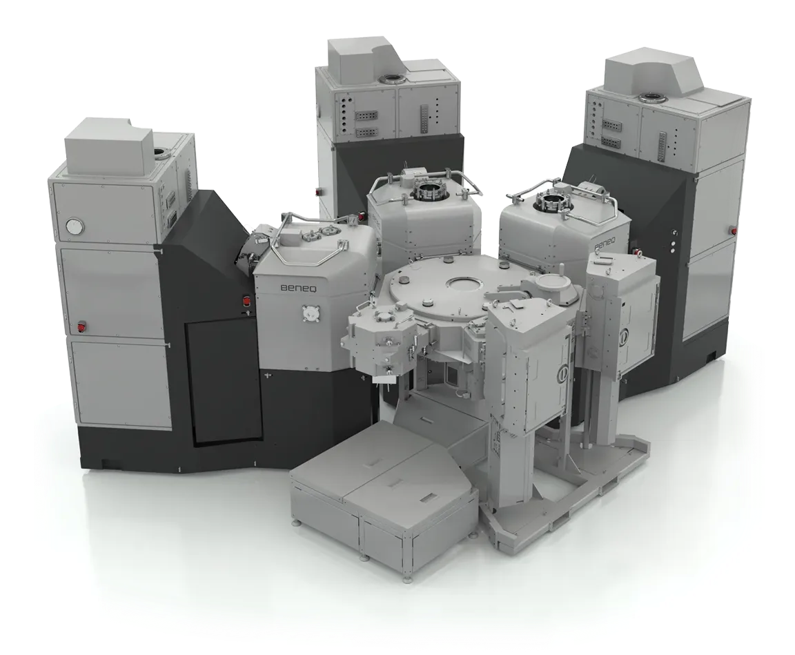
ASM’s XP8E common platform is positioned as a key enabler for the 2nm and beyond era, where Area-Selective Deposition and advanced integration schemes require multiple tightly coupled process steps. By bringing clean, treat, inhibit, and ALD into a single cluster, XP8E reduces wafer handling, shortens cycle times, and improves process control. This integration is critical for scaling as the number of ALD steps grows with each node, and it directly addresses challenges in pattern fidelity, defectivity, and variability that can otherwise undermine yield at 2nm. The platform is designed to be modular and flexible, so customers can configure it for different ASD and high-k/metal gate flows, while also benefiting from a common hardware base that simplifies fab operations, service, and parts management.

Alongside new hardware, ASM is embedding AI and machine learning capabilities into high-volume manufacturing. These tools enable real-time anomaly detection to flag subtle deviations in process behavior before they impact yield, and provide “top contributor” insights that help engineers rapidly identify root causes. Predictive maintenance, including ASM’s PM-Bot automation, improves precision and ensures higher first-time-right rates, cutting downtime and labor intensity. Over time, this creates a closed-loop system where data from thousands of wafers continuously refines process windows, stabilizes tool performance, and enhances cost-of-ownership. In combination, XP8E’s process integration and AI-driven control systems aim to deliver the repeatability, selectivity, and productivity gains required for the 2nm transition and future GAA nodes.
ASMs ALD History - from 1974 to 2024, 50+ years of ALD
The timeline highlights key milestones in the history of ALD and ASM’s leadership in the field. It begins in 1974 with Dr. Tuomo Suntola’s invention of ALD, followed by the founding of Microchemistry in Helsinki in 1987. ASM entered the scene in 1998 with the release of its first 200 mm Pulsar tool and strengthened its position by acquiring Microchemistry from Neste in 1999 and securing Sherman PEALD patents in 2000. Growth continued with the acquisition of Genitech in 2004. In 2008, ASM’s Pulsar tool was recognized as Product of the Year, cementing its reputation. More recently, ASM expanded its product portfolio with the introduction of the dual-chamber Synergis ALD system in 2018, the XP8 quad chamber module in 2019, and the Prominis ALD and XP8E platform in 2024. Strategic acquisitions, such as Reno Sub-Systems in 2022, further enhanced ASM’s technology base, illustrating a steady path of innovation and consolidation in ALD leadership over five decades.

The timeline illustrates ASM’s journey in atomic layer deposition from its origins to modern platforms. ALD was invented by Dr. Tuomo Suntola in 1974, followed by the founding of Microchemistry in 1987. ASM entered the field with the release of its first 200 mm Pulsar tool in 1998, strengthened its position by acquiring Microchemistry from Neste in 1999 (Finland), and expanded its patent base with Sherman PEALD patents in 2000. Key milestones include the acquisition of Genitech (Korea) in 2004, industry recognition for Pulsar in 2008, the introduction of Synergis in 2018 and XP8 in 2019, and the acquisition of Reno Sub-Systems in 2022. Most recently, ASM launched the Prominis ALD and XP8E platform in 2024, underscoring more than 50 years of continuous innovation and leadership in ALD.
The Finnish angle in ASM’s ALD story is both historic and ongoing. Atomic Layer Deposition was invented in Finland in 1974 by Dr. Tuomo Suntola, originally called Atomic Layer Epitaxy. The technology was developed at Microchemistry Ltd., a Finnish company founded in Helsinki in 1987 under Neste. When ASM acquired Microchemistry in 1999, they started gaining the pioneering ALD patents, know-how, and expertise that underpin its leadership today. Finland continues to play an active role through the University of Helsinki and ASM’s Chemical Innovation Group in Helsinki, where precursor chemistry and process research are carried out in close collaboration with Finnish scientists. In this way, Finland provided both the origin of ALD for ASM and remains an important innovation hub supporting ASM’s growth and leadership.
The ASM Pulsar “HIG source” for solids (or the solid precursor delivery subsystem) is a core enabler for ASM’s ability to use low-vapor-pressure solid precursors in ALD. The original innovation from ASM Microchemistry has been further developed over decades and is now still a key technology on the new platform for Molybdenum ALD seen below. It involves a heated sublimation mechanism (sometimes mounted close to or integrated with the reactor), controlled inert gas valves, purge isolation, and precise flux control to feed vapor from a solid into the ALD chamber. The architecture seeks to avoid cold spots or condensation and maintain consistent, controllable precursor delivery pulses.

Genitech was a South Korean company specializing in plasma enhanced ALD and thin film deposition. ASM acquired the company in 2004 to expand its capabilities in plasma based processes and complement its existing thermal ALD portfolio. The acquisition gave ASM a stronger position in PEALD for applications such as high k dielectrics and metal gate stacks used in advanced logic and memory. Genitech’s technology was integrated into ASM’s Pulsar and subsequent platforms, helping establish ASM’s leadership in both thermal and plasma ALD.
ASM acquired Reno Sub-Systems in 2022. Reno is a US-based company specializing in RF power delivery systems and matching networks for plasma tools. Their solid-state RF technology is valued for faster response times, higher precision, and better process stability compared to legacy RF solutions. By integrating Reno’s subsystems into its platforms, ASM strengthened its capability in plasma-based ALD and PEALD, where fine RF control is critical for uniformity, repeatability, and advanced film properties.
Future Outlook
ASM ties its deposition processing capability to its tool portfolio—Pulsar, EmerALD, Synergis, Prominis, XP8E, and others—which are engineered with small-volume reactors, advanced plasma control, and integrated multi-step clustering (clean, treat, inhibit, deposit).
Looking ahead, ASM is uniquely positioned to remain the clear leader in atomic layer deposition as the semiconductor industry advances to 2nm and beyond. The company’s deep history in ALD, dating back to Dr. Tuomo Suntola’s invention in 1974, has evolved into a robust technology portfolio that now commands more than 55 percent market share where ASM chooses to compete.
With single-wafer ALD forecast to nearly double in size by 2030 and outpace overall wafer fab equipment growth, ASM is set to capture outsized value from both logic and memory inflections. Its proven expertise in solid source precursor delivery, trailing back to the the Pulsar HIG sublimation system and F120 Microchemistry research reactors, now expands to new material capabilities such as molybdenum ALD for advanced node metallization. At the same time, ASM is broadening its impact through the XP8E common platform, which integrates multiple critical steps into one cluster with embedded AI and machine learning into high-volume manufacturing for real-time control. ASM’s combination of process innovation, equipment integration, and data-driven intelligence places the company at the center of semiconductor scaling, ensuring its leadership in enabling Moore’s Law through the next decade.
Sources:


%20(1).png)