


%20(1).png)
Espoo, Finland, 14 July 2025 – Beneq, a global leader in Atomic Layer Deposition (ALD) technology, has announced significant momentum in the microLED display sector, marked by repeat orders from leading tech innovators. The development highlights the growing demand for advanced manufacturing tools capable of supporting the next generation of display technologies.
MicroLED is increasingly seen as a transformative display technology across consumer electronics, augmented and virtual reality (AR/VR), and the automotive sector. Offering superior brightness, contrast, energy efficiency and durability, microLED enables ultra-fine resolution, longer device lifetimes and seamless scalability.
According to Yole Group, global microLED display shipments are expected to grow at a compound annual rate of 180.6 percent from 2022, reaching 42.4 million units by 2029. However, manufacturing challenges remain, particularly as pixel sizes shrink below 10 micrometres. ALD plays a critical role in overcoming these hurdles by delivering ultra-thin, conformal coatings that ensure uniformity, stability and surface passivation—key for improving efficiency and reliability.
“Our top-tier customers rely on ALD technology to advance monolithic integration of microLEDs and driver electronics on a single chip,” said Mikko Söderlund, Head of Semiconductor ALD Sales at Beneq. “This enables a new class of compact, high-performance display products with faster data transfer and reduced power consumption.”
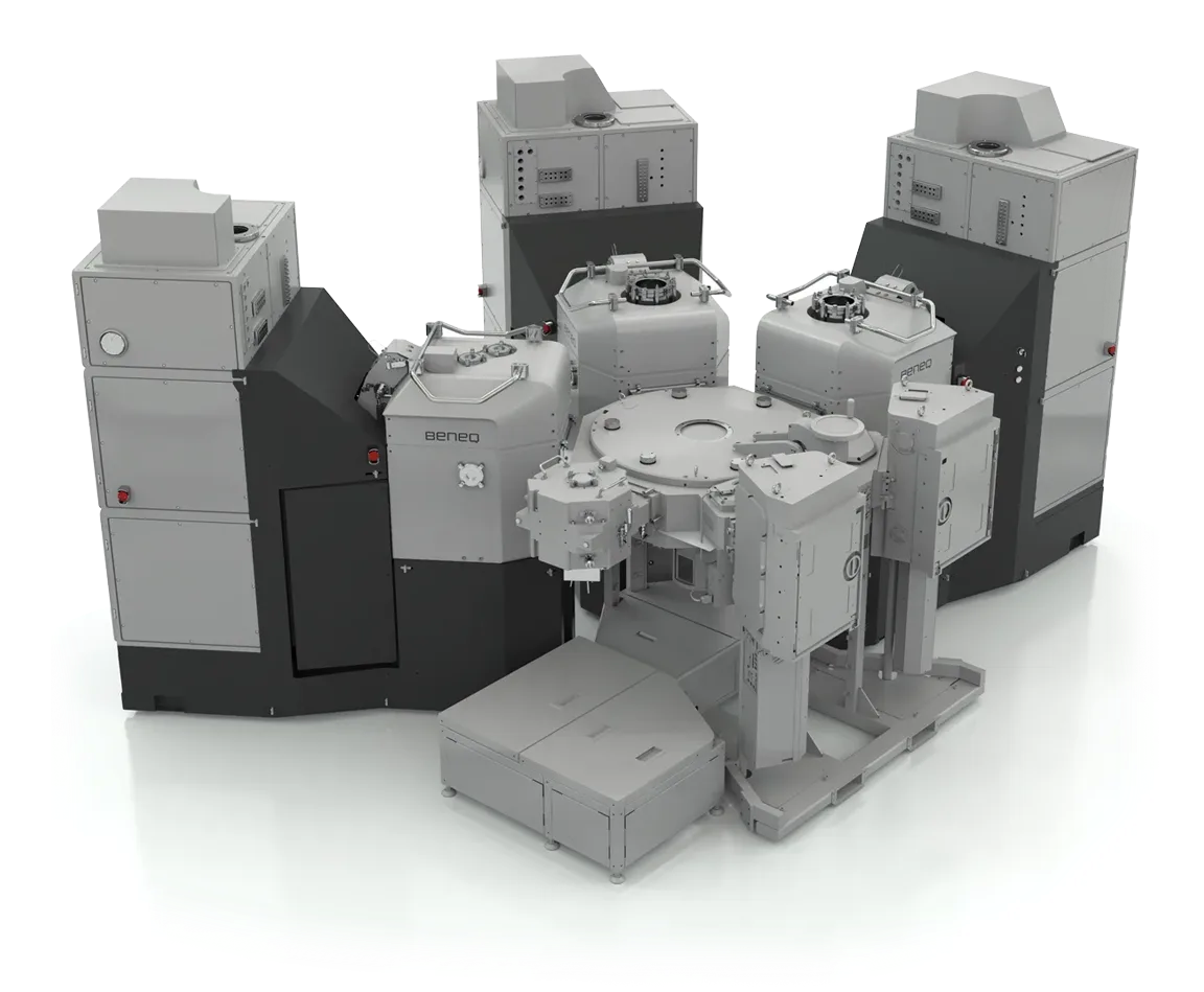
Beneq’s Transform® ALD cluster platform is central to its offering, providing high-throughput production capability with a modular, multi-chamber design. The platform supports a range of materials and processes, allowing customers to optimise optical and electrical properties while scaling from lab to fab.
These developments reinforce Beneq’s commitment to supporting microLED pioneers through both early-stage development and the transition to volume manufacturing, accelerating the path toward widespread adoption of advanced display technologies.
Sources:
Beneq Advances MicroLED Leadership with Growing Demand from Industry Frontrunners | Beneq

.jpg)


.jpg)
.png)


