Thursday, November 30, 2017

2nd HERALD.ECI Workshop in Barcelona March 1-2, 2018

The main objective of this 2nd HERALD.ECI Workshop with hands-on training is to
create an ignition point for competitive proposals resulting in joint, EU-funded research projects
under ECI
(early career investigator) participation or leadership.
We want the trainees to
  • gain advanced ‘theoretical’ knowledge input on how to write competitive proposals & manage EU-funded projects from an EU funding expert & Horizon 2020 coach through an impulse talk plus interactive proposal clinics.
  • find excellent, perfectly matching collaboration/ project partners during a welcome mixer.
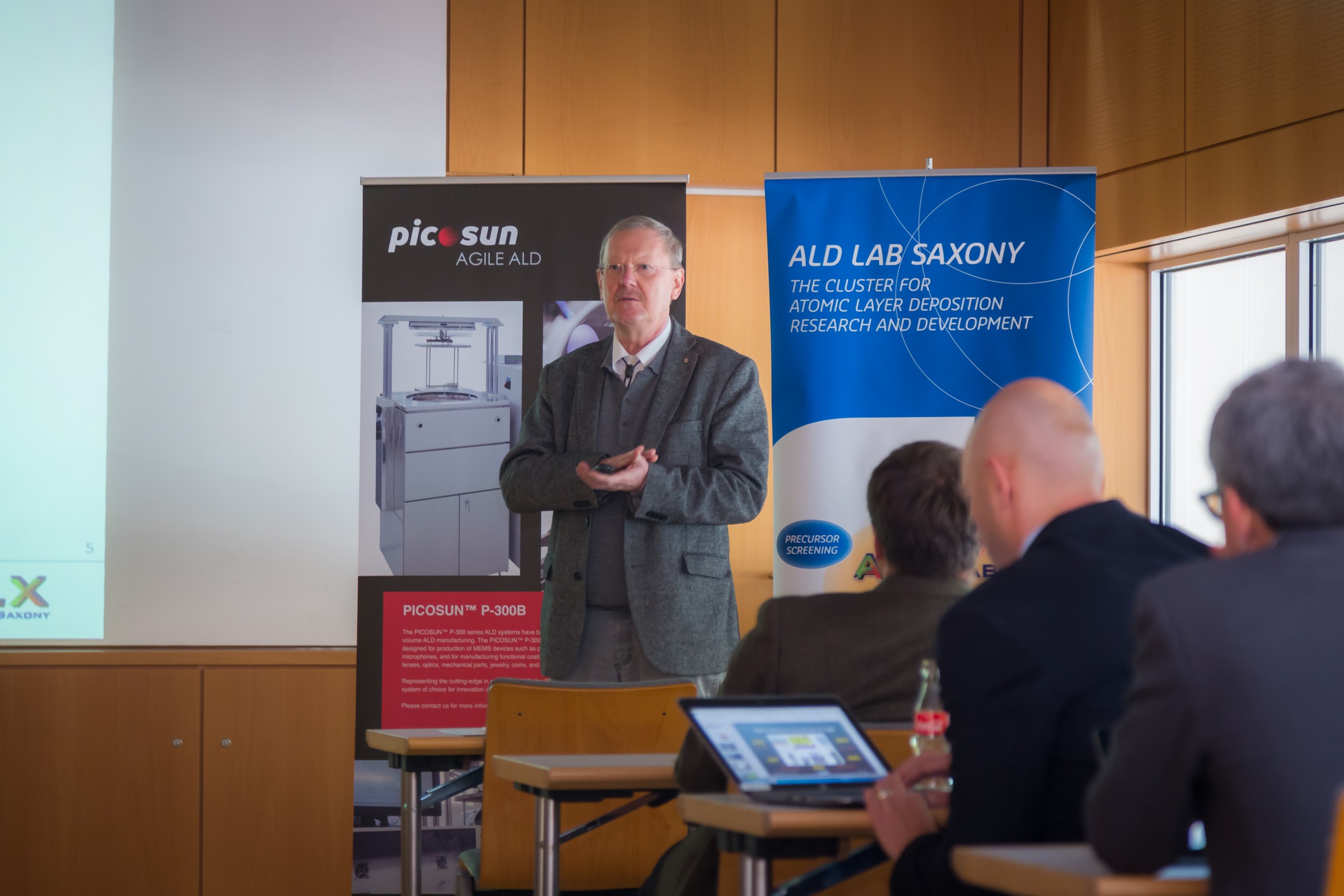
  • exchange experiences with an excellent (female) ALD expert and with an industry partner.
  • transfer the newly gained knowledge into advanced ‘practical’ skills by
    developing joint proposal ideas,
    transitioning specific ideas into concrete proposal drafts, and
    starting to write
    together in smaller, matched collaboration/ project groups.
  • go home with a raw outline and concrete idea description, i. e. the first step of an actual proposal.

Agenda

The complete Agenda in all detail will be updated here soon.

tentative Agenda as of November 28, 2017


Wednesday, November 29, 2017

Transparent flexible capacitors by ALD high-k, ALD AZO and graphene electrodes

Transparent and flexible flat panel displays manufactured on plastic substrates and flexible substrates involve key technologies like ALD manufacturing of transparent electrodes and barriers. In addition, for the pixel-drive circuit of displays, capacitors are used for charging and discharging at very high speed. Having a high capacitance enables also a high color brightness for each pixel. Now researchers at Wuhan University, China has developed an capacitor technology that is has an excellent transparency and flexibility using the latest ALD and graphene processing technology. Please find the Open Access publication below.

In this study used comercially available graphene in the form of single-layer graphene that had been grown by CVD on copper foil from 2D Carbon Tech Inc. LTD, Changzhou, China. The ALD ZrO2 high-k and AZO was grown in an TSF 200 from Beneq.

Transparent and Flexible Capacitors with an Ultrathin Structure by Using Graphene as Bottom Electrodes
by Tao Guo, Guozhen Zhang, Xi Su, Heng Zhang, Jiaxian Wan, Xue Chen, Hao Wu and Chang Liu
Nanomaterials 2017, 7(12), 418; doi:10.3390/nano7120418  (registering DOI) - 28 November 2017
 
 
(Left) The schematic diagram of the ultrathin, transparent and flexible capacitors; (Right) The optical transmittance spectra of the capacitors on PEN substrates. The inset shows the optical photograph of the actual capacitor device with the characters “TFS 200” in the background, and the optical transmittance spectra of graphene and capacitors on quartz substrates. 
 
Ultrathin, transparent and flexible capacitors using graphene as the bottom electrodes were directly fabricated on polyethylene naphthalate (PEN) substrates. ZrO2 dielectric films were deposited on the treated surface of graphene by atomic layer deposition (ALD). The deposition process did not introduce any detectible defects in the graphene, as indicated by Raman measurements, guaranteeing the electrical performances of the graphene electrodes. The Aluminum-doped zinc oxide (AZO) films were prepared as the top electrodes using the ALD technique. The capacitors presented a high capacitance density (10.3 fF/μm2 at 10 kHz) and a relatively low leakage current (5.3 × 10⁻⁶ A/cm2 at 1 V). Bending tests revealed that the capacitors were able to work normally at an outward bending radius of 10 mm without any deterioration of electrical properties. The capacitors exhibited an average optical transmittance of close to 70% at visible wavelengths. Thus, it opens the door to practical applications in transparent integrated circuits. Full article

This is an open access article distributed under the Creative Commons Attribution License which permits unrestricted use, distribution, and reproduction in any medium, provided the original work is properly cited. (CC BY 4.0).

Picosun provide ALD Cluster Tool to Swedish MEMS Foundry Silex Microsystems

ESPOO, Finland, 29th November, 2017 – Picosun Oy (Finland), Silex Microsystems AB (Sweden), and Pegasus Chemicals Ltd (UK) have joined forces to develop and provide novel ALD (Atomic Layer Deposition) solutions and processes for MEMS (MicroElectroMechanical Systems) industries. The aim of the collaboration is to realize emerging, advanced MEMS structures that would not be possible to manufacture by any other thin film deposition methods.


Today, MEMS are crucial components in several everyday applications such as mobile phones, cars and in various sensor systems. In addition to these already vast markets, the rapidly spreading Internet-of-Things with its billions of independently communicating electronic devices is a huge driving force to accelerate MEMS industry’s exponential growth in the very near future. 
 

This is Silex Microsystems (Promotion Viedo from Youtube)
 
In the Picosun-Silex-Pegasus collaboration, a PICOSUN™ ALD cluster platform is installed at Silex’s MEMS foundry in Järfälla, Sweden. The platform consists of a fully automated, factory integrated cassette-to-cassette vacuum robot for substrate handling and a PICOSUN™ P-300F ALD reactor capable of coating up to 25 pcs 8” wafers in a batch. The installed reactor can deposit various metal oxides, metal nitrides, and pure metals on up to tens of thousands of wafers per month (*). Pegasus develops and manufactures the precursor chemicals required for the ALD processes and provides the technical support and delivery options for individual applications. The cluster platform can be later upgraded with two additional ALD reactors. In the collaboration, engineers and scientists from all three partners work together to solve existing problems in MEMS processing, as well as to develop completely new openings on how to realize novel MEMS devices.

“We have been working with Picosun since 2010 and now with this project we can bring our collaboration to a completely new level. We are very excited to have the PICOSUN™ ALD cluster platform in our cleanroom. It enables us to develop novel, production-proven ALD solutions for our customers in advanced MEMS applications,” says Dr. Niklas Svedin, Vice President of Engineering at Silex Microsystems. 
“This is a valuable project for us, as the use of ALD in MEMS processing is increasing very fast. We have already strong presence in the MEMS market, but new applications come up weekly and we want to keep our spearheading position in this development. Now in the SALADIN project we have partners with whom we can also test and develop new ideas of our own how ALD could be implemented in the MEMS process flow,” continues Mr. Juhana Kostamo, Managing Director of Picosun. 
 
“The MEMS industry is a fast-growing market and it is very interesting for us to be involved in the process of introducing the groundbreaking ALD cluster platform to it. We are eager to be in the frontline of the chemical development for this field and focusing on advanced MEMS applications,” summarises Dr. Paul Williams, Technical Director of Pegasus Chemicals. 
 
Picosun Oy (LINK)
Silex Microsystems (LINK)  
Pegasus Chemicals (LINK)

(*) Throughput calculated for 10 nm Al2O3, 90% system uptime.

Saturday, November 25, 2017

The 7nm race by TSMC and Samsung - EUV or not EUV

According to industry sources on October 19, Samsung Electronics is considering a plan to purchase 10 extreme ultraviolet (EUV) lithography tools from the Netherlands-based ASML, the biggest semiconductor equipment maker in the world. To put tha in perspective - ASML believes that it can produce about 12 EUV lithography tools this year. It is the only company that manufactures EUV lithography tools in the world.

Sales in ALD and Etch equipment have been boosted by multiple patterning technologies based on Immersion lithography, both for Logic/Foundry and Memory. Maybe as much as 1/3 of the single/multi wafer ALD equipment market is patterning related. The last two years or so analyst have been busy trying to figure out the impact on deposition and etch equipment sales if/when EUV is introduced. Here is a recent take down by Seeking Alpha (LINK). My view is that scaling is based on symbiotic use of the latest technologies and multiple patterning and EUV will co-exist and keeping the scaling path alive. In addition, scaling opens new opportunities for ALD, ALEtch and future use of selective growth technologies with atomic scale precision. According to recent reports the ALEtch market segment is now considerd an actual segment by itself and has entered HVM (LINK).
Fudzilla reports: Korean based ETNews has mentioned that Qualcomm 7nm manufacturing has been a big win for TSMC while two other US and China customers chose Samsung’s 7nm. TSMC traditionially have dibs on Nvidia and MediaTek according to the report.

Qualcomm and Broadcom, according to the report are designing their next generation chips with TSMC’s7-nano PDK. The reason why Qualcomm went with 7nm with TSMC is the fact that the fab uses normal steppers while Samsung wants to make its 7nm with more bold and riskier EUV (Extreme Ultraviolet) photolithography technology.

View of Samsung Electronics’ Hwasung 17 line. It is expected that Samsung Electronics will build a new 7-nano plant on a nearby site according to ETNews.

Samsung is expected to be later to the 7nm game and early adopters had to go with TSMC. EUV is still technology that is not entirely ready for the mass market and there is a disagreement weather you should need to use Extreme Ultraviolet light manufacturing with 7nm or first with 5nm. Obviously the two main fabs disagree while GlobalFoundries cooperates and shares technology with Samsung, and will have Samsung to rely upon for 7nm.

Full article: Qualcomm 7nm made by TSMC [LINK]
ETNews original source: Samsung Electronics Close to Securing Two New Customers for Its 7-Nano Foundry[LINK]
Business Korea: Keeping Leadership in 7-nano Era Samsung Electronics Seeks to Buy Up Next-gen Semiconductor Mfg Equipment

Monday, November 20, 2017

ALD assisted Nano-Architected capacitors

Nanotechweb.org reports: Researchers at Gwangju Institute of Science and Technology (GIST) Korea and California Institute of Technology USA have made low-k dielectric by a new technique. They deposit a photoresist on the top of a electrode (Au/Ti (80/12 nm) and then directly write a nanolattice scaffold into the photoresist layer using a technique called two-photon photolithography direct laser writing. 

They then coat coated the polymer nanolattice with a 10 nm-thick conformal layer of alumina (Al2O3) using atomic layer deposition (ALD) and etch away the photoresist by an oxygen plasma using a focused ion beam. Finally, we evaporated an identical Au/Ti (80/12 nm) bilayer as a top electrode on the top plate of the nanolattice to create a parallel plate capacitor.

Please find much more details in this Nanotechweb.org article (LINK) and the publication below:

Enabling Simultaneous Extreme Ultra Low-k in Stiff, Resilient, and Thermally Stable Nano-Architected Materials 

Max L. Lifson, Min-Woo Kim, Julia R. Greer, and Bong-Joong Kim
Nano Lett., Article ASAP
DOI: 10.1021/acs.nanolett.7b03941 
Publication Date (Web): November 7, 2017

Abstract Image

Low dielectric constant (low-k) materials have gained increasing popularity because of their critical role in developing faster, smaller, and higher performance devices. Their practical use has been limited by the strong coupling among mechanical, thermal, and electrical properties of materials and their dielectric constant; a low-k is usually attained by materials that are very porous, which results in high compliance, that is, silica aerogels; high dielectric loss, that is, porous polycrystalline alumina; and poor thermal stability, that is, Sr-based metal–organic frameworks. We report the fabrication of 3D nanoarchitected hollow-beam alumina dielectrics which k is 1.06–1.10 at 1 MHz that is stable over the voltage range of −20 to 20 V and a frequency range of 100 kHz to 10 MHz. This dielectric material can be used in capacitors and is mechanically resilient, with a Young’s modulus of 30 MPa, a yield strength of 1.07 MPa, a nearly full shape recoverability to its original size after >50% compressions, and outstanding thermal stability with a thermal coefficient of dielectric constant (TCK) of 2.43 × 10⁻⁵ K–1 up to 800 °C. These results suggest that nanoarchitected materials may serve as viable candidates for ultra low-k materials that are simultaneously mechanically resilient and thermally and electrically stable for microelectronics and devices.

Annual High-k Workshop 2018 goes on excursion to Wroclaw Poland

This coming year the classic Dresden NaMLab annual High-k Workshop 2018 organized by Dr. Uwe Schröder (ALD2012, Co-Chair) will make an excursion to Wroclaw Poland. The webpage just came online so please check it out for further details on the event.

Conference "High-k oxides by ALD"

Hotel Jasek Premium, Wrocław, Poland, March 7th - 10th, 2018 

In collaboration with the EU COST networking project HerALD, Institute of Physics, Polish Academy of Sciences and Polish Vacuum Society invite you to the next edition of the conference "High-k oxides by ALD", which will be held in Wroclaw, Poland, on March 7-10, 2018. New challenges offered by the application of ALD based high-k dielectric materials in nanotechnology will be discussed by more than 80 participants from industry, research institutes and universities.

The conference is continuation of NaMLab workshops - a stimulating European platform for application-oriented scientists to exchange ideas and discuss latest experimental results on process technology, new results in the field of ALD-grown dielectrics for solar cells, transparent conduction oxides (TCOs), and for silicon based micro- and nano-electronics. The 2018 edition is organized in Poland to increase integration between Eastern and Western Europe countries. 


Beautiful Ostrów Tumski ("Cathedral Island", German: Dominsel) is the oldest part of the city of Wrocław in south-western Poland. It was formerly an island (ostrów in Old Polish language) between branches of the Oder River [Wikipedia].

Sunday, November 19, 2017

Atomic Layer Etching is entering HVM for sub 14 nm Logic

After years in R&D, several fab tool vendors last year finally began to ship systems based a next-generation technology called atomic layer etch (ALE).

ALE is is moving into 16/14nm, but it will play a big role at 10/7nm and beyond. The industry also is working on the next wave of ALE technology for advanced logic and memory production.

Used by chipmakers for years, traditional etch systems remove materials on a continuous basis in devices. Considered a next-generation etch technology, ALE selectively removes targeted materials at the atomic scale without damaging other parts of the structure. For example, ALE can be used to remove materials in a structure to form trenches with gaps on the order of 10 to 15 angstroms or 5 atoms wide. (An angstrom is 0.1nm.)

Applied Materials Centris Sym3 is one of the Applied Materials offering for ALE. It can be configured to handle plasma ALE for anisotropic etch applications, such as self-align contacts and spacer-based patterning.

Applied Materials, Hitachi High-Technologies, Lam Research and TEL are among the suppliers of ALE tools in the market. Today, ALE represents a tiny percentage of the overall etch market. In total, the worldwide dry etch business is projected to reach $9.6 billion in 2017, up from $7.2 billion in 2016, according to Gartner.

Full article :  "What’s Next For Atomic Layer Etch?" by Mark Lapedus, Semiconductor Engineering (LINK)


Saturday, November 18, 2017

Aixtron complete sale of ALD/CVD memory product line to Eugene Technology

AIXTRON SE (FSE: AIXA), one of the world’s leading providers of deposition equipment to the semiconductor industry, announced today that the sale of AIXTRON’s ALD and CVD memory product line to Eugene Technology Inc., a wholly owned U.S. subsidiary of Eugene Technology Co., Ltd, South Korea was completed as of November 15, 2017. 

The QXP-8300 Atomic Layer Deposition (ALD) mini-batch system suitable for e.g. high-k oxide films in advanced memory applications including 3D structure devices (aixtron.com)

AIXTRON will receive c. USD 60 million for the assets being transferred and c. USD 11 million for open supplier orders for which it retains the liability to pay.

AIXTRON, Inc., the U.S. subsidiary of AIXTRON SE situated in Santa Clara, California, will continue to provide sales and support for its continuing businesses.

Arradiance and InRedox team up to offer ALD Functionalized Nanomaterials

SUDBURY, Mass., Nov. 17, 2017 —Arradiance’s formidable Atomic Layer Deposition (ALD) foundry service and InRedox’s world-class manufacturing of nanoporous anodic aluminum oxide (AAO) and nanotubular anodic titanium oxide (ATO) will provide new ALD-functionalized Nanoceramics for life sciences, nanotechnology, filtration and separation, energy generation and storage, analytical equipment and many other applications.
 

Arradiance LLC, manufacturer of the popular GEMStar family of professional, research grade Atomic Layer Deposition (ALD) systems and provider of nanofilm foundry services, today announced a partnership with InRedox LLC (Longmont, Colorado) to provide nanotechnology researchers with ALD-functionalized nanostructured materials (wafers, membranes and nanotemplates).

“InRedox’s innovative AAO / ATO wafers and templates have demonstrated utility at leading commercial, academic and government research institutions across a broad range of technology areas,” said Arradiance CEO Michael Trotter. “I am certain that the combination of Arradiance’s ALD nanofilms with InRedox’s powerful nanofabrication technology platform will spur exciting new developments,” explained Mr. Trotter.

“InRedox is excited by the potential of ALD functionalized nanoporous ceramics,” stated Dmitri Routkevitch, InRedox President and CTO, “and we look forward to working with Arradiance to continue to expand the range of nanomaterials that inspire and enable our customers in their pursuit of scientific breakthroughs or new products.”

Thermal atomic layer deposition of tungsten carbide films from WCl6 and TMA

Kyle J. Blakeney and Prof Winter from Department of Chemistry, Wayne State University just published a new exciting ALD path to tungsten carbide. WCl6 has favorable precursor characteristics and advantages over the widely used WF6, which is corrosive and toxic. In addition, fluorine tend to diffuse into dielectric layers (SiO2, SiN, high-k) and can cause reliability issues for transistor and memory devices e.g. in CMOS Logic, DRAM and NAND Flash Memory.

Films for this study were deposited in a Picosun R75-BE ALD reactor and WCl6 (99.9%, Strem)  delivered at 125 °C using the solid state booster in the reactor. You may find more details an the ALD redactors at their lab here (LINK).

Please check out the publication in JVSTA A - Open source available for all!

Free, Published Online: November 2017Accepted: October 2017
Journal of Vacuum Science & Technology A: Vacuum, Surfaces, and Films 36, 01A104 (2018); https://doi.org/10.1116/1.5002667

Nice little story on thermal #ALDep of tungsten carbide online now. TMA is definitely the most versatile ALD precursor https://t.co/65yNQpNcDl
Also nice to see the refernce No. 33 to this Blog :-)


Thursday, November 16, 2017

Beneq present ALD Throughput Revolution in More than Moore Markets

At Semicon Europa, the largest microelectronics event in Europe, 14-17, November, Munich, Germany, Beneq launched the Beneq C-Series, a new Cluster-Compatible ALD product family for high-volume manufacturing of wafers. This is the start of a throughput revolution for ALD in new More than Moore wafer processing markets. 


Beneq C2 is a cluster-compatible automated wafer ALD system for industrial processing of wafers. It is available both as a single-wafer version and as batch-processing equipment for high volume manufacturing. Beneq C2 offers a unique combination of high capacity batch processing and standard cassette-to-cassette automation. Each process module on the cluster can process up to 30 000 wafer passes per month(200 mm wafers). [beneq.com]

Please find more detailed information in the press release from Bebeq [LINK]


Wednesday, November 15, 2017

According to Amnesty Industry giants fail to tackle child labour allegations in cobalt battery supply chains

According to Amnesty International, major electronics and electric vehicle companies are still not doing enough to stop human rights abuses entering their cobalt supply chains, almost two years after an Amnesty International investigation exposed how batteries used in their products could be linked to child labour in the Democratic Republic of Congo (DRC), the organization said today.

- Survey of electronics and car companies shows major blind spots in supply chains
- Apple is the industry leader for responsible cobalt sourcing – but the bar is low
- Microsoft, Lenovo and Renault have made least progress


RATING COMPANIES
All possible actions taken None
Adequate action taken Apple - Samsung SDI
Moderate action taken Dell - HP - BMW - Tesla - LG Chem
Minimal action taken Sony -Samsung Electronics - General Motors - Volkswagen - Fiat-Chrysler - Daimler - Hunan Shanshan - Amperex Technology - Tianjin Lishen
No action taken Microsoft - Lenovo - Renault - Vodafone - Huawei - L&F - Tianjin B&M - BYD - Coslight - Shenzhan BAK - ZTE


 Movement of cobalt, from mine to global market [Source: Amnesty International]

In parallel ther are roports on price of Cobalt "Cobalt Prices to Rocket" : The Democratic Republic of Congo supplies some 60 percent of the world's cobalt- a desperately sought after metal that is the driver of our electric vehicle (EV) boom and the fodder of battery gigafactories popping up all over the world.

Buyers are under growing pressure to give up conflict cobalt and find new sources, but the timing is tough. Major automakers and battery manufacturers are scrambling to secure supplies of cobalt. Prices are soaring, and demand can only move in one direction - up.

One company in the heart of the Cobalt supply chain that do care a lot about fair and ethical sourcing of Cobalt is Umicore, please see previous report ebout their supply chain here - Umicore's pioneering approach to ethical cobalt sourcing for CVD/ALD precursors [LINK].

An industry that is not included here in the Amnesty study that has been using wast amounts of Cobalt for a long time is for instance the cemented carbide industry for hard metal tooling.

Sources:

Amnesty International - Industry giants fail to tackle child labour allegations in cobalt battery supply chains
https://www.amnesty.org/en/latest/news/2017/11/industry-giants-fail-to-tackle-child-labour-allegations-in-cobalt-battery-supply-chains/

Cobalt Prices to Rocket as Tech Giants Scramble for Supplies
https://www.prnewswire.com/news-releases/cobalt-prices-to-rocket-as-tech-giants-scramble-for-supplies-657690933.html

ALD Lab Saxony Symposium at Semicon Europa 2017

The ALD Lab Saxony just held its annual Symposium at SEMICON Europe in Munich, Germany. Prof. Bartha, Dr. Jonas Sundqvist, Dr. Martin Knaut and Dr. Christoph Hossbach have been organizing the event since 2012 in Dresden. This year about 50 persons attended the symposium.

The Intention of the Symposium is to improve visibility of the Atomic Layer Deposition technique and its capabilities and to increase the networking within the ALD community. The given talks gave an overview of current research and development topics as well as examples of ALD applications, equipment, chemical and supply chain in manufacturing. This year’s agenda combined several talks from ALD Lab Saxony members and partners from academia and industry on ALD equipment, applications, metrology as well as ALD simulations. This year the symposium was divided into two sessions: “Equipment and Applications” and “Precursors, Precursor Delivery, Metrology and Simulations”

New exciting applications in the field of MEMS were presented by Fraunhofer ISIT, ALD corrosion protection by Bosch and metal precursor sourcing and supply chain solutions by Umicore to mention a few. The complete Agenda can be found here (LINK: http://www.semiconeuropa.org/ald-lab-symposium-2017) and upon request the presentations will become available.

“Welcome”, Prof. Bartha, TU Dresden (Germany)

“ALD for Production”, Dr. Christoph Hossbach, Picosun (Finland/Germany)

“ALD equipment and precursors for high volume manufacturing”, Dr. Jonas Sundqvist, Fraunhofer IKTS (Germany) /TECHCET LLC (USA)


“ALD process monitoring with quartz crystal microbalances”, Dr. Martin Knaut, TU Dresden (Germany)

Friday, November 10, 2017

Picosun Oy shows record growth in ALD for fiscal year 2016/2017

Picosun is one of the leading suppliers of ALD thin film deposition technology for semiconductor, lightning, MEMS as well as for other industries and research. This week I had the chance to meet with Kustaa Poutiainen himself, Chairman and Chief Executive Officer of Picosun Oy. in Dresden. We had a very interesting meeting discussing recent developments in ALD Technology announced by Picosun as well as discussing the past and future outlook of ALD.   

Mr Poutiainen was in Germany to meet with customers and overseeing Picosuns activities and expansion in Germany. In the European perspective Germany is the biggest market for ALD Technology and Equipment. For those of you who do not know, Picosuns ALD equipment portfolio in detail it ranges from fully automated ALD batch and cluster systems for high volume manufacturing to smaller scale R&D and pre-pilot production tools (see below). 


A snapshot of the Picosun products - more information here.
Picosun has recently opened a branch office in Germany - Picosun Europe GmbH, headed by General Manager Dr. Christoph Hossbach, serving its growing install base of ALD equipment on the German market, both at leading research institutes within Fraunhofer and other research organizations and wafer fabs. According to previous press releases made we know that they have a number of high value customers in Germany including Bosch Sensortech.

Mr Poutiainen was very excited over the development of Picosun as a company and informed me that it ended its Fiscal year 2016/2017 in September by a record turnover growth of 27% landing at just above 21 million EUR for 2016/2017 and more details will be released soon. The company is constantly investing to develop it operations further globally adding new local teams and having a strong focus on R&D. Mr Poutiainen did also let me know that Picosuns R&D expenses are at about 20% of the actual turnover, which is considerable. Quoting Mr Poutiainen: “The most awarding proof of success of the company is to hire new members. We are looking to hire more than 30 new employees in the next expansion phase”.
Next you have a chance to meet Picosun at SEMICON Europa in Minich. Picosun is exhibiting as well as sponsoring the ALD Lab Saxony Symposium on the 14th of November.
ALD Lab Saxony Symposium : LINK


Thursday, November 9, 2017

Oxford Instruments and das-nano demonstrate non-destructive wafer based thickness and resistivity metrology for PEALD TiN


Commonly titanium nitride (TiN) thickness and resistivity wafer fab in-line metrology is based on ellipsometry and 4-point probe resistivity mapping. Alternative and relatively slower or more complex methods are X-ray photoelectron spectroscopy (XPS), X-ray reflectivity (XRR) and X-ray fluorescence (XRFS). TiN thin films are highly conductive and lose transparency for thicker layers which can make it challenging to accurately measure the thickness by ellipsometry above 10-20 nm. At about 50 nm layer thickness TiN is non-transparent and has a bronze color changing to gold for even thicker layers. In the case of resistivity mapping, 4-point probe is a destructive method leaving scratches from the needles that penetrates the TiN layer and possibly also damages the underlying layers and devices.

Atomic Layer Deposition of TiN on 200 mm wafers

TiN is used as a metal gate in complementary metal-oxide-semiconductor (CMOS) technology as it has low resistivity and is compatible with gate dielectrics. TiN is also deposited as a wear resistant coating, and barrier layer for copper diffusion due to its chemical and thermal stability. Traditionally TiN was deposited using physical vapour deposition techniques which suffer from as poor step coverage in deep contacts and via trenches due to the shadowing effects especially in high aspect ratio structures. 

Atomic layer deposition (ALD) is a thin film deposition technique which allows for Å-level control of the film thickness, excellent uniformity, and conformal coating of high aspect ratio features. 

Therefore, non-destructive characterization of thickness and electrical uniformity across the entire surface covered by the deposition is critical to ensure the quality of the final film. Oxford Instruments demonstrate the deposition of conductive TiN by plasma enhanced ALD with excellent thickness uniformity and collaborate with das-nano to map the resistivity uniformity using THz spectroscopy on 200 mm wafers. 


Read the full report here [Link to download paper]