The Oxford Instruments Innovation Centre, a state-of-the-art facility, has been launched at its High Wycombe site. This Centre consolidates Oxford Instruments' analytical innovations, aligning with its mission of fostering a greener, healthier, more connected society. The inauguration welcomed dignitaries like Countess Howe, Lord-Lieutenant of Buckinghamshire, and Cllr. Paul Turner, Mayor of High Wycombe, alongside prominent figures from academia and industry. Dr. Ian Wilcock, Managing Director, led the opening, showcasing the Centre's role in advancing scientific research in various fields. The facility, a collaboration hub, allows access to cutting-edge technology and expertise. Oxford Instruments, a pioneer since 1959 and a significant contributor to Nobel-prize winning research, continues to impact science, particularly in material analysis, underlining its global technological leadership.
Oxford Instruments has received significant orders for its GaN ALE (Atomic Layer Etch) and ALD (Atomic Layer Deposition) systems from major Japanese foundries specializing in power electronics and RF (Radio Frequency). These systems are essential for producing GaN (Gallium Nitride) HEMT (High Electron Mobility Transistor) devices, catering to rapidly growing markets such as consumer fast-charging, data centers, and 5G/6G communications.
The company's ALD technology is known for its high throughput and low damage plasma processing, enhancing film and interface quality. It is widely used by leading GaN HEMT device manufacturers globally. The ALE solution, particularly for p-GaN HEMTs, is production-qualified and offers precise etching with minimal damage, featuring Etchpoint®, a unique endpoint detection technology developed in collaboration with LayTec AG.
Atomic Scale Processing
Etchpoint® allows for automated transition from standard high-rate etching to low damage ALE, improving device reliability. It enables precise AlGaN recess etches, crucial for the next generation GaN MISHEMT E-mode devices, with an accuracy of ±0.5 nm. These technologies can be integrated into an automated handler for multi-chamber processing without breaking vacuum, enhancing device performance and yield at a lower cost.
Gallium Nitride (GaN) provides higher breakdown strength, faster switching speed, and higher thermal conductivity for power electronics and RF applications. To support the high-volume manufacture of reliable GaN HEMT devices, Oxford Instruments in collaboration with LayTec have developed and optimised a new etch-depth monitoring solution to reliably fabricate GaN HEMT device structures. PlasmaPro 100 ALE with Etchpoint® system provides low damage etching with surface smoothing with unparalleled accuracy in target etch depth for devices such as p-GaN HEMTs and recessed gate MISHEMTs. Etchpoint is fully integrated with both the hardware and software of the PlasmaPro 100 ALE system, offering unrivalled accuracy of etch layer depth for GaN and AlGaN.
Dr. Aileen O'Mahony, GaN Product Manager at Oxford Instruments Plasma Technology, highlighted the significance of these orders from Japan, emphasizing the optimization of their ALD solution for GaN-surface plasma pre-treatment and the implementation of ALE with Etchpoint®. These developments are crucial in addressing complex challenges in device manufacturing while ensuring high throughput, reliability, and uptime in production.
Oxford Instruments, a UK-based company, has introduced the PlasmaPro ASP, a breakthrough addition to the Atomfab product line, set to redefine atomic layer deposition (ALD) research. The system features an exclusive remote-plasma source design, optimized chamber geometry, and wafer stage bias, resulting in a remarkable threefold increase in ALD deposition rates—a milestone for research efficiency.
“We have experienced high pre-launch interest from the market for the PlasmaPro ASP for superconducting quantum materials. The PlasmaPro ASP is designed to address key quantum challenges with an innovative high-rate source design and high machine up-time, as well as an intuitive software user interface called PTIQ."
“With the source design derived from our Atomfab® ALD production product, the PlasmaPro ASP retains process speed and robustness, with the inclusion of additional hardware to increase flexibility, which offers a unique solution to the quantum market to speed up development cycles.” Dr Russ Renzas, Quantum Technologies Market Manager, Oxford Instruments Plasma Technology, Americas.
The collaboration with Eindhoven University of Technology (TU/e) on the plasma source design yielded accolades, with their joint research paper receiving recognition at the American Vacuum Society’s 22nd International Conference on Atomic Layer Deposition (AVS ALD/ALE 2022) conference.
With a primary focus on quantum technology, the PlasmaPro ASP facilitates the creation of essential low-resistivity and high-Tc superconducting nitride films. The system's intuitive software interface, PTIQ, along with its adaptable source design from Oxford Instruments' Atomfab ALD production product, ensures both rapid processing and robustness.
Anticipation for the PlasmaPro ASP's launch, especially for its potential in superconducting quantum materials, underscores the imminent impact of this innovation. Collaborative efforts with TU/e will likely accelerate advancements in quantum technology and various applications like electronics and photonics.
Professor Erwin Kessels of TU/e praises the PlasmaPro ASP for its distinctive capabilities, set to invigorate diverse research and innovation prospects.
Significant partnership with KAUST: hardware upgrade and support its cutting-edge ALD research with the addition of ALE capability
Oxford Instruments Plasma Technology has announced a significant agreement with the Saudi Arabia-based King Abdullah University of Science and Technology (KAUST) Core Labs, a system of multidisciplinary and interconnected research laboratories. Under the agreement, KAUST’s Core Labs and Research Infrastructure benefits from the addition of two Oxford Instruments PlasmaPro®100 Cobra® atomic layer etch (ALE) systems to add to its existing Oxford Instruments FlexAL® atomic layer deposition (ALD) capability.
With both ALE and ALD modules, KAUST is now even better positioned to develop its world-leading technology research and bridge the gap between academia and industry, by enhancing projects like their cutting edge research on Oxford Instruments ALD equipment GaN HEMT Origin of Interfacial Charges and GaN HEMT Highly Suppressed Interface Traps.
GaN HEMT device performance - Oxford Instruments and ITRI announce breakthrough development in GaN HEMT device performance
Oxford Instruments alongside its research partner Industrial Technology Research Institute (ITRI) can today share new and exciting technology developments that will significantly benefit key hyper-growth electric vehicle, datacentre and 5G markets. The technology developments allow critical transistor components to operate at higher voltages which increases performance and reliability, while also achieving a safer and more energy efficient (normally off ‘E-mode’) operation compared to existing devices. The new GaN (gallium nitride) HEMT device architecture is defined by a recessed and insulated gate junction into the AlGaN layer, and this device is referred to as GaN MISHEMT.
In September 2021, Oxford Instruments Plasma Technology and ITRI announced a cooperative research program for next-gen compound semiconductors. This latest breakthrough is an example of that collaboration delivering on its goal of accelerating technology to benefit the partners, their regions and wider global markets. Since that announcement, Oxford Instruments has also unveiled an exclusive supply deal with Laytec, who’s endpoint technology is used to control the GaN MISHEMT recess gate depth. Recess depth accuracy and repeatability is critical to tune the device performance characteristics, and LayTec’s technology is designed specifically for this application achieves target depth accuracy of ±0.5nm. ITRI provides pilot production and value-added services, including process verification and product development. ITRI’s integration services, especially this GaN development project, have proved incredibly beneficial, which quickly proved out the higher performance of GaN MISHEMT and provided a lower risk and faster route to market for the device.
Klaas Wisniewski, Oxford Instruments Strategic Business Development Director commented: “We have excellent strategic partners and customers like Enkris, ITRI, LayTec and ROHM, and our GaN solutions are positioned strongly to serve, grow and gain from big opportunity markets. Our leading Atomic Layer Etch (ALE) and Atomic Layer Deposition (ALD) technology is raising material engineering performance to achieve new levels of surface quality and defect reduction, to meet the growing demand for higher performing devices.” Klaas also added: “With our technology partner ITRI, high volume GaN manufacturing customers and our focussed investment into high value and proprietary process solutions, we expect the GaN device market to be a key driver for our business and technology roadmap.”
Klaas Wisniewski presented a talk entitled “Enhancing GaN HEMT Performance for Power Electronics Applications with Atomic Scale Processing Production Solutions” at Semicon Taiwan Sept 14-16, 2022, TaiNEX 1, Taipei, Taiwan. Please get in touch with us to discuss our latest data and opportunities for partnership and collaboration.
Following Oxford Instruments announcement of its plasma alternative to CMP product, being launched at the International Conference on SiC and Related Materials (ICSCRM / ECSCRM) in Davos Switzerland on 11-16 September 2022, the company is sharing further news.
Oxford Instruments' non-contact plasma etch method of preparing SiC substrates for epitaxy delivers comparable results to CMP but with lower OPEX, higher device yield and a process window capable of supporting the transition to thinner wafers and therefore increasing wafers per boule.
In a feasibility project, carried out at a tier 1 SiC semiconductor manufacturing fab using whole wafers, the company found that performance of the new plasma substrate preparation technique is already equivalent to CMP for epitaxy readiness.
"This validation outcome is a significant milestone in our goal of creating a more cost-effective and sustainable technique for preparing SiC substrates for epitaxy" comments Klaas Wisniewski, Plasma Technology's strategic business development director, who also added: "Our Plasma epi-prep technology is hugely promising and currently compares favourably to existing alternatives, but has the potential to exponentially increase substrate production and meet the growing demand for SiC substrates in high growth markets."
Oxford Instruments will formally launch the plasma epi-prep solution at the ICSCRM, in Davos Switzerland 11-16 September 2022. In the conference technical sessions, the company will present their latest whole wafer epi and device results utilising its patented dry etch process.
There will also be an opportunity to speak in person at the event to discuss implementing plasma epi-prep in high volume manufacturing fabs.
Optimise the Fabrication Process for Quantum Devices, 2nd December, 4 pm (GMT)
Dr Russ Renzas, Quantum Technology Market Manager
The fabrication of superconducting qubits, quantum photonic elements and diamond-based quantum sensors require highly controlled, stable processes that will not damage the surface and leave no residues. Plasma-based Reactive Ion Etch and Atomic Layer Etch processes are critical for the fabrication of these quantum devices.
In this webinar, Dr Russ Renzas will give an overview of the available plasma etch solutions and how each one of them can be used to overcome some of the processing roadblocks, providing specific examples of how they are applied during the fabrication process
This webinar will give an introduction of:
The various etch platforms that are available and their differences
How each etch system can be used to overcome some of the processing roadblocks
Quantum-specific examples of what can be done and why it should be done during device fabrication process
Oxford Instruments and TU Eindhoven present results from the new Atomfab(TM) Remote Plasma ALD system for high-quality dielectric films. This could enable GaN normally off high-electron-mobility transistors (HEMTs).
Innovative remote plasma source for atomic layer deposition for GaN devices
High-quality dielectric films could enable GaN normally off high-electron-mobility transistors (HEMTs). Plasma atomic layer deposition (ALD) is known to allow for controlled high-quality thin-film deposition, and in order to not exceed energy and flux levels leading to device damage, the plasma used should preferably be remote for many applications. This article outlines ion energy flux distribution functions and flux levels for a new remote plasma ALD system, Oxford Instruments Atomfab™, which includes an innovative, RF-driven, remote plasma source. The source design is optimized for ALD for GaN HEMTs for substrates up to 200 mm in diameter and allows for Al2O3 ALD cycles of less than 1 s. Modest ion energies of <50 eV and very low ion flux levels of <1013 cm−2 s−1 were found at low-damage conditions. The ion flux can be increased to the high 1014 cm−2 s−1 range if desired for other applications. Using low-damage conditions, fast ALD saturation behavior and good uniformity were demonstrated for Al2O3. For films of 20 nm thickness, a breakdown voltage value of 8.9 MV/cm was obtained and the Al2O3 films were demonstrated to be suitable for GaN HEMT devices where the combination with plasma pretreatment and postdeposition anneals resulted in the best device parameters.
Image of the Oxford Instruments Atomfab system (a) used in this work. A conceptual schematic (b) of the plasma source with powered (light gray) and grounded (dark gray) surfaces indicated. This plasma source was also put on a testbed system (c), which was used for the ion measurements and OES, the RFEA for probing the ion energy, and the flux was placed at the wafer level. Besides the RFEA, the testbed system was designed to allow for a range of optical diagnostics in the future (d).
Growth per cycle for ALD of Al2O3. Data are given as a function of precursor (a) and plasma (b) dose times and the respective purge times (c) and (d) at 300 °C. Single and double exponential curve fits serve as a guide to the eye.
Research showing the potential for Plasma Enhanced ALD to scale up superconducting Quantum circuits from Jena and Karlsruhe, Germany using Oxford Instruments Plasma ALD.
Abstract: Superconducting niobium nitride thin films are used for a variety of photon detectors, quantum devices, and superconducting electronics. Most of these applications require highly uniform films, for instance, when moving from single-pixel detectors to arrays with a large active area. Plasma-enhanced atomic layer deposition (ALD) of superconducting niobium nitride is a feasible option to produce high-quality, conformal thin films and has been demonstrated as a film deposition method to fabricate superconducting nanowire single-photon detectors before. Here, we explore the property spread of ALD-NbN across a 6-in. wafer area. Over the equivalent area of a 2-in. wafer, we measure a maximum deviation of 1% in critical temperature and 12% in switching current. Toward larger areas, structural characterizations indicate that changes in the crystal structure seem to be the limiting factor rather than film composition or impurities. The results show that ALD is suited to fabricate NbN thin films as a material for large-area detector arrays and for new detector designs and devices requiring uniform superconducting thin films with precise thickness control.
Wafer-level uniformity of atomic-layer-deposited niobium nitride thin films for quantum devices
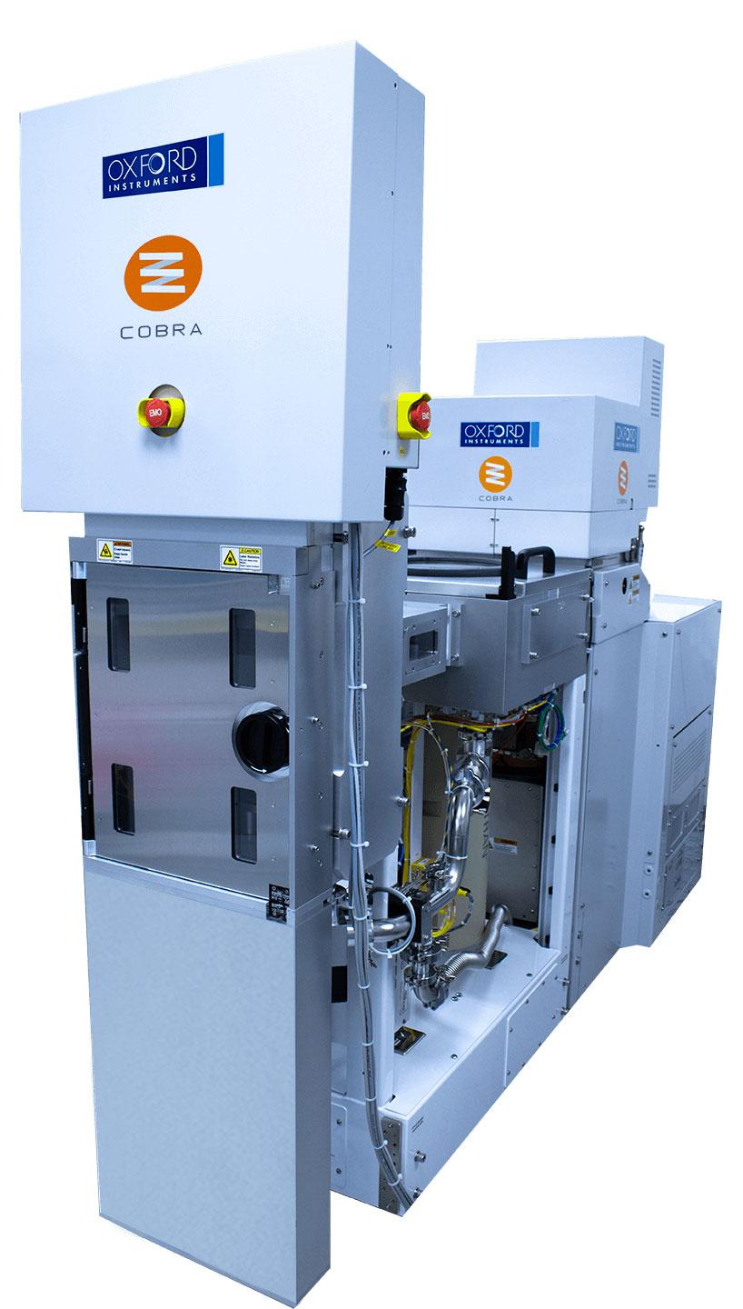
Oxford Instruments Plasma Technology announced May 25, 2021, (LINK) that a leading German semiconductor manufacturer to the automotive industry has selected its PlasmaPro®100 Cobra® system for the development of next generation GaN power electronic devices.
The PlasmaPro®100 Cobra® system is designed for superior uniformity, high- precision and low-damage process solutions. The production-proven system allows for rapid change between wafer sizes up to 200 mm and the cost of ownership is one of the lowest in the market.
The PlasmaPro®100 Cobra® system will be incorporated into the R&D section and will be used for development of GaN power devices. GaN power devices are gaining market share in fast charger applications and offer benefits in Electric Vehicle power management systems.
We continue to see very encouraging signals in the form of increasingly proactive customer engagement and clear market preparation and positioning activities from significant industry players for the emerging Wide Band Gap power electronic market.
"Our Atomic Scale Processing etch solution being selected by this world leading manufacturer for their GaN power electronics programme is an important strategic win for Oxford Instruments Plasma Technology" comments Klaas Wisniewski, Plasma Technology’s Strategic Business Development Director, who also added: "The GaN based power electronic market is very dynamic with improvements to both performance and cost expected at each design iteration.. This reiterates the importance of our strategy to focus on atomic scale processing solutions such as atomic layer deposition (ALD) and atomic layer etching (ALE). We are pleased that such a leading automotive semiconductor company recognizes the benefits our solutions deliver.
The PlasmaPro 100 ALE delivers precise process control of etching for next-generation semiconductor devices. Specially designed for processes such as recess etching for GaN HEMT applications and nanoscale layer etching, the system's digital/cyclical etch process offers low damage, smooth surfaces.
Digital/Cyclical etch process – etching equivalent of ALD
Low damage
Smooth etch surface
Superb etch depth control
Ideal for nanoscale layer etching (e.g. 2D Materials)
As the transistor gave rise to the information age, quantum technology has the potential to be the next great leap forward. Quantum technology is the application of quantum physics for real-world applications, such as quantum computing, sensing, navigation and communication.
Conventional methods for depositing superconductors include sputtering, pulsed laser deposition (PLD), and chemical vapour deposition (CVD). However, these methods can suffer from drawbacks including a lack of thickness control, poor uniformity and high impurity content.
Atomic layer deposition (ALD) is much more beneficial for thin-film deposition due to its ability to produce films with high purity, precise thickness control, conformal coating in high aspect ratio structures, and uniformity over large-area substrates.
Oxford Instruments Plasma Technology (OIPT) has today launched a revolutionary plasma Atomic Layer Deposition (ALD) high volume manufacturing (HVM) solution delivering a step change needed to address fundamental challenges in the GaN power device industry.
Gallium nitride devices are enabling the next generation of efficient power electronic devices for applications such as compact consumer power supplies, 5G networks, electric vehicles and renewable energy conversion.
GaN devices are more efficient and higher performance than current technologies, however there are manufacturing yield and scalability challenges. These need to be addressed to deliver reliable devices at a competitive cost.
One of the key challenges is a consistently high-quality gate passivation, Atomfab delivers this solution with high throughput and low Cost of Ownership (CoO).
Performance: Excellent passivation and dielectric properties enable the demanding device performance critical for key applications.
Plasma: Remote plasma delivers a reproducible GaN interface. Atomfab precisely controls the plasma to protect the underlying sensitive GaN substrate.
Pace: High throughput delivered by a high deposition rate process on a high uptime HVM platform specifically developed for GaN power applications.
The significantly reduced cost per wafer that Atomfab delivers is enabled by numerous technical innovations including a patent pending revolutionary fast remote plasma source.
Atomfab fulfils the customer needs on a single wafer platform with SEMI standard cluster configurations and improved process controls for the latest compound semiconductor solutions.
“Atomfab provides many key benefits to our GaN device manufacturing customers including significant CoO reduction, increased yield and excellent film quality & device performance. For many years Oxford Instruments Plasma Technology has been known as the go to supplier for compound semiconductor plasma solutions. We’ve leveraged that knowledge onto a HVM platform to ensure optimum devices are produced all day, every day”, says Klaas Wisniewski, Strategic Business Development Director, OIPT.
Mike Gansser-Potts, Managing Director, OIPT states: “We’ve been highly commended for our unique plasma ALD solutions and have listened to our HVM customers to take these solutions to the next level. We are happy to announce that Atomfab provides these HVM solutions to our customers”.
[LED Inside, LINK]
Oxford Instruments Plasma Technology (OIPT) announced that it has
worked with Taiwan’s Industrial Technology Research Institute (ITRI) by
providing multiple PlasmaPro 100 systems including both etch and
deposition for ITRI’s Micro LED R&D program.
The
PlasmaPro 100 ICP process solutions are designed to support leading
edge device applications such as Lasers, RF, Power and advanced LEDs.
[Oxford Instruments, LINK] Leading semiconductor equipment solution providers, Oxford Instruments Plasma Technology (a trading name of Oxford Instruments Nanotechnology Tools Limited, Tubney, Oxford, UK) and ULVAC Inc., (Chigasaki, Kanagawa, Japan) are delighted to announce a key collaboration which will bring leading edge deposition and etch technology solutions to GaN and SiC based Wide Band Gap production customers in Japan.
“Oxford Instruments Plasma Technology is excited to be collaborating with ULVAC in order to bring its proven process solutions to the Japanese power and RF markets”, commented Mike Gansser-Potts, Managing Director, Oxford Instruments Plasma Technology. “This relationship, which will begin with ULVAC as our channel partner in Japan, will allow local production customers access to Oxford Instruments’ suite of Atomic Scale Processing solutions”
“This is indeed a very significant collaboration”, confirmed Tetsuya Shimada, General Manager for Advanced Electronics Equipment Division of ULVAC Inc., “Our new collaborator, Oxford Instruments Plasma Technology, has critical process technology and know-how which complements our own capabilities. Combined with our customer support infrastructure this will allow us to provide a complete solution to our Japanese customers.”
Oxford Instruments Plasma Technology’s Atomic Layer Deposition (ALD) and Atomic Layer Etch (ALE) are critical process steps for GaN and SiC based devices to enable functionality and reliable device manufacturing. With the critical know-how and expertise gained over the last ten years in Wide Band Gap applications, Oxford Instruments Plasma Technology is perfectly placed to serve the technology leading Japanese production customers in these markets.
TOKYO – December 12, 2018 – Releasing its Year-End Total Equipment Forecast at the annual SEMICON Japan
exposition, SEMI, the global industry association representing the
electronics manufacturing supply chain, today reported that worldwide
sales of new semiconductor manufacturing equipment are projected to
increase 9.7 percent to $62.1 billion in 2018, exceeding the historic
high of $56.6 billion set last year. The equipment market is expected to
contract 4.0 percent in 2019 but grow 20.7 percent to reach $71.9
billion, an all-time high. [Source: SEMI LINK]
For 2019, SEMI forecasts that South Korea, China, and Taiwan will remain
the top three markets, with all three regions maintaining their
relative rankings. Equipment sales in South Korea is forecast to reach
$13.2 billion, in China $12.5 billion, and in Taiwan $11.81 billion.
Japan, Taiwan and North America are the only regions expected to
experience growth next year. The growth picture is much more optimistic
in 2020, with all regional markets expected to increase in 2020, with
the market increasing the most in Korea, followed by China, and Rest of
World [Source: SEMI LINK]
After
a period of record growth in 2017-18, the semiconductor equipment
industry is expected to face a slowdown in 2019. Logic is strong but
memory is weak, and the trade issues between the United States and China
are a cause for concern. According to a report in Semiengineering (LINK),
heading into 2019, there is a shortfall of 200 mm equipment. The
industry requires from 2,000-3,000 new or refurbished 200 mm tools to
meet fab demand, according to SurplusGlobal. But there are only 500
available 200 mm tools on the market, according to the company. 200 mm
tool prices will remain high. 300 mm tool prices are lower than 200 mm
tool prices these days
For
the ALD OEM market the situation is therefore heating up even though
the. Currently the top 300 mm ALD equipment companies (ASM, TEL, Lam,
Jusung, Wonik IPS, Applied Materials) does not actively support the
market with pure play 200 mm products except for Large Batch Furnaces.
So if you want a 200 mm single wafer ALD tool today you can buy a 300 mm
tool and equip it with 200 mm handling or go to one of the smaller
companies like Picosun, Veeco, Beneq, Oxford Instruments, which all have
200 mm ALD cluster products on the market today.
From
presentation "ALD/CVD applications, equipment and precursors in high
volume manufacturing" at SEMICON Europa 2018, available on SlideShare LINK.
----
Written by Abhishekkumar Thakur and Jonas Sundqvist
[Oxford Instrument News] Oxford Instruments NanoScience is pleased to announce a partnership with the leading European institutions, including renowned research groups from Germany, France, Spain, Finland, and Portugal. The group is led by the Walther-Meißner-Institute (WMI) of the Bavarian Academy of Sciences and Humanities in Garching, Germany on a European project for developing new quantum applications. The collaborative consortium awarded a three million Euro grant from the EU Quantum Flagship Programme, for the proposal on ‘Quantum Microwaves for Communication and Sensing (QMiCS)’.
QMiCS aims at creating a technological basis for improving communication and sensing methods by employing dedicated micro- and nano-structured circuits, made from superconducting materials, cooled down close to absolute zero temperature to generate microwave radiation exhibiting a particular quantum mechanical property called ‘entanglement’. Exploiting entangled microwaves, a prototype quantum local area network cable for distributed quantum computing and a proof of concept for quantum-enhanced radar shall be demonstrated at WMI within the next three years. Oxford Instruments’ role will be to develop a cryogenic link between two ultra-low temperature fridges one provided by Oxford Instruments NanoScience and the other by the WMI to facilitate the microwave communication at very low temperatures. “We are excited at the potential of developing the next generation of quantum technology tools in association with such leading EU researchers in a consortium led by WMI to enable new innovative applications, using the company’s well established and diverse experience in superconducting and cryogen free ultra-low temperatures”, said Ziad Melhem, the Strategic Business Development Manager from Oxford Instruments NanoScience.
Commonly titanium
nitride (TiN) thickness and resistivity wafer fab in-line metrology is based on
ellipsometry and 4-point probe resistivity mapping. Alternative and relatively
slower or more complex methods are X-ray photoelectron spectroscopy
(XPS), X-ray reflectivity (XRR) and X-ray fluorescence (XRFS). TiN thin
films are highly conductive and lose transparency for thicker layers which can
make it challenging to accurately measure the thickness by ellipsometry above
10-20 nm. At about 50 nm layer thickness TiN is non-transparent and has a
bronze color changing to gold for even thicker layers. In the case of resistivity
mapping, 4-point probe is a destructive method leaving scratches from the
needles that penetrates the TiN layer and possibly also damages the underlying
layers and devices.
Atomic
Layer Deposition of TiN on 200 mm wafers
TiN
is used as a metal gate in complementary metal-oxide-semiconductor (CMOS)
technology as it has low resistivity and is compatible with gate dielectrics.
TiN is also deposited as a wear resistant coating, and barrier layer for copper
diffusion due to its chemical and thermal stability. Traditionally TiN was
deposited using physical vapour deposition techniques which suffer from as poor
step coverage in deep contacts and via trenches due to the shadowing effects
especially in high aspect ratio structures.
Atomic
layer deposition (ALD) is a thin film deposition technique which allows for
Å-level control of the film thickness, excellent uniformity, and conformal
coating of high aspect ratio features.
Therefore,
non-destructive characterization of thickness and electrical uniformity across
the entire surface covered by the deposition is critical to ensure the quality
of the final film. Oxford Instruments demonstrate the deposition of conductive
TiN by plasma enhanced ALD with excellent thickness uniformity and collaborate
with das-nano to map the resistivity uniformity using THz
spectroscopy on 200 mm wafers.


%20(1).png)

.jpg)