ASM has launched the PE2O8, a silicon carbide (SiC) epitaxy system designed to enhance power device production with improved yields and reduced costs. The PE2O8 targets key applications in electric vehicles, green energy, and AI data centers, addressing the need for chips with higher power performance in smaller form factors. Its dual-chamber design enables high throughput, process uniformity, and efficient maintenance, while supporting both 6" and 8" wafer processing. With advanced thermal control and recipe transfer capabilities, the PE2O8 system offers high reliability, making it ideal for SiC epitaxy on bare wafers and during chip fabrication.

ASM's PE2O8 is a high-productivity epitaxy system designed for silicon carbide (SiC) applications, enabling the production of power devices with higher yields and lower costs. It plays a crucial role in industries like electric vehicles, green energy, and AI data centers, where chips must meet high power specifications within smaller form factors. The PE2O8 system features dual reactors for easy chamber maintenance, cross-flow hot wall reactors for precise thermal control, and inductive heating for processing 6" and 8" wafers. It ensures process uniformity and recipe transfer from earlier platforms, making it highly reliable and cost-efficient for SiC epitaxy on bare wafers and in power device fabrication.
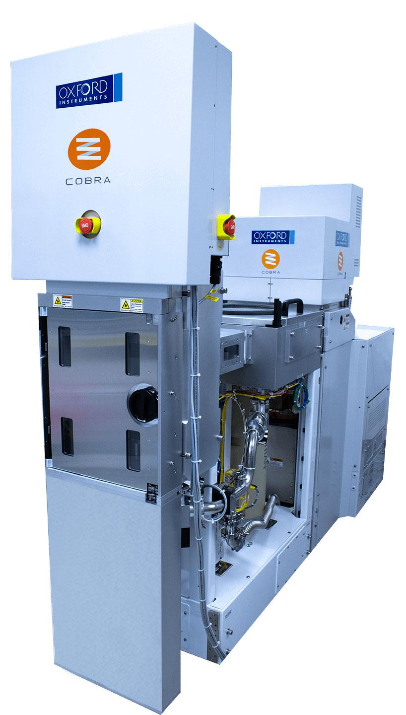
Raleigh, NC, USA, September 30, 2024 / New system extends ASM’s portfolio of industry benchmark single wafer silicon carbide epitaxy systems, the 6” PE1O6 and 8” PE1O8 systems, with a higher throughput, lower cost of ownership, dual chamber, single wafer, 6” and 8” compatible, silicon carbide epitaxy system.
Today at the 2024 International Conference on Silicon Carbide and Related Materials, ASM International N.V. (Euronext Amsterdam: ASM) introduced the PE2O8 silicon carbide epitaxy system, a new, dual chamber, platform for silicon carbide (SiC) epitaxy (Epi). Designed to address the needs of the advanced SiC power device segment, the PE2O8 is the benchmark epitaxy system for low defectivity, high process uniformity, all with higher throughput and low cost of ownership needed to enable broader adoption of SiC devices.
As the general electrification trend drives more power device manufacturers to utilize SiC for a growing number of high-power applications (such as for electric vehicles, green power, and advanced data centers) the expanded demand and requirements for lower cost for SiC is causing a transition from 6” to 8” SiC substrates. At the same time, SiC device manufacturers are designing higher power devices that will benefit from better SiC epitaxy.
Utilizing a unique design, the dual chamber PE2O8 system deposits SiC with ultra precise control, enabling benchmark higher yield and higher throughput. The highly compact, dual chamber design enables high productivity and low total costs of operation. Additionally, the system features an easy preventive maintenance approach helping to increase uptime and reduce the occurrence of unscheduled downtime. System deliveries have been ongoing to multiple customers globally, among them leaders in SiC power device manufacturing.
“We are at a critical inflection for silicon carbide power products, as our customers transition from 6” to 8” wafers”, said Steven Reiter, Corporate Vice President, and business unit head of Plasma and Epi at ASM. “Delivering a high-quality epitaxy process on larger wafers with defectivity control is critical, and we have been the industry benchmark for process uniformity with our novel chamber design. We have now extended our system capability to improve our process control and our value for customers with lower cost of ownership.”
Since 2022, ASM, through its new SiC Epi product unit has been developing and refining its single wafer SiC epitaxy system. With the structurally higher demand for electric vehicles and improvement of the overall SiC wafer and device yield, the equipment market for SiC epitaxy has grown substantially in recent years.
About ASM International
ASM International N.V., headquartered in Almere, the Netherlands, and its subsidiaries design and manufacture equipment and process solutions to produce semiconductor devices for wafer processing, and have facilities in the United States, Europe, and Asia. ASM International's common stock trades on the Euronext Amsterdam Stock Exchange (symbol: ASM). For more information, visit ASM's website at www.asm.com.
Sources:


%20(1).png)


.jpg)