Thursday, January 27, 2022

ALD InGaN with single precursor pulse of In & Ga

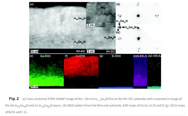
Polla Rouf of Pedersen Group in Linköping Sweden, just published an ALD approach to metastable In1−xGaxN with 0.1 < x < 0.5 based on solid In- and Ga-precursors that were co-sublimed into the deposition chamber in one pulse. A near In0.5Ga0.5N film with a bandgap value of 1.94 eV was achieved on a Si(100) substrate. Epitaxial In1−xGaxN(0002) was successfully grown directly on the 4H–SiC(0001) substrate.

I checked in with Prof. Pedersen on Twitter and this is gonna be one of the abstract submitted to AVS ALD 2022 in Ghent this summer.

  • The sequential pulsing of the precursors in ALD presents a challenge to depositing a homogeneous ternary material as only one precursor can be pulsed into the reactor at a time.
  • Ternary materials are therefore deposited by ALD as stacks of two binary materials. In1−xGaxN could therefore be deposited as layers of InN and GaN in an ABAB⋯CBCB… super-cycle approach where A and C are In- and Ga-precursors, respectively, and B is the N-reactant. By varying the number of cycles for each binary material, the overall composition of the ternary material can be tuned. 
  • This approach relies on diffusion of the two binary materials to form a homogeneous ternary phase. Otherwise, a multilayer of InN/GaN is obtained. This ALD approach has been used to obtain In1−xGaxN with x ranging from 0.15–0.85 using trimethylindium and trimethylgallium.
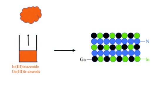
  • Here, an alternative method to depositing ternary materials by introducing both metal precursors with a single pulse. This renders mixing of the metals in both the growth direction and in the growth plane. This was achieved by mixing and co-subliming two solid metal precursors into the ALD chamber.


Wednesday, January 26, 2022

AVS Seminar Atomic Layer Deposition from an Applications Perspective by Prof. Kessels

 Coming up soon - AVS Seminar Atomic Layer Deposition from an Applications Perspective by Prof. Kessels, TU Eindhoven.

Read about the background at AtomicLimits LINK.

Atomic Layer Deposition from an Applications Perspective

February 9, 2022
1:00 PM - 5:00 PM
Instructor(s): Erwin Kessels
REGISTER HERE!

Questions? Contact Heather Korff, heather@avs.org, 530-896-0477


Cover image - ALD Applications from AtomicLimits.com. Schematic overview of the (emerging) industrial applications of atomic layer deposition (ALD). Roughly speaking three main areas can be distinguished: those related to (opto)electronic integrated circuits (blue); those related to large area electronics and energy technologies (red) and other applications (green) that are often in niche markets. The layout of the figure is inspired by a figure posted on the Strem Chemicals website (by BALD Engineering AB). A high-resolution version of this figure can be found in the AtomicLimits Image Library.


Monday, January 24, 2022

BENEQ gives insights to the growing USD 345 Million More than Moore market for ALD Equipment

Here is an insightful interview with Patrick Rabinzohn, Ph.D., VP of the Semiconductor ALD Business Unit at Beneq regarding ALD in the More than Moore market (MtM) LINK. Yole Development recently release a report on the topic as summarized below.

Atomic Layer Deposition (ALD) is known in the electronics industry as an enabler for the scaling of logic and memory semiconductor devices. Ultimately, this scaling leads to performance improvement of devices such as dynamic random-access memory (DRAM), advanced fin field effect transistor (FinFET) and Gate All Around transistors. ALD is now percolating into More-than-Moore (MtM) device production, again enabling novel architectures, materials, and performance improvements. Examples include GaN and SiC transistors, in particular GaN High Electron Mobility Transistors (HEMTs) and SiC trench metal oxide semiconductor FETs (MOSFETs), piezoelectric microelectromechanical systems (MEMS) and radiofrequency (RF) devices or compound semiconductor mini-light emitting diodes (LEDs) and micro-LEDs.

Besides the technical benefits that ALD offers, surging ALD equipment sales are propelled by fab capacity expansions worldwide. Forecasts expect the ALD equipment market for MtM devices to grow in the coming years with a 12% Compound Annual Growth Rate from 2020-2026 (CAGR2020-2026) reaching $680.5M in 2026.
You can find detailed know-how, market, and ecosystem overview of ALD equipment dedicated to MtM device production in the technology and market report Atomic Layer Deposition Equipment for More than Moore 2021, published by Yole Développement (Yole). Among the featured equipment manufacturers, Beneq is gaining momentum in the MtM space with a rapidly growing equipment lineup.

Picosun part of extensive quantum technology 10 Million Euro QuTI project is coordinated by VTT Technical Research Centre of Finland

ESPOO, Finland, 18th of January 2022 – Picosun takes part as an industrial partner in QuTI, a recently launched extensive research project aiming to develop new components, manufacturing and testing solutions that are needed in quantum technology. Quantum technology has gained interest in a vast array of industries on a large scale. The remarkable performance improvements it offers enable for example powerful computing and benefits in communications, healthcare, sensors, imaging and measurement applications.


The QuTI project is coordinated by VTT Technical Research Centre of Finland, and it has a total budget of around 10 million euros. Other industrial partners of the consortium include Bluefors, Afore, IQM, Rockley Photonics, CSC, Quantastica, Saab and Vexlum. The research partners are VTT, Aalto University and the University of Tampere.

“Quantum technology is a multidisciplinary and rapidly advancing field. The QuTI consortium provides an ideal starting point for strengthening the international competitiveness of Finnish technology and industry in this fast-growing field,” says QuTI project’s coordinator, Research Professor Mika Prunnila from VTT.

“Quantum technology has already taken the step from research laboratories to commercial applications. We look forward in supporting this development trend even further and being part of creating a globally competitive industrial ecosystem in Finland around this technology,” says Dr. Jani Kivioja, CTO of Picosun Group.

“Atomic Layer Deposition, or ALD, is the advanced thin film coating method for ultra-thin, highly uniform and conformal material layers that enables the digital solutions of today. It will also play a crucial role in future innovations and in the quantum computing, communication and sensing devices that will be developed in the QuTI project”, continues Jussi Rautee, CEO of Picosun Group.


More information:
Jani Kivioja
CTO, Picosun Group
Tel: +358 46 922 8804
Email: info@picosun.com

Picosun provides the most advanced ALD (Atomic Layer Deposition) thin film coating solutions for global industries. Picosun’s ALD solutions enable technological leap into the future, with turn-key production processes and unmatched, pioneering expertise in the field – dating back to the invention of the technology itself. Today, PICOSUN® ALD equipment are in daily manufacturing use in numerous leading industries around the world. Picosun is based in Finland, with subsidiaries in Germany, USA, Singapore, Japan, South Korea, China mainland and Taiwan, offices in India and France, and a world-wide sales and support network. Visit www.picosun.com.


Friday, January 7, 2022

TSMC Self-Aligned Via Process Development for Beyond the 3nm Node

Semiwiki Tom Dillinger reports on an interesting paper by TSMC at the recent IEDM 2021 conference in San Francisco using selective ALD with the help of SAMs or Dielectric on Dielectric (DOD) as it is called.


From the article sumary: Continued interconnect scaling below the 3nm node will necessitate unique process development research to maintain electrical and reliability specs in the presence of (up to 4nm) overlay error. The need for low-K interlevel dielectrics is a given – yet, the via etch in these materials is not especially tolerant of EPE.

TSMC has demonstrated a potential process flow for a “self-aligned via” with an additional DoD material. The etch rate differential of the DoD results in more robust via-to-adjacent metal reliability. This process flow utilizes two unique steps – the SAM of a blocking material on metal surfaces, and the selective ALD of a dielectric-on-dielectric.