Showing posts with label GaN. Show all posts

Tuesday, March 19, 2024

Laser Slicing Technique Revolutionizes GaN Substrate Recycling, Paving the Way for Cost-Effective Vertical Power MOSFETs

A study led by Takashi Ishida and colleagues explored a recycling process for gallium nitride (GaN) substrates using a laser slicing technique, aiming to reduce the cost of GaN vertical power MOSFETs. GaN is noted for its potential in high-power applications due to its superior electrical properties compared to silicon. The cost of GaN devices, while expected to be lower than silicon carbide (SiC) devices, is significantly impacted by the expensive GaN substrates. The proposed recycling process involves the use of laser slicing to separate used GaN substrates into thin device chips and a remaining substrate portion, which can then be smoothed, polished, and reused for further device fabrication.


The research demonstrated that the electrical properties of devices fabricated on recycled GaN substrates, specifically lateral MOSFETs and vertical PN diodes, showed no degradation compared to those on new substrates. This indicates that the recycling process does not adversely affect the substrate's quality or the performance of subsequent devices. The study's findings suggest that this recycling method could be a viable strategy to lower the production costs of GaN-based power devices, potentially facilitating their broader adoption in high-power applications.


Source: Demonstration of recycling process for GaN substrates using laser slicing technique towards cost reduction of GaN vertical power MOSFETs - IOPscience

Tuesday, February 6, 2024

Powering the Future: The Rise of Compound Semiconductor Substrates and Epiwafers

Yole Group reports that the compound semiconductor substrate market is on the brink of a significant transformation, poised to reach a staggering US$3.3 billion by 2029, with an impressive compound annual growth rate of 17% from 2023 to 2029. This growth is underpinned by the relentless innovation and strategic foresight of leading players like Wolfspeed and Coherent, who are continuously refining their product portfolios and expanding their market footprints.

Atomic Layer Deposition (ALD) and Atomic Layer Etching (ALE) play specific roles in the compound semiconductor industry. ALD is used to apply ultra-thin layers crucial for semiconductor devices, especially in insulating layers and gate dielectrics in transistors. ALE, with its precise etching capability, is key for crafting fine details in devices, often used in the patterning of nanoscale structures in LEDs and high-frequency transistors. These technologies support the development of advanced, reliable applications in power electronics and photonics.

At the heart of this industry evolution are the advancements in compound semiconductor technologies, spanning materials such as Silicon Carbide (SiC), Gallium Nitride (GaN), and Indium Phosphide (InP). These materials are catalyzing a revolution across various sectors, with SiC leading the charge in the automotive industry, particularly within the burgeoning 800V electric vehicle segment. GaN, on the other hand, is making inroads into consumer electronics and automotive applications, promising to redefine power electronics with its superior efficiency.

Check link below for High-Res graph

The impact of compound semiconductors extends beyond power electronics into the realm of photonics, where InP and GaAs are setting new benchmarks. InP, for instance, is witnessing a resurgence, driven by its critical role in AI applications, while GaAs photonics continues to grow, albeit at a steadier pace.

Yole Group, a market research and strategy consulting firm, in its latest "Status of Compound Semiconductors Industry 2024" report, provides an exhaustive analysis of these trends. The report delves into each substrate's market dynamics and technological advancements, offering a comprehensive overview of the ecosystem.

LINK: Compound semiconductors industry: an unprecedented promise (yolegroup.com)

As the industry stands at the precipice of transitioning to larger diameter substrates, the demand for high-data-rate lasers in AI is pushing for a shift to 6” InP substrates. Concurrently, GaAs is exploring the potential of 8” manufacturing for MicroLEDs, despite the challenges it faces against OLED technology.

In this dynamic landscape, companies like Wolfspeed and Coherent are not just participants but are leading the charge towards a more efficient, technologically advanced future. Their efforts in expanding material capacity and forging strategic alliances are testament to the industry's readiness to embrace the next wave of semiconductor innovation.


Friday, November 24, 2023

Oxford Instruments Secures Major Orders for GaN ALE & ALD Systems from Leading Japanese Power Electronics and RF fabs

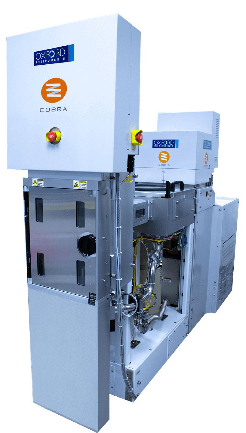
Oxford Instruments has received significant orders for its GaN ALE (Atomic Layer Etch) and ALD (Atomic Layer Deposition) systems from major Japanese foundries specializing in power electronics and RF (Radio Frequency). These systems are essential for producing GaN (Gallium Nitride) HEMT (High Electron Mobility Transistor) devices, catering to rapidly growing markets such as consumer fast-charging, data centers, and 5G/6G communications.


Oxford Instruments Plasma Technology staff at ALD2018/ALE2018 in Korea (Looking Back on ALD/ALE 2018 - Oxford Instruments (oxinst.com))

The company's ALD technology is known for its high throughput and low damage plasma processing, enhancing film and interface quality. It is widely used by leading GaN HEMT device manufacturers globally. The ALE solution, particularly for p-GaN HEMTs, is production-qualified and offers precise etching with minimal damage, featuring Etchpoint®, a unique endpoint detection technology developed in collaboration with LayTec AG.


Atomic Scale Processing

Etchpoint® allows for automated transition from standard high-rate etching to low damage ALE, improving device reliability. It enables precise AlGaN recess etches, crucial for the next generation GaN MISHEMT E-mode devices, with an accuracy of ±0.5 nm. These technologies can be integrated into an automated handler for multi-chamber processing without breaking vacuum, enhancing device performance and yield at a lower cost.


Gallium Nitride (GaN) provides higher breakdown strength, faster switching speed, and higher thermal conductivity for power electronics and RF applications. To support the high-volume manufacture of reliable GaN HEMT devices, Oxford Instruments in collaboration with LayTec have developed and optimised a new etch-depth monitoring solution to reliably fabricate GaN HEMT device structures. PlasmaPro 100 ALE with Etchpoint® system provides low damage etching with surface smoothing with unparalleled accuracy in target etch depth for devices such as p-GaN HEMTs and recessed gate MISHEMTs. Etchpoint is fully integrated with both the hardware and software of the PlasmaPro 100 ALE system, offering unrivalled accuracy of etch layer depth for GaN and AlGaN.

Dr. Aileen O'Mahony, GaN Product Manager at Oxford Instruments Plasma Technology, highlighted the significance of these orders from Japan, emphasizing the optimization of their ALD solution for GaN-surface plasma pre-treatment and the implementation of ALE with Etchpoint®. These developments are crucial in addressing complex challenges in device manufacturing while ensuring high throughput, reliability, and uptime in production.


Wednesday, November 22, 2023

AIXTRON's G10-GaN System Empowers BelGaN's Expansion into the Growing GaN Semiconductor Market

The article discusses AIXTRON's support for BelGaN in expanding its Gallium Nitride (GaN) business through the new G10-GaN system. AIXTRON SE, a semiconductor company, is enabling BelGaN, a leading GaN automotive-qualified semiconductor foundry in Europe, to enter the growing GaN market and boost GaN technology innovation. BelGaN plans to use AIXTRON's G10-GaN, which offers top performance, a compact design, and low cost per wafer, starting with an 8x150mm configuration, to be delivered to BelGaN's production site in Oudenaarde, Belgium, by the end of 2023. This system will later evolve to support 5x200mm.


AIXTRON's G10-GaN System Empowers BelGaN's Expansion into the Growing GaN Semiconductor Market

BelGaN aims to expand its power chip range with voltage ratings from 40V to 1200V, utilizing GaN-on-Si, GaN on SOI, and new GaN-on-engineered substrates, focusing on high performance, automotive quality, reliability, high yield, and low costs. The G10-GaN will enable innovations in device architectures and improvements in performance, yield, and quality, reducing the cost of GaN products. This advancement is expected to drive growth in e-mobility, datacom, energy conversion, and contribute to a carbon-neutral society.


The G10-GaN epitaxy system is a highly efficient, productive, and cost-effective solution for GaN power and RF applications, combining single wafer performance with the economy of batch processing.

Dr. Marnix Tack of BelGaN praised the productivity, uniformity, and low cost of ownership of the G10-GaN, while Dr. Felix Grawert of AIXTRON expressed pride in BelGaN's choice of their technology. The G10-GaN, building on the G5+ C platform, offers double the productivity per cleanroom area, better material uniformities, and over 25% lower cost of ownership compared to other market equipment, making it a competitive choice for AIXTRON's customers. This MOCVD system is fully automated and designed for silicon fabs, marking a significant technological step in the semiconductor industry.

G10 GaN Performance (www.aixtron.com)

The G10-GaN by AIXTRON is a state-of-the-art deposition system for 150/200 mm GaN epitaxy, designed for GaN power and RF applications. It features a compact cluster design with three process chambers, reducing the footprint by 50% while maximizing wafer yield per square meter. This system significantly improves device yield with a threefold increase in on-wafer uniformity and maintains low particle levels, enhancing overall quality and consistency.

Cost-effectiveness is a key attribute, with the G10-GaN offering more than 25% lower epitaxial cost per wafer compared to other platforms. It incorporates Planetary Reactor® technology for high wafer yield and uniformity. The system's productivity is marked by over 90% equipment uptime and highest throughput per fab area, supported by features like fully automated wafer handling and advanced temperature control.

The G10-GaN ensures easy maintenance and operation with features like automated chamber cleaning and predictive functionalities. It's compatible with existing AIX G5+ C tools, facilitating seamless process transfers. Overall, the G10-GaN epitaxy system combines efficiency, cost-effectiveness, and advanced technology, making it an optimal choice for semiconductor manufacturing in the GaN sector.

Market opportunity for GaN for MOCVD and ALD


ALD and MOCVD is rapidly gaining traction in the semiconductor industry, particularly for logic, memory, and wide-bandgap power semiconductors. This growth is highlighted by industry experts at SEMICON Europa 2023. ALD is primarily adopted for its excellent surface passivation qualities, essential in GaN power electronic devices. While miniaturization drives ALD use in some sectors, its primary role in power electronics is to provide high-quality, conformal coatings, crucial for device performance and reliability. Thermal ALD processes like Al2O3 and AlON are key for GaN transistors, offering improved interface layers for low dynamic switching losses. ALD's impact is most notable in consumer, automotive, and industrial markets, where it enhances device performance and longevity. Looking forward, continued optimization of ALD processes and in-situ surface treatments are expected to further enhance device performance and reliability, especially in GaN power electronic devices, with high growth predicted in various end markets.


Tuesday, November 21, 2023

Revolutionizing Power Technology: Intel's Integrated CMOS Driver-GaN (DrGaN) Power Switch for Enhanced Efficiency and Density in Data Centers and Networks

Intel researchers have developed an integrated CMOS Driver-GaN (DrGaN) power switch, combining gallium nitride (GaN) and silicon CMOS technologies on a 300mm GaN-on-Si platform. This innovation is designed to meet the increasing power density and efficiency needs of data centers and networking platforms. The new device, termed DrGaN, features an e-mode HEMT and an integrated 3D monolithic Si PMOS. It's capable of addressing the power requirements of future CPUs and GPUs, showing excellent resistance and leakage performance. A key advancement is the development of a new gate-last process flow for 3D monolithic integration of GaN and Si CMOS through layer transfer. 


Intel researchers have developed an integrated CMOS Driver-GaN (DrGaN) power switch, combining gallium nitride (GaN) and silicon CMOS technologies on a 300mm GaN-on-Si platform.

This process involves completing the high-temperature activation steps for the Si CMOS transistors before depositing the GaN transistor's gate dielectric, solving a major challenge in integrating these two technologies. This method also allows GaN and Si CMOS transistors to share the same backend interconnect stack, which reduces resistance and mask count. The new technology demonstrates great promise for scaling, evidenced by a figure of merit of 0.59 (mΩ-nC)-1 for a 30nm gate-length GaN MOSHEMT. The paper includes images of the new process flow, the 3D monolithic integration, and the layout of a DrGaN unit cell, illustrating the advanced integration and circuitry of this novel power device.

Wednesday, October 25, 2023

Infineon Acquires GaN Systems for $830M, Bolstering Position in Power Semiconductor Market

Strategic Move Amplifies Infineon's GaN Expertise, Accelerating Energy-Efficient Solutions and Decarbonization Efforts

Infineon Technologies has successfully acquired GaN Systems, a Canadian company, for $830 million. This acquisition positions Infineon as a significant supplier of gallium nitride (GaN) power devices across various sectors, including consumer, industrial, and automotive applications. With the deal, Infineon inherits a wide array of GaN-based power conversion devices, designs, and advanced application expertise. GaN Systems, located in Ottawa, has integrated with Infineon, which already had its CoolGaN range. Jochen Hanebeck, Infineon's CEO, emphasized that GaN technology promotes energy efficiency and contributes to decarbonization efforts. Following this acquisition, Infineon boasts 450 GaN experts and access to over 350 GaN patent families, solidifying its leadership in the power semiconductor domain. The collaboration of both companies' intellectual properties, application insights, and customer projects optimally positions Infineon for future growth. 

Notably, GaN Systems has a unique island-based device structure that enhances power design performance, utilized by companies like QPT for fast switching speeds of up to 20MHz. This acquisition comes after Infineon's 2020 purchase of Cypress Semiconductor.

Source: Infineon completes acquisition of GaN Systems ... (eenewseurope.com)

Thursday, September 7, 2023

AIXTRON Unveils G10-GaN Cluster Solution for Power Electronics Market

AIXTRON SE has unveiled the G10-GaN cluster solution for high-volume manufacturing of Gallium Nitride (GaN) power and RF devices. The platform delivers superior performance, a compact design, and cost-efficiency. Dr. Felix Grawert, CEO of AIXTRON, highlighted its potential in reducing global CO2 emissions and its growing demand in applications like mobile fast chargers, data centers, and solar energy. The system improves material uniformity, extends equipment uptime, and offers a 25% cost reduction per wafer, making it a significant advancement in semiconductor technology.

Herzogenrath, September 6, 2023 – AIXTRON SE, the semiconductor industry's leading deposition equipment supplier, has introduced its latest innovation, the G10-GaN cluster solution for Gallium Nitride (GaN) based power and radio frequency (RF) devices. This groundbreaking platform is making its debut at SEMICON Taiwan (September 6-8, 2023) in Taipei, offering unparalleled performance, a compact design, and exceptional cost-efficiency.

The cluster can be equipped with up to three process modules, delivering a record capacity of 15x200 mm wafers thanks to Planetary batch reactor technology – enabling a 25 percent cost reduction per wafer compared to previous products. LINK

Dr. Felix Grawert, CEO and President of AIXTRON SE, proudly announced, "Our new G10-GaN platform has already received qualification for high-volume production of GaN Power devices from a prominent US device manufacturer. It delivers double the productivity per cleanroom area compared to our previous product, enhances material uniformity, and provides a competitive edge to our customers."

GaN-based technologies are gaining importance in the drive to reduce global CO2 emissions due to their significantly more efficient power conversion capabilities compared to traditional silicon (Si). GaN can reduce power losses by a factor of two to three. Dr. Grawert noted, "We anticipate continuous growth in the GaN market throughout this decade and beyond. GaN has already replaced silicon in fast chargers for mobile devices, and we are witnessing rising demand in data centers and solar applications."

AIXTRON has been at the forefront of GaN on Si process and hardware development for over two decades. The company's AIX G5+ C planetary reactor, known for being the first fully automated GaN Metal-Organic Chemical Vapor Deposition (MOCVD) system with In-Situ Cleaning and Cassette-to-Cassette automation, is now an industry-standard tool for GaN power production. The new G10-GaN cluster solution builds upon this legacy, elevating every performance metric.

Designed to maximize cleanroom space, the G10-GaN features innovative reactor inlets that enhance material uniformity, resulting in optimized device yields. The platform incorporates on-board sensors, a new software suite, and fingerprint solutions to ensure consistent performance across runs, even between maintenance cycles, extending equipment uptime by over 5% compared to the previous generation.

The cluster can accommodate up to three process modules, boasting a record capacity of 15x200 mm wafers thanks to Planetary batch reactor technology. This enables a remarkable 25% reduction in cost per wafer compared to previous products, a factor that promises significant savings for manufacturers.

AIXTRON's G10-GaN cluster solution positions the company as a key player in the ever-evolving landscape of GaN-based power and RF devices, furthering its commitment to advancing semiconductor technology for a sustainable future.

Thursday, September 22, 2022

Oxford Instruments and ITRI report GaN HEMT device performance by ALD and ALE

GaN HEMT device performance - Oxford Instruments and ITRI announce breakthrough development in GaN HEMT device performance


Oxford Instruments alongside its research partner Industrial Technology Research Institute (ITRI) can today share new and exciting technology developments that will significantly benefit key hyper-growth electric vehicle, datacentre and 5G markets. The technology developments allow critical transistor components to operate at higher voltages which increases performance and reliability, while also achieving a safer and more energy efficient (normally off ‘E-mode’) operation compared to existing devices. The new GaN (gallium nitride) HEMT device architecture is defined by a recessed and insulated gate junction into the AlGaN layer, and this device is referred to as GaN MISHEMT.

In September 2021, Oxford Instruments Plasma Technology and ITRI announced a cooperative research program for next-gen compound semiconductors. This latest breakthrough is an example of that collaboration delivering on its goal of accelerating technology to benefit the partners, their regions and wider global markets. Since that announcement, Oxford Instruments has also unveiled an exclusive supply deal with Laytec, who’s endpoint technology is used to control the GaN MISHEMT recess gate depth. Recess depth accuracy and repeatability is critical to tune the device performance characteristics, and LayTec’s technology is designed specifically for this application achieves target depth accuracy of ±0.5nm. ITRI provides pilot production and value-added services, including process verification and product development. ITRI’s integration services, especially this GaN development project, have proved incredibly beneficial, which quickly proved out the higher performance of GaN MISHEMT and provided a lower risk and faster route to market for the device.

Klaas Wisniewski, Oxford Instruments Strategic Business Development Director commented: “We have excellent strategic partners and customers like Enkris, ITRI, LayTec and ROHM, and our GaN solutions are positioned strongly to serve, grow and gain from big opportunity markets. Our leading Atomic Layer Etch (ALE) and Atomic Layer Deposition (ALD) technology is raising material engineering performance to achieve new levels of surface quality and defect reduction, to meet the growing demand for higher performing devices.” Klaas also added: “With our technology partner ITRI, high volume GaN manufacturing customers and our focussed investment into high value and proprietary process solutions, we expect the GaN device market to be a key driver for our business and technology roadmap.”

Klaas Wisniewski presented a talk entitled “Enhancing GaN HEMT Performance for Power Electronics Applications with Atomic Scale Processing Production Solutions” at Semicon Taiwan Sept 14-16, 2022, TaiNEX 1, Taipei, Taiwan. Please get in touch with us to discuss our latest data and opportunities for partnership and collaboration.

Wednesday, August 31, 2022

Equipment Suppliers Brace For GaN Market Explosion - including Atomic Layer Etch (ALE)

According to a recent article in Semiengineering Power Electronics and RF will drive volume for equipment suppliers, with many new uses underway. According to industry experts interviewed, also ALD and ALE will benefit

“Through an ongoing development program, Lam Research has been establishing a suite of enabling process solutions for GaN semiconductor device fabrication,” said David Haynes, vice president of specialty technologies in Lam Research’s Customer Support Business Group. 

“Key to these capabilities is an atomic layer etch-based process that can provide ultra-low damage, atomic scale precision etching of GaN and related materials. The new, optimized processes can reduce the post etch sheet resistance of the as-etched GaN/AlGaN [aluminum gallium nitride] whilst the surface roughness of the etched material remains comparable to that of the incoming epitaxial layers. Such high-precision, low-damage etch capabilities are critical to the formation of p-GaN or recessed gate high electron mobility transistor (HEMT) architectures used to fabricate normally off GaN devices for power electronics applications.”


Lam’s Kiyo45 reactive ion etch (RIE) tool offering ALE processes of GaN and SiC materials Source: Lam Research

According to the article, Lam has developed proprietary solutions to speed up the ALE process and its ALE chambers can be used in both RF and power GaN fabrication.

Lam sees GaN on SiC RF devices as well established and will remain very important for high power applications in telecommunications infrastructure and defense. Fast development of GaN-on-Si epitaxy will move towards high volume applications for consumer products according to Haynes and explained further: “These will evolve alongside GaN-on-Si power devices that share many of the same process challenges. Today, most GaN-on-SiC RF devices are still made on 150mm or even 100mm wafers. The opportunity for GaN-on-Si devices to be readily processed on 200mm and in the future 300mm wafers, as well as the potential to use complementary metal-oxide semiconductor (CMOS) foundry capacity and even develop integrated solutions with CMOS, will all be key drivers for this transition.”

The Lam Research was early in high volume manufacturing with ALE (2016 BALD Engineering - Born in Finland, Born to ALD: Lam Research - New Atomic Layer Etching Capability Enables Continued Device Scaling) ALE chambers are now also part of their Kyo45 reactive ion etch product platform and offers (lamreserch.com):
  • Superior uniformity and repeatability enabled by a symmetrical chamber design, industry-leading electrostatic chuck technology, and independent process tuning features
  • High productivity with low defectivity on multi-film stacks enabled by in-situ etch capability, continuous plasma, and advanced waferless auto-clean technology
  • Improved critical dimension uniformity using proprietary Hydra® technology that corrects for incoming patterning variability
  • Corvus® plasma sheath tuning for maximum yield of wafer-edge dies
  • Atomic-scale variability control with production-worthy throughput enabled by plasma-enhanced ALE capability
  • Upgradable products for low cost of ownership over several device generations
Sources: 

- Equipment Suppliers Brace For GaN Market Explosion

- Lam Research www.lamresearch.com

Wednesday, September 15, 2021

Problem solved - In0.5Ga0.5N layers by Atomic Layer Deposition!

Pedersen Group at Linköping University, Sweden, present an ALD approach to metastable In1-xGaxN with 0.1 < x < 0.5 based on solid In- and Ga-precursors that were co-sublimed into the deposition chamber in one pulse. A near In0.5Ga0.5N film with a bandgap of 1.94 eV was achieved on Si (100) substrate. Epitaxial In1-xGaxN (0002) was successfully grown directly on 4H-SiC (0001).

In0.5Ga0.5N layers by Atomic Layer Deposition
P. Rouf, J. Palisaitis, B. Bakhit, N. J. O'Brien and H. Pedersen, J. Mater. Chem. C, 2021, DOI: 10.1039/D1TC02408F. (LINK)


a) Cross-sectional STEM-HAADF image of the ~60 nm In1-xGaxN film on 4H-SiC substrate with a zoomed in image of the b) In82Ga18N and c) In18Ga82N layers. d) SAED pattern from the film and substrate. EDX maps of Ga e), In f) and Si g). EELS maps of N h) and C i).

Wednesday, May 5, 2021

Imec and AIXTRON Demonstrate 200 mm GaN Epitaxy on AIX G5+ C

Imec and AIXTRON Demonstrate 200 mm GaN Epitaxy on AIX G5+ C for 1200V Applications with Breakdown in Excess of 1800V

LEUVEN (Belgium), APRIL 29, 2021 — Imec, a world-leading research and innovation hub in nanoelectronics and digital technologies, and AIXTRON, the leading provider of deposition equipment for compound semiconductor materials, have demonstrated epitaxial growth of gallium-nitride (GaN) buffer layers qualified for 1200V applications on 200mm QST® substrates, with a hard breakdown exceeding 1800V. The manufacturability of 1200V-qualified buffer layers opens doors to highest voltage GaN-based power applications such as electric cars, previously only feasible with silicon-carbide (SiC)-based technology. The result comes after the successful qualification of AIXTRON’s G5+ C fully automated metal-organic chemical vapor deposition (MOCVD) reactor at imec, Belgium, for integrating the optimized material epi-stack.

AIX G5+ C reactor module with cassette-to-cassette wafer handler (www.aixtron.com)

Wide-bandgap materials gallium-nitride (GaN) and silicon-carbide (SiC) have proved their value as next-generation semiconductors for power-demanding applications where silicon (Si) falls short. SiC-based technology is the most mature, but it is also more expensive. Over the years tremendous progress has been made with GaN-based technology grown on for example 200mm Si wafers. At imec, qualified enhancement mode high-electron-mobility transistors (HEMTs) and Schottky diode power devices have been demonstrated for 100V, 200V and 650V operating voltage ranges, paving the way for high-volume manufacturing applications. However, achieving operating voltages higher than 650V has been challenged by the difficulty of growing thick-enough GaN buffer layers on 200mm wafers. Therefore, SiC so far remains the semiconductor of choice for 650-1200V applications – including for example electric cars and renewable energy.

For the first time, imec and AIXTRON have demonstrated epitaxial growth of GaN buffer layers qualified for 1200V applications on 200mm QST® (in SEMI standard thickness) substrates at 25°C and 150°C, with a hard breakdown exceeding 1800V. Denis Marcon, Senior Business Development Manager at imec: “GaN can now become the technology of choice for a whole range of operating voltages from 20V to 1200V. Being processable on larger wafers in high-throughput CMOS fabs, power technology based on GaN offers a significant cost advantage compared to the intrinsically expensive SiC-based technology.”

Key to achieving the high breakdown voltage is the careful engineering of the complex epitaxial material stack in combination with the use of 200mm QST® substrates, executed in scope of the IIAP program The CMOS-fab friendly QST® substrates from Qromis have a thermal expansion that closely matches the thermal expansion of the GaN/AlGaN epitaxial layers, paving the way for thicker buffer layers – and hence higher voltage operation.

Dr. Felix Grawert, CEO and President of AIXTRON “The successful development of imec’s 1200V GaN-on-QST® epi-technology into AIXTRON’s MOCVD reactor is a next step in our collaboration with imec. Earlier, after having installed AIXTRON G5+C at imec’s facilities, imec’s proprietary 200mm GaN-on-Si materials technology was qualified on our G5+ C high-volume manufacturing platform, targeting for example high-voltage power switching and RF applications and enabling our customer to achieve a rapid production ramp-up by pre-validated available epi-recipes. With this new achievement, we will be able to jointly tap into new markets.” Currently, lateral e-mode devices are being processed to prove device performance at 1200V, and efforts are ongoing to extend the technology towards even higher voltage applications. Next to this, imec is also exploring 8-inch GaN-on-QST® vertical GaN devices to further extend the voltage and current range of GaN-based technology.

Friday, June 19, 2020

Improved crystalline quality of Plasma ALD GaN ising plasma surface pretreatment

Semiconductor Today reports that Researchers based in China and the USA have improved the crystal quality of gallium nitride (GaN) thin films on sapphire from a 350°C low-temperature plasma-enhanced atomic layer deposition process (PE-ALD) using an in-situ bake and plasma substrate pretreatment.

Source: Baking and plasma-enhanced low-temperature gallium nitride atomic layer deposition, Moke Cooke, Semiconductor Today LINK

Journal Publicarion Sanjie Liu et al, Appl. Phys. Lett., vol116, p211601, 2020 https://doi.org/10.1063/5.0003021

Wednesday, September 11, 2019

Industrial Atomic Layer Deposition for Image Sensors and Light Sources

Here is an interview by SEMI (LINK) with Dr. Mikko Söderlund, sales director for Beneq’s semiconductor business. The interview is about trends in ALD applications. Söderlund shared his views ahead of his presentation at SEMI MEMS & Imaging Sensors Summit, 25-27 September, 2019, at the WTC in Grenoble, France. Besides the leading edge 300 mm semi market Beneq sees ALD growth in the following markets.

  • Backside Illuminated (BSI) CMOS Image Sensors (CIS)  
  • MEMS (actuators and sensors, RF) 
  • GaN Power and RF
  • Photonics.


Dr. Mikko Söderlund is the Sales Director for Beneq’s semiconductor business. He has more than 20 years of experience in product development, product management, technical sales and business development across Photonics, OLED, and Semiconductor industries. Mikko received his Ph.D. in Micro- and Nanotechnology from the Helsinki University of Technology.
 

Thursday, June 27, 2019

Oxford Instruments launches Atomfab®: High volume ALD manufacturing solution for GaN power device passivation

Oxford Instruments Plasma Technology (OIPT) has today launched a revolutionary plasma Atomic Layer Deposition (ALD) high volume manufacturing (HVM) solution delivering a step change needed to address fundamental challenges in the GaN power device industry.

Gallium nitride devices are enabling the next generation of efficient power electronic devices for applications such as compact consumer power supplies, 5G networks, electric vehicles and renewable energy conversion.


GaN devices are more efficient and higher performance than current technologies, however there are manufacturing yield and scalability challenges. These need to be addressed to deliver reliable devices at a competitive cost.

One of the key challenges is a consistently high-quality gate passivation, Atomfab delivers this solution with high throughput and low Cost of Ownership (CoO). 
  • Performance: Excellent passivation and dielectric properties enable the demanding device performance critical for key applications.
  • Plasma: Remote plasma delivers a reproducible GaN interface. Atomfab precisely controls the plasma to protect the underlying sensitive GaN substrate.
  • Pace: High throughput delivered by a high deposition rate process on a high uptime HVM platform specifically developed for GaN power applications.
The significantly reduced cost per wafer that Atomfab delivers is enabled by numerous technical innovations including a patent pending revolutionary fast remote plasma source.

Atomfab fulfils the customer needs on a single wafer platform with SEMI standard cluster configurations and improved process controls for the latest compound semiconductor solutions.

“Atomfab provides many key benefits to our GaN device manufacturing customers including significant CoO reduction, increased yield and excellent film quality & device performance. For many years Oxford Instruments Plasma Technology has been known as the go to supplier for compound semiconductor plasma solutions. We’ve leveraged that knowledge onto a HVM platform to ensure optimum devices are produced all day, every day”, says Klaas Wisniewski, Strategic Business Development Director, OIPT.

Mike Gansser-Potts, Managing Director, OIPT states: “We’ve been highly commended for our unique plasma ALD solutions and have listened to our HVM customers to take these solutions to the next level. We are happy to announce that Atomfab provides these HVM solutions to our customers”. 
For more information on Atomfab please visit Plasma.oxinst.com/Atomfab

Additional Information:

Whitepaper: "Atomic Layer Deposition and Atomic Layer Etching for GaN Power Electronics"(LINK)

Blog: "5 Ways ALD Can Benefit GaN Devices" (LINK).

Friday, June 21, 2019

Aixtron partners in UltimateGaN project to make power semiconductors available for broad applications at competitive cost

[Semicondutor Today] Deposition equipment maker Aixtron SE of Herzogenrath, near Aachen, Germany says that it is a partner in the European research project UltimateGaN (research for GaN technologies, devices and applications to address the challenges of the futureGaN roadmap). In addition to Aixtron, 25 other companies and institutions from nine countries have come together to research the next generation of energy-saving chips based on gallium nitride (GaN) over the next three years. The aim is to make these power semiconductors available for a wide range of applications at globally competitive costs.


The UltimateGaN consortium consists of 26 well-established participants originating from 9 European member states and associated countries constituting a balanced mix of industry and research with complementary skills and expertise. The multidisciplinary partners cover the entire value chain technology – packaging – reliability – application.

UltimateGaN is one of the largest existing European research projects in semiconductor development. The €48m in funding consists of investment by industry, subsidies from the individual participating countries and the Electronic Components and Systems for European Leadership (ECSEL) Joint Undertaking (JU).

Efficient use of energy for climate protection


“By developing intelligent technologies, we are making a key contribution to the global challenge of climate change,” says Aixtron president Dr Felix Grawert. “New materials and efficient chip solutions play a key role here. With this research project, we are creating the conditions for making innovative energy-saving chips available for many future-oriented everyday applications,” he adds.

“Gallium nitride semiconductor devices are revolutionizing energy use on many levels,” says professor Michael Heuken, Aixtron’s VP Research & Development. “The research project opens up an enormous global market potential,” he adds. “It enables better performance and efficiency in a wide range of applications and significantly improves user comfort. Efficient operation of servers and data centers, fast and wireless charging of smartphones, data exchange between machines in real time, or lightning-fast video streaming become reality.”
Source: Semiconductor Today LINK

Saturday, March 23, 2019

Aledia Taps Veeco's Compound Semiconductor Expertise, Citing High-Quality Gallium Nitride Epitaxial Film Performance

Display Technology Innovator Expands Portfolio of Veeco Thin Film Process Technologies to Advance Next-Generation 3D Micro-LEDs

PLAINVIEW, New York, — Veeco Instruments Inc. (Nasdaq: VECO) announced today that Aledia, a developer and manufacturer of next-generation 3D LEDs for display applications, has expanded its portfolio of Veeco thin film process equipment to support the development and production of advanced 3D micro-LEDs. Aledia cited Veeco’s proven leadership in compound semiconductor applications, GaN-on-silicon growth performance, and capability to grow a full range of high-quality epitaxial films as key factors influencing its decision. 
 
 
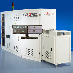
Veeco’s Propel™ Power GaN MOCVD system is designed specifically for the power electronics industry. Featuring a single-wafer reactor platform, capable of processing six- and eight-inch wafers, the system deposits high-quality GaN films for the production of highly efficient power electronic devices.

“We have been impressed with the performance of Veeco’s Propel™ GaN MOCVD platform for large-wafer 3D LED production, and naturally turned to Veeco again to support our advanced LED development,” said Philippe Gilet, co-founder and CTO of Aledia. “Veeco’s solutions meet our rigorous material quality and system delivery requirements along with unmatched material flux stability and repeatability. We are excited to take the next step with them in producing next-generation 3D micro-LEDs.”

The collaboration between Aledia and Veeco reflects the immense promise of micro-LEDs and other advanced LEDs for the future of displays. Micro-LEDs offer high efficiency, brightness and reliability benefits with shorter response time, enabling lighter, thinner and flexible displays with energy saving advantages for applications such as wearables, smartphones, automotive, signage/large TVs, augmented reality/virtual reality, etc. According to a recent Yole Développement report, there have been close to 1,500 patents filed related to micro-LED display from 125 different companies, with the bulk of activity occurring after 2012.

“With the significant shift toward exploration of micro-LEDs for use in next-generation displays, leaders like Aledia are turning to Veeco,” said Gerry Blumenstock, senior vice president and general manager of Veeco’s compound semiconductor business unit. “Veeco’s proven materials engineering expertise puts us in a unique position to offer innovative thin film deposition technologies for customers tackling tough compound semiconductor research, development and production challenges.”

Veeco will exhibit and present at the CS International Conference, March 26-27, 2019 in Brussels, Belgium. Mark McKee, director of product marketing for Veeco’s MOCVD business unit, will present “Accelerating Photonics Growth through Advances in High Performance As/P MOCVD and Wet Processing Technology,” on March 27, 2019 at 9:50 a.m. CET.

Sunday, August 20, 2017

Atomic layer etching of MOCVD epitaxial gallium nitride

As have been reported before by Lund Nano Lab in Sweden (e.g. at ALE2016 Ireland and ALE2017 Denver) it is quite possible to use a standard ICP reactive ion etch chamber to run Atomic Layer Etching (ALE). Here is a nice publication from Aalto University in Finland and current and ex scientists from Lund Nano Lab in Sweden transferring the ALE processes from Lund and running it on an Oxford Instruments Plasmalab 100 in ALE mode etching GaN in Helsinki Micronova clean room.


The Oxford Instruments Plasmalab 100 at Aalto University Micronova clean room (LINK to technical specs and capabilities) 

MOCVD grown epitaxial AlGaN/GaN heterostructures implemented in high electron mobility transistors (HEMTs) have a well-defined layered structure with the two-dimensional electron gas (2DEG). However, etching of the gate recess is challenging as conventional RIE does not provide sufficiently good control over the etch process, and high energy ions can cause damage to the 2DEG layer. This paper showcase how these problems can be avoided if GaN ALE is used in etching these recesses.


Sabbir Khan - the ALE King tuning the Plasma at Lund Nano Lab.

Besides techniques of growing a single monolayer or few monolayers of GaN are challenging. GaN ALE could provide an alternative method to the 2D material community by a controlled thinning of high quality films of GaN down to a few atomic layers.

Please find the abstract to the Open Access JVSTA publication below:


Atomic layer etching of gallium nitride (0001)
Christoffer Kauppinen, Sabbir Ahmed Khan, Jonas Sundqvist, Dmitry B. Suyatin, Sami Suihkonen, Esko I. Kauppinen, and Markku Sopanen

Journal of Vacuum Science & Technology A: Vacuum, Surfaces, and Films 35, 060603 (2017); doi: http://dx.doi.org/10.1116/1.4993996


Abstract: In this work, atomic layer etching (ALE) of thin film Ga-polar GaN(0001) is reported in detail using sequential surface modification by Cl2 adsorption and removal of the modified surface layer by low energy Ar plasma exposure in a standard reactive ion etching system. The feasibility and reproducibility of the process are demonstrated by patterning GaN(0001) films by the ALE process using photoresist as an etch mask. The demonstrated ALE is deemed to be useful for the fabrication of nanoscale structures and high electron mobility transistors and expected to be adoptable for ALE of other materials.

Thursday, February 18, 2016

Veeco Instruments, imec Enter Development Deal for Gallium Nitride Epi Wafers

Veeco Instruments reported that it has signed a joint development project (JDP) agreement with imec, a Belgium-based nano-electronics research center, to accelerate the development of Gallium Nitride (GaN) based, power electronic devices using GaN Epi wafers. Under the development project, the GaN Epi wafers will be created using Veeco’s Propel Power GaN metal organic chemical vapor deposition (MOCVD) system. Veeco’s Propel® Power GaN MOCVD system.


Veeco’s Propel™ Power GaN MOCVD system is designed specifically for the power electronics industry. Featuring a single-wafer reactor platform, capable of processing six- and eight-inch wafers, the system deposits high-quality GaN films for the production of highly efficient power electronic devices. The single-wafer reactor is based on Veeco’s leading TurboDisc® design with breakthrough technology, including the new IsoFlange™ and SymmHeat™ technologies that provide homogeneous laminar flow and uniform temperature profile across the entire wafer. Customers can easily transfer processes from Veeco K465i™ and MaxBright™ systems to the Propel Power GaN MOCVD platform. (www.veeco.com)

Imec has already demonstrated significant gains in GaN layer uniformity and run-to-run repeatability with Veeco’s Propel system, resulting in significantly improved power device yields. The single wafer reactor incorporates Veeco’s proprietary TurboDisc® technology that delivers superior film uniformity, run-to-run control and defect levels compared to batch reactors.

Friday, June 19, 2015

IKEA invests in French GaN on Silicon LED lighting technology

As reported by Electronics Weekly : Ikea’s venture capital arm has invested in a French firm developing and manufacturing 3D LEDs. Grenoble-based Aledia is developing LEDs for lighting based a gallium-nitride-on-silicon technology.


Two years after it began phasing out incandescent bulbs, Swedish retailer Ikea announced that it is taking another step and planning to sell only energy-efficient LED lighting by 2016.


Ikea believes there is this low-price LED lighting technology for residential use has the potential of faster implementation of the LED technology, leading to savings for customers.


Christian Ehrenborg, managing director of Ikea GreenTech AB, said:

“This technology will be one important part in the IKEA Group strategy to supply high-quality, energy-saving lighting products to consumers worldwide.”


Christian Ehrenborg, Bald guy.

Aledia received the investment from IKEA as part of a €28.4m funding round.

“This financing round, abundantly oversubscribed and particularly the presence of two very large potential corporate customers, testifies to the interest that our cost-disruptive nanowire LED technology is generating in the customer base, as well as in the financial community,” said Giorgio Anania, CEO, chairman and co-founder of Aledia.

Aledia is developing LEDs that are manufactured on 200mm diameter GaN-on-silicon wafers to keep cost down.

Anania said:

“We are progressing with the development of the technology and this financing round will allow us to accelerate significantly the speed of development and the customer traction. In Valeo we have a major potential customer in the automotive LED market, generally viewed as the most profitable market segment. Simultaneously with the investment, we have signed a supply agreement with Valeo.”

The technology was originally developed by CEA-Leti


Fundamental Differences in Planar and 3D LEDs

(Some background information from www.aledia.com)

Conventional LEDs are planar, two-dimensional (2D) devices that emit light from a thin material layer at or near their flat surfaces. They typically are made by depositing multiple layers of various materials, each having different thermal expansion and crystal lattice constants, on small wafers with diameters between 2 inches and 6 inches. The vast majority of LEDs are made of GaN and indium gallium nitride (InGaN) material. Depositing high-quality layers of these materials requires the GaN to be grown on substrate wafers that are made of expensive materials such as sapphire, silicon carbide or gallium nitride, as these materials are closely matched to GaN in terms of thermal expansion coefficient and crystal lattice parameters. Building planar GaN LEDs on larger and less expensive wafers made of silicon – a material that is very different from GaN in terms of thermal expansion and crystal lattice constant – is being tried, but to date this approach has shown only moderate cost savings while often incurring high defect densities, lower performance and lower yields. These factors contribute to the high costs of today’s LEDs.


In contrast, Aledia’s WireLED product technology uses economical silicon wafers with diameters of 8 inches (200 mm) or larger. On each wafer, millions of vertical microwires or microrods of GaN are grown, each with a diameter of less than 1 micron. Each microwire is an LED, capable of emitting light from all sides.


Standard Technology - 2D (Planar) LEDs:
• Small, expensive substrate
• Slow MOCVD growth process (high capital expenditure)
• High materials consumption
• LED-specific manufacturing plants
• Light emission area = at most the 2D area
• Single color on one wafer


3D (Microwire) LEDs:
• Large, economical substrate
• Fast MOCVD growth process (low capital expenditure)
• Low materials consumption
• Existing high-volume silicon wafer fabs
• Light emission area = up to 3X the 2D area = more light/mm2 or less current density, less efficiency droop
• Multiple colors on one wafer or even on one chip