Showing posts with label Dresden. Show all posts

Thursday, August 15, 2019

ALD at V2019 in Dresden October 9th to 10th with Keynote by Dr. Suntola, Millenium Technology Prize winner of 2018

We are very happy to announce the almost complete program for the ALD Workshop at V2019 in Dresden, October 9th to 10th organized by EFDS:
  • Keynote Lecture to Atomic Layer Deposition by Dr. Tuomo Suntola, Millenium Technology Prize 2018
  • Presentations to “Atomic Layer Deposition” Program (Link) 
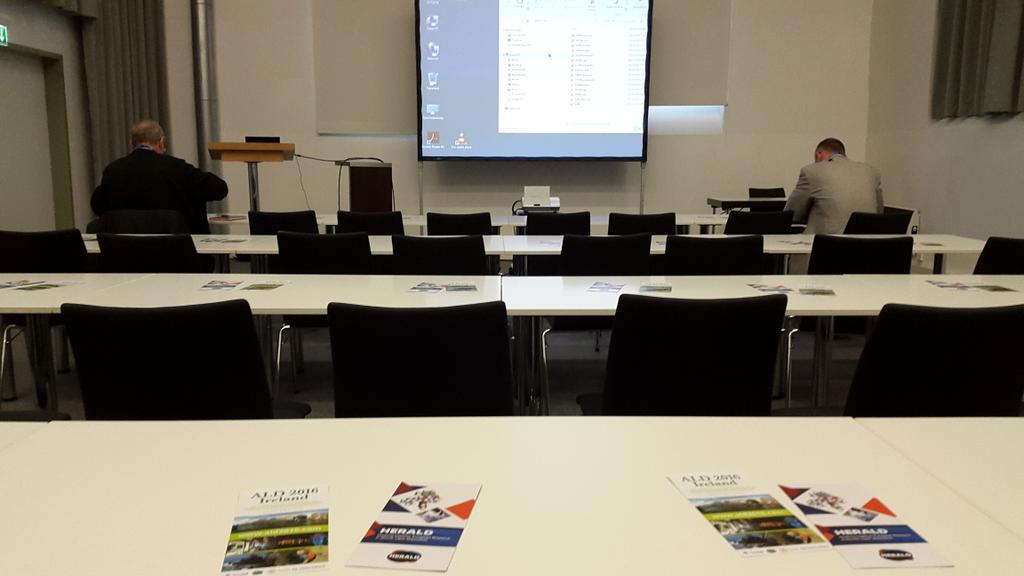
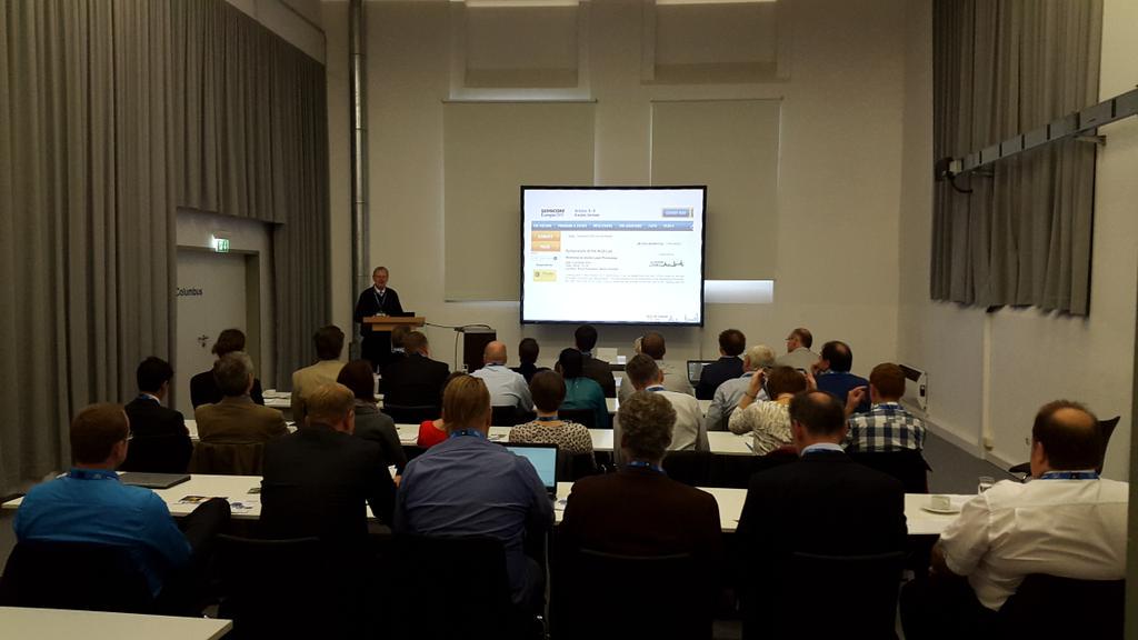
  • Workshop 5: October 9 – October 10, 2019Industrial Exhibition for Surface Technologies and adjacent Branches : Medical, Optics, Energy and ALD
  • Industrial Evening & V-Dinner
  • Information to Industrial International Funding
Downloads●  Profile of V2019 [PDF]
●  Time Schedule of V2019 [PDF]
●  Industrial Exhibition for Exhibitors [PDF]
●  Program to Atomic Layer Deposition (engl. Language) [PDF]
●  List of Exhibitors (Link)
●  Information for students and junior employees [PDF]
●  Information for job advertisements [PDF]

Lecutues | 2019.10.09 - FREE FOR ALL - No registration fee required

Lecture, part I


"45 years of ALD"
Prof. Tuomo Suntola, Picosun Oy, Espoo, Finland - Millenium Technology Prize 2018Abstract [PDF]
© Picture: By courtesy of Technology Academy Finland.
Lecture, part II
"Current and Emerging ALD Processes, Precursors and Applications in High Volume Production"
Jonas Sundqvist, Fraunhofer-Institut für Keramische Technologien und Systeme IKTS, Dresden, Germany
Abstract [PDF]
Presenations | 2019.09.10 & 2019.10.10

"Advances in quantitative characterization of thin films with help of AFM-based methods"
Malgorzata Kopycinska-Müller, Fraunhofer-Institut für Keramische Technologien und Systeme IKTS, Dresden, Germany
Abstract [PDF]

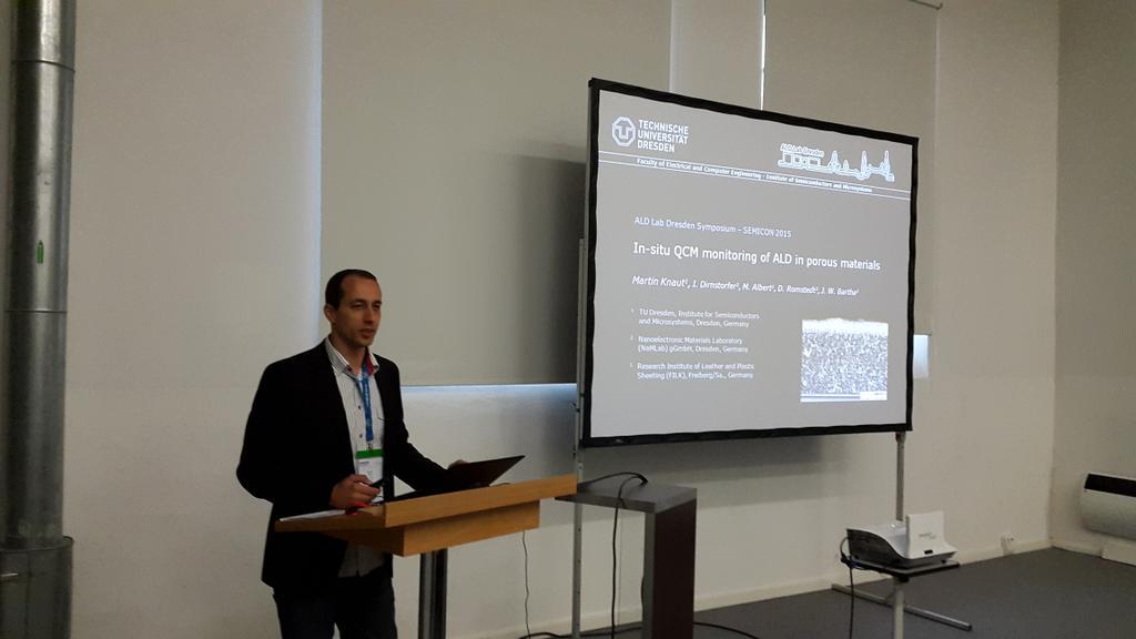
"In situ metrology for Atomic Layer Deposition processes"
Martin Knaut, Technische Universität Dresden, IHM, Dresden, Germany
Abstract [PDF]
 
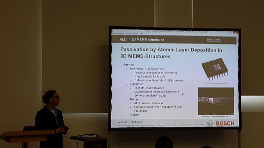
"Conformality in Atomic Layer Deposition"
Véronique Cremers, Plasma Electronic GmbH, Neuenburg, Germany
Abstract [PDF]

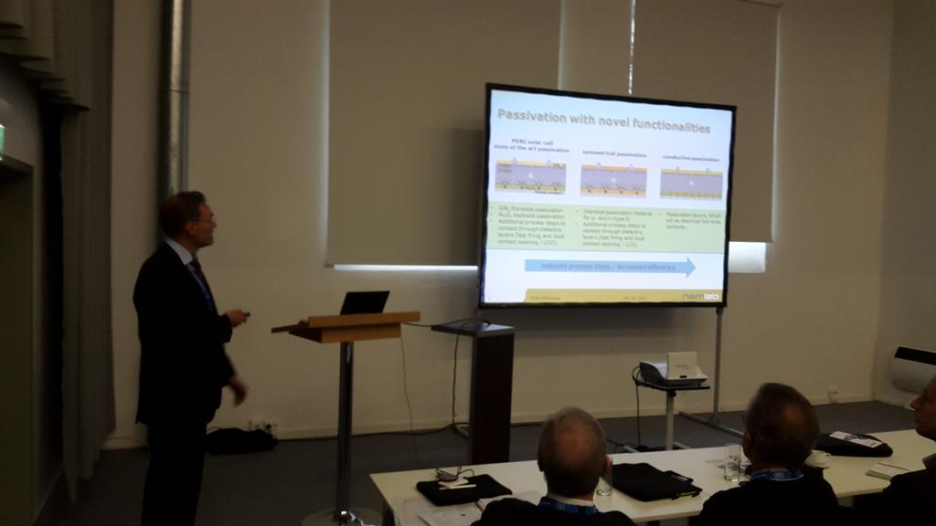
"Oxides for Electronics"
Mari Napari, Department of Materials Science and Metallurgy, University of Cambridge, Cambridge, UK
Abstract [PDF]
 
"Atomic Layer Deposition of Indium Nitride using Hexacoordinated In–N Bonded Precursors and NH3 Plasma"
Nathan O´Brian, Linköping University, Linköping, Sweden
Abstract [PDF]
 
"Multi-layer Stacked ALD Coating for Hermetic Encapsulation of Implantable Biomedical Microdevices"
Christoph Hossbach, Picosun group, Espoo, Finnland
Abstract [PDF]
 
"Fast plasma ALD employing de Laval Nozzles for high velocity precursor injection"
Abhishekkumar Thakur, Plasway-Technologies GmbH, Dresden, Germany
Abstract [PDF]

More to follow...

Friday, June 21, 2019

Aixtron partners in UltimateGaN project to make power semiconductors available for broad applications at competitive cost

[Semicondutor Today] Deposition equipment maker Aixtron SE of Herzogenrath, near Aachen, Germany says that it is a partner in the European research project UltimateGaN (research for GaN technologies, devices and applications to address the challenges of the futureGaN roadmap). In addition to Aixtron, 25 other companies and institutions from nine countries have come together to research the next generation of energy-saving chips based on gallium nitride (GaN) over the next three years. The aim is to make these power semiconductors available for a wide range of applications at globally competitive costs.


The UltimateGaN consortium consists of 26 well-established participants originating from 9 European member states and associated countries constituting a balanced mix of industry and research with complementary skills and expertise. The multidisciplinary partners cover the entire value chain technology – packaging – reliability – application.

UltimateGaN is one of the largest existing European research projects in semiconductor development. The €48m in funding consists of investment by industry, subsidies from the individual participating countries and the Electronic Components and Systems for European Leadership (ECSEL) Joint Undertaking (JU).

Efficient use of energy for climate protection


“By developing intelligent technologies, we are making a key contribution to the global challenge of climate change,” says Aixtron president Dr Felix Grawert. “New materials and efficient chip solutions play a key role here. With this research project, we are creating the conditions for making innovative energy-saving chips available for many future-oriented everyday applications,” he adds.

“Gallium nitride semiconductor devices are revolutionizing energy use on many levels,” says professor Michael Heuken, Aixtron’s VP Research & Development. “The research project opens up an enormous global market potential,” he adds. “It enables better performance and efficiency in a wide range of applications and significantly improves user comfort. Efficient operation of servers and data centers, fast and wireless charging of smartphones, data exchange between machines in real time, or lightning-fast video streaming become reality.”
Source: Semiconductor Today LINK

Saturday, March 26, 2016

ALD for Industry, 17-18 January 2017, Swissôtel Dresden Am Schloss

As you may have noticed, Dresden has developed to the German Hotbed for ALD and we want to make you aware of an ALD event in Dresden early 2017 that may be very interesting for your participation since it will have a strong Industrial focus for ALD and you will be able to reach out to the German ALD market and your potential & existing customers here.


Together with Christoph Hossbach at TU Dresden IHM I am Co-Charing this Workshop organized by EFDS (http://www.efds.org/) If you like to participate exhibit at the event please contatct.
 
contact: Grit Kotschenreuther
Gostritzer Straße 63 
kotschenreuther@efds.org
01217 Dresden Tel. +49 351 8718372


"This event provides the opportunity to learn more about fundamentals of ALD technology, to get informed about recent progress in the field and to get in contact with industrial and academic partners. Increase your visibility and present your company in our accompanying exhibition."


More information will be available soon!

Kind regards & greetings from Dresden,
Jonas & Christoph


Tuesday, January 19, 2016

A Non-FinFET Path to 10nm Globalfoundries’ FD-SOI Alternative

STMicroelectronics and CEA/Leti have been leading an effort in scaling FD-SOI for long now and have recently gotten some muscles in support by fabing it at Samsung (28nm) and Globalfoundries Fab1 in Dresden (22nm). I ran some sub 22 nm development LOTs for one of our customers some years ago and form an ALD high-k point of view this was a a piece of cake. I gave them the same recipe, adjusted the thickness slightly, as the other guys and they didn't complain. That is why I since then always follow news on FD-SOI - it´s such an underdog technology compared to bulk FinFET in terms of ecosystem support and investments but I like underdogs - or  maybe rather medium sized dogs with a big dog attitude. Anyhow here is a recent feature article by GloFo on the topic that is worth reading:

It was the coolest transistor development in many a year. Rather than continually squishing transistor parts closer and closer together, we flipped it to vertical and celebrated the arrival of the FinFET.


Image courtesy GlobalFoundries

Which was great: it gave us a way to keep increasing performance in many of the applications where the value lies in the speed of the circuit. But after the initial party was over and we started picking up the pointy party hats and nursing the hangovers with massive doses of ibuprofen, we started looking at the bill. FinFET is nice, but it’s also expensive. And, while we’re throwing stones, it’s also not so great for analog and RF designers based on the quantized nature of the gate. You can’t increase channel dimensions by 1.5 times; it’s either 1 or 2.

Rutger Wijburg announcing the investment for 22 nm FD-SOI investment at Fab1 in Dresden, Germany. (Picture by Computer-Oiger)


FinFET has been billed as the future of silicon, and Intel jumped on it, meaning everyone else had to as well. But that pounding morning-after headache is pretty strong, and there are folks wishing they had an alternative to FinFET.

Saturday, October 24, 2015

Ferroelectric HfO2 enable giant pyroelectric energy conversion and highly efficient supercapacitors

A new application for energy harvesting and storage of ferroelectric hafnium oxide has been investigated and proven by researchers at NaMLab in Dresden, RWTHA Aachen and TU Munich, Germany. One major advantage of the use of hafnium oxide over other materials is the low cost of fabrication of these films while it has been proven feasible by existing semiconductor process technology like in ALD in CMOS high-k / metal gate and high-k node dielectric for DRAM capacitors.

To summarize this investigation:
  • Ferroelectric phase transitions in Si:HfO2 thin films yield giant pyroelectricity.
  • Si:HfO2 for highly efficient supercapacitors is first reported.
  • Si:HfO2 shows highest figures of merit for pyroelectric energy harvesting.
  • Si:HfO2 for electrocaloric cooling and infrared sensing is first reported.

Ferroelectric phase transitions in nanoscale HfO2 films enable giant pyroelectric energy conversion and highly efficient super capacitors


Temperature- and field-induced phase transitions in ferroelectric nanoscale TiN/Si:HfO2/TiN capacitors with 3.8 to 5.6 mol% Si content are investigated for energy conversion and storage applications. Films with 5.6 mol% Si concentration exhibit an energy storage density of ~40 J/cm3 with a very high efficiency of ~80% over a wide temperature range useful for supercapacitors. Furthermore, giant pyroelectric coefficients of up to −1300 µC/(m2 K) are observed due to temperature dependent ferroelectric to paraelectric phase transitions. The broad transition region is related to the grain size distribution and adjustable by the Si content. This strong pyroelectricity yields electrothermal coupling factors k2 of up to 0.591 which are more than one order of magnitude higher than the best values ever reported. This enables pyroelectric energy harvesting with the highest harvestable energy density ever reported of 20.27 J/cm3 per Olsen cycle. Possible applications in infrared sensing are discussed. Inversely, through the electrocaloric effect an adiabatic temperature change of up to 9.5 K and the highest refrigerant capacity ever reported of 19.6 J/cm3 per cycle is achievable. This might enable energy efficient on-chip electrocaloric cooling devices. Additionally, low cost fabrication of these films is feasible by existing semiconductor process technology.

Wednesday, October 7, 2015

Atomic Layer Processing at SEMICON Europa 2015

Here are some ALD related pictures from SEMICON Europa in Dresden. Not only ALD since this year ALE and RIE was also a hot topic in the afternoon of the ALD Lab Dresden Symposium on Tuesday (see previous post). Biggest news here is that Oxford Instruments has released new innovative hardware for ALE!


Oxford Instruments releasing new innovative hardware for ALE (Atomic Layer Etching). Harm Knoops (right) and Andreas Stamm (left)


Assuming Oxford Instrument have big success with selling ALE hardware we will definitely start seeing an increase in ALE publications in the future and maybe the upward trend of ALD will follow or the technologies will merge into one for "Atomic Layer Processing" or like some of  us like to call it - ALX. This was actually the message from many of the presenter in the ALD Symposium (Prof. Bartha, Prof. Roozeboom, and Stephan Wege from Plasway), including this one from myself. The OEM market for ALX will definitely be very innovative and interesting in the years to come.


The Sentech stand a German OEM selling both Etch, PECVD and ALD / PEALD equipment together with very powerful in-situ ellipsometry metrology.


Nice to see that there is a lot of new activities in the European precursor supplier business. Here the team from EpiValence. EpiValence is focusing on working in collaboration with organisations looking for advanced chemicals and materials. Starting with research and development through to full scale up. You may also notice the close collaboration with iCAM (see their stand futher below)


A cross section of the popular Japanese ALD valves from KTZ SCT


Plasma Therm makes very technological advanced ICP RIE tools (Versaline) with lamp heated (!) chambers. Why these guys don´t make a PEALD chamber I don´t know - fast gas switching they do master for their Plasma wafer dicing process, which seems to be their cash cow.


Quick stop at the STREM  to talk to Jamal Belgacem about some need for new precursor and to pick up the latest catalogues for ALD precursors


I had a nice chat with Peter Barlow at iCAM - The Bubbler Maters from Wales - about building a new flexible solid evaporator for precursor screening. 


Tuesday, October 6, 2015

Photoshow : ALD Lab Dresden Symposium at SEMICON Europa 2015

SEMICON Europa this year has turned out to be a major event for ALD and exciting nanoelectronic materials research. Here are photos taken from The ALD Day October 6th, 2015!

More details on this event you can find here : http://baldengineering.blogspot.de/2015/10/ald-ale-and-exciting-nanoelectronic.html

We are already looking forward to SEMICON Europa 2016 in Grenoble, France and to co-chair an ALD Sympoium there yet one more time!

SEMICON Europa ALD 2014, Grenoble : http://baldengineering.blogspot.de/2014/10/voila-3rd-ald-lab-dresden-symposium-at.html


Columbus, Tuesday Oct 6, 13:45, ALD / ALE Sympoium of The ALD Lab Dresden, Messe Dreaden, Germany


Waiting for the ALD Storm!


Welcome
Prof. Johann W. Bartha, TU Dresden


In situ monitoring of Atomic Layer Deposition in porous materials
Martin Knaut, TU Dresden


Passivation of MEMS by Atomic Layer Deposition
Matthias Schwille, Robert Bosch


Symposium is full - please help me throw out a PVD guy


Growth Monitoring by XPS and LEIS Investigations of Ultrathin Copper Films Deposited by Atomic Layer Deposition
Dileep Dhakal, TU Chemnitz/FhG ENAS


High-k dielectrics by ALD for BEOL compatible MIM
Wenke Weinreich, FhG IPMS-CNT


ALD coatings for applications as permeation barrier and protective layer in fiber-reinforced materials
Mario Krug, FhG IKTS


ALD for solar cell application
Ingo Dirnstorfer, NaMLab


Plasma enhanced ALD process for TiO2- and WO3- films
Alexander Strobel, FH Zwickau


Why do we need Atomic Layer Etching
Jonas Sundqvist, Lund University/TU Dresden


Spatial Atomic Layer Deposition and Atomic Layer Etching
Prof. Fred Roozeboom, TU Eindhoven / TNO Eindhoven


Atomic Layer Etching: What Can We Learn from Atomic Layer Deposition?
Harm Knoops, Oxford Instruments/TU Eindhoven


Hardmask and side wall protection during dry etching with plasma enhanced deposition during dry etching for ALE purposes
Stephan Wege, Plasway


Industrial High Throughput Atomic Layer Deposition Equipment and Process for OLED Encapsulation
Jacques Kools, Encapsulix


Monolayer controlled deposition of 2D transition metal dichalcogenides on large area substrates
Annelies Delabie, Imec


Selective Deposition as Enabler for Shrinking Device Dimensions

Suvi Haukka, Executive Scientist, ASM Microchemistry Ltd.


Saturday, October 3, 2015

ALD, ALE and exciting nanoelectronic materials research at SEMICON Europa, 6-8 October, Dresden

SEMICON Europa this year has turned out to be a major event for ALD and exciting nanoelectronic materials research. Here are I have have highlighted some of the events with respect to this.


Columbus, Tuesday Oct 6, 13:45, ALD / ALE Sympoium of The ALD Lab Dresden

09:00WelcomeOrganized by:


Supported by:

cost logo


Prof. Johann W. Bartha, TU Dresden

 09:15In situ monitoring of Atomic Layer Deposition in porous materials

Martin Knaut, TU Dresden

 09:40Passivation of MEMS by Atomic Layer Deposition

Matthias Schwille, Robert Bosch

 10:05Growth Monitoring by XPS and LEIS Investigations of Ultrathin Copper Films Deposited by Atomic Layer Deposition

Dileep Dhakal, TU Chemnitz/FhG ENAS

 10:30High-k dielectrics by ALD for BEOL compatible MIM

Wenke Weinreich, FhG IPMS-CNT


 10:55ALD coatings for applications as permeation barrier and protective layer in fiber-reinforced materials
Mario Krug, FhG IKTS


 11:20ALD for solar cell application
Ingo Dirnstorfer, NaMLab


 11:45Plasma enhanced ALD process for TiO2- and WO3- films

Alexander Strobel, FH Zwickau


 12:10Lunch Break (Conversation, Networking, Finger food)


 13:00Why do we need Atomic Layer Etching

Jonas Sundqvist, Lund University/TU Dresden


 13:25Spatial Atomic Layer Deposition and Atomic Layer Etching

Prof. Fred Roozeboom, TU Eindhoven / TNO Eindhoven


 13:50Atomic Layer Etching: What Can We Learn from Atomic Layer Deposition?

Harm Knoops, Oxford Instruments/TU Eindhoven


 14:15Hardmask and side wall protection during dry etching with plasma enhanced deposition during dry etching for ALE purposes

Stephan Wege, Plasway


 14:40Industrial High Throughput Atomic Layer Deposition Equipment and Process for OLED Encapsulation

Jacques Kools, Encapsulix


 15:05Closing Remarks / Wrap Up

Prof. Johann W. Bartha, TU Dresden


 15:10End

TECH ARENA, Tuesday Oct 6, 13:45- Emerging Research, Materials and Processes Session

Potential Solutions to Semiconductor Industry’s Challenges


Chair Hessel Sprey, Manager cooperative programs and university contacts, ASM International
13:45 Introduction
13:50
Next Generation Ferroelectric Field Effect Transistors enabled by Ferroelectric Hafnium Oxide
Thomas Mikolajick, scientific director, NaMLab Gmbh / TU Dresden
14:15
Large diameter GaN-on-Si epiwafers for Power Switching and RF Power electronics with enhanced efficiency
Marianne Germain, CEO, EpiGaN nv
14:40
Prospects of Emerging 2D Transition Metal Films for Applications in Electronics
Georg Duesberg, PI, CRANN, Trinity College Dublin
15:05
Monolayer controlled deposition of 2D transition metal dichalcogenides on large area substrates
Annelies Delabie, Professor, Imec
15:30
Selective Deposition as Enabler for Shrinking Device Dimensions
Suvi Haukka, Executive Scientist, ASM Microchemistry Ltd.
15:55
MOFs as Low-k Candidates for Future Technology Nodes
Christof Wöll, Director, KIT
16:20
Spin-based nanoelectronic devices for mobile Informaion-Communication Technology
Alina Deac, Group Leader, Helmholtz-Zentrum Dresden - Rossendorf
16:55 Closing Remarks

ARENA 2: Tuesday, 6 October 2015, Best of Advanced Process Control (APC)

12:25   In-Situ process control for Atomic Layer Deposition (ALD)
Johann W. Bartha, TU Dresden

Wednesday, September 30, 2015

The agenda for the ALD Lab Dresden Symposium at SEMICON Europa is now set!

The agenda for the ALD Lab Dresden Symposium is now set! If you are attending and representing a company or any organization with an offering in ALD or ALE - please brig alog your flyers, coffee mugs, hats and pensand I will sort out a table that is bug enought for displaying it.


AGENDA


 Tuesday, 6 October 2015

 09:00WelcomeOrganized by:


Supported by:

cost logo


Prof. Johann W. Bartha, TU Dresden

 09:15In situ monitoring of Atomic Layer Deposition in porous materials

Martin Knaut, TU Dresden

 09:40Passivation of MEMS by Atomic Layer Deposition

Matthias Schwille, Robert Bosch

 10:05Growth Monitoring by XPS and LEIS Investigations of Ultrathin Copper Films Deposited by Atomic Layer Deposition

Dileep Dhakal, TU Chemnitz/FhG ENAS

 10:30High-k dielectrics by ALD for BEOL compatible MIM

Wenke Weinreich, FhG IPMS-CNT


 10:55ALD coatings for applications as permeation barrier and protective layer in fiber-reinforced materials
Mario Krug, FhG IKTS


 11:20ALD for solar cell application
Ingo Dirnstorfer, NaMLab


 11:45Plasma enhanced ALD process for TiO2- and WO3- films

Alexander Strobel, FH Zwickau


 12:10Lunch Break (Conversation, Networking, Finger food)


 13:00Why do we need Atomic Layer Etching

Jonas Sundqvist, Lund University/TU Dresden


 13:25Spatial Atomic Layer Deposition and Atomic Layer Etching

Prof. Fred Roozeboom, TU Eindhoven/ TNO Eindhoven


 13:50Atomic Layer Etching: What Can We Learn from Atomic Layer Deposition?

Harm Knoops, Oxford Instruments/TU Eindhoven


 14:15Hardmask and side wall protection during dry etching with plasma enhanced deposition during dry etching for ALE purposes

Stephan Wege, Plasway


 14:40Industrial High Throughput Atomic Layer Deposition Equipment and Process for OLED Encapsulation

Jacques Kools, Encapsulix


 15:05Closing Remarks / Wrap Up

Prof. Johann W. Bartha, TU Dresden


 15:10End

Friday, September 18, 2015

UPDATE: Symposium of The ALD Lab Dresden at SEMICON Europa

Symposium of the ALD-Lab

Workshop on Atomic Layer Processing

Date: 6 October 2015
Time: 09:00 - 15:10
Location: Room Columbus, Messe Dresden


Looking back in the evolution of IC technology, it can be stated that from the 0.25µm node on, the key for further shrinking was planarization. This was enabled by the introduction of an emerging technology, the CMP. Since the 28 nm node it can be observed that, at least in the front end of line, starting with the FinFET and possibly continuing with the surrounding gate transistor, the required structures become more and more three dimensional, while the thickness of the associated films become extremely thin (gate dielectric, work function layer, barrier layer). The emerging technology enabling this is Atomic Layer Deposition (ALD).
ALD is based on self limiting heterogeneous chemical reactions which allow the fabrication of very thin (sub nm to few nm) layers with high accuracy (basically atomic layer precision), extremely well conformality and intrinsically high uniformity even in batch tools. Although the scientific background of ALD goes far back in history, ALD for semiconductor processing can still be considered as a novel technology.
Progress in ALD is associated with tools, but even more with specifically designed precursors which need to be applied at optimum conditions of the gas feed system, the process chamber and the substrate condition. Our workshop, which is organized by the “ALD Lab Dresden” wants to stimulate discussions between developers of tools, consumables, as well as applicants of this exciting technology.
The self limiting behavior of the heterogeneous reaction can however also be used to remove material from a substrate in an extremely controlled fashion of atomic dimensions. This process, that can be viewed as the complement to ALD is called Atomic Layer Etching (ALEt). As for ALD also ALEt can be a game changer for the semiconductor industry utilizing surface functionalization and modification similar to those we know in ALD and resulting in a chemistry-based material removal on the same atomic level as in ALD – A layer by layer removal.
In general scaling is thought about to be a shrink in the critical dimensions (CD, pitch) in the latheral xy-plane, today scaling is also taking place in the z-direction, i.e.,  a reduction in the thickness of the film stacks like the High-k Metal Gate stack. This has resulted in that the thicknesses of the film stacks of devices today are now routinely approaching <20 Å nm providing an opportunity for slow and precise etching by ALEt.
We hope that this new part of the ALD Lab Dresden Symposium will allow for increased scientific and technological discussion for enabling ALEt and learning from ALD and related plasma based processing techniques like Plasma CVD and Reactive Ion Etching.


AGENDA


 Tuesday, 6 October 2015

 09:00WelcomeOrganized by:


Prof. Johann W. Bartha, TU Dresden

 09:15In situ monitoring of Atomic Layer Deposition in porous materials

Martin Knaut, TU Dresden

 09:40Passivation of MEMS by Atomic Layer Deposition

Matthias Schwille, Robert Bosch

 10:05Growth Monitoring by XPS and LEIS Investigations of Ultrathin Copper Films Deposited by Atomic Layer Deposition

Dileep Dhakal, TU Chemnitz/FhG ENAS

 10:30High-k dielectrics by ALD for BEOL compatible MIM

Wenke Weinreich, FhG IPMS-CNT


 10:55ALD coatings for applications as permeation barrier and protective layer in fiber-reinforced materials
Mario Krug, FhG IKTS


 11:20ALD for solar cell application
Ingo Dirnstorfer, NaMLab


 11:45Plasma enhanced ALD process for TiO2- and WO3- films

Alexander Strobel, FH Zwickau


 12:10Lunch Break (Conversation, Networking, Finger food)


 13:00Why do we need Atomic Layer Etching

Jonas Sundqvist, Lund University/TU Dresden


 13:25Spatial Atomic Layer Deposition and Atomic Layer Etching

Prof. Fred Roozeboom, / TNO Eindhoven


 13:50Atomic Layer Etching: What Can We Learn from Atomic Layer Deposition?

Harm Knoops, Oxford Instruments/TU Eindhoven


 14:15Hardmask and side wall protection during dry etching with plasma enhanced deposition during dry etching for ALE purposes

Stephan Wege, Plasway


 14:40Industrial High Throughput Atomic Layer Deposition Equipment and Process for OLED Encapsulation

Jacques Kools, Encapsulix


 15:05Closing Remarks / Wrap Up

Prof. Johann W. Bartha, TU Dresden


 15:10End


Registration

No pre-registration required but you must register as a visitor, in order to gain access to the venue: