Showing posts with label Dresden. Show all posts

Monday, August 24, 2015

ALD Lab Dresden sends away Varun Sharma to Helsinki, Finland


ALD Lab Dresden, Institut für Halbleiter- ind Mikrosystemtechnik at TU Dresden takes farewell and sends away Varun Sharma to Helsinki, Finland to learn from the masters how to ALD. Please take good care of Varun for us because he too was born to ALD. (Varun Sharma, Christoph Hossbach, Jonas Sundqvist, Martin Knaut)


Thursday, August 6, 2015

Heliatek solar films awarded with World Economic Forum's Technology Pioneers

Heliatek, the Dresden-based German company that produces ultra-light, flexible and less than 1 mm thick Photovoltaic solar films, was awarded today as one of the World Economic Forum's "technology pioneers", a selection of the world's most innovative companies. Heliatek is a spin-off from the Technical University of Dresden and the University of Ulm. The company is a leader in the field of Organic Electronics Energy holding the world record efficiency of 12%. It started commercialization of its solar films in July 2014. 


The tandem cell: two solar cells stacked on top of each other. The active layers are only around 250 nm thick. (www.heliatek.com)
 
Heliatek was chosen by a professional jury from among hundreds of candidates as one of the 49 selected companies and was the only German company to do so. Thanks to its selection, it will have access to the most influential and sought-after business and political network in the world, and be invited to the World Economic Forum's "Summer Davos" in Dalian, China, this September, or the Annual Meeting in Davos in January.


Thibaud Le Séguillon, Heliatek CEO, remarks, "We are delighted to be recognized by The World Economic Forum as a Technology Pioneer. We have developed groundbreaking technology and manufacturing process that will have a significant impact on the way energy is produced. By integrating our solar films to building facades, we turn these into localized power stations."

 
Heliatek  hold the world record of 12% cell efficiency for opaque (non-transparent) organic solar cells. In production, they currently achieve 7-8 %. The latest development allows transparency levels up to 50% with an efficiency of 6%. The intrinsic lifespan of our small molecules is >25 years (extrapolated). (www.heliatek.com)


"We're glad to see a German company make it to the selection," says Fulvia Montresor, Head of Technology Pioneers at the World Economic Forum. "Heliatek is part of a group of entrepreneurs who are more aware of the crucial challenges of the world around them, and who are determined to do their part to solve those challenges with their company."
 

The innovative roll-to-roll production process offers many advantages: high throughput, high yield and low costs. For example only 1g of organic material is necessary for one square meter (1m²= 10.74 ft²) of active HeliaFilm®. Together with the low power consumption of the production process this leads to a uniquely short energy payback time of less than 3 months. (www.Heliatek.com)
 
The Technology Pioneers were selected from among hundreds of applicants by a selection committee of 68 academics, entrepreneurs, venture capitalists and corporate executives. Notable members of the committee include Arianna Huffington (founder, Huffington Post) and Henry Blodget (editor-in-chief, Business Insider). The committee based its decisions on criteria including innovation, potential impact, working prototype, viability and leadership.

Past recipients include Google (2001), Wikimedia (2007), Mozilla (2007), Kickstarter (2011) and Dropbox (2011). More information on past winners can be found here.

Wednesday, July 29, 2015

Helmholtz to invest 46 million EUR in a Energy Materials Foundry (HEMF)

Six Helmholtz Centres are founding a shared infrastructure for developing novel energy materials that will also be available to external users. The Helmholtz Senate has approved setting up a major infrastructure to synthesise and develop novel systems of materials for energy conversion and storage. Total funding will be 46 million EUR (2016-2020).


The Helmholtz Association performs cutting-edge research which contributes substantially to solving the grand challenges of science, society and industry. Scientists at Helmholtz concentrate on researching the highly-complex systems which determine human life and the environment. For example, ensuring that society remains mobile and has a reliable energy supply that future generations find an intact environment or that treatments are found for previously incurable diseases. The activities of the Helmholtz Association focus on securing the foundations of human life long-term and on creating the technological basis for a competitive economy. The potential with which the Association achieves these goals is made up of the outstanding scientists working at the research centres, a high-performance infrastructure and modern research management.

The Helmholtz Energy Materials Foundry (HEMF) will be coordinated by the Helmholtz-Zentrum Berlin, while five additional Helmholtz Centres are participating in the design, planning, and setup: the German Aerospace Center (DLR), Forschungszentrum Jülich (FZJ), Helmholtz-Zentrum Geeshacht (HZG) for Materials and Coastal Research, Helmholtz-Zentrum Dresden-Rossendorf (HZDR), and the Karlsruhe Institute of Technology (KIT). The HEMF platform will also be open to external users from universities and non-university institutes from Germany and abroad, as well as to industry.

Several outstanding supplementary laboratories with unique equipment will be set up under HEMF at the six participating Helmholtz Centres. The scientific focus lays on the design of energy materials associated with solar fuels, solar cells, and battery systems as well as thermoelectric and thermochemical materials. One research topic these applications share is the design of novel catalysts to be employed in energy conversion and storage.


Hermann Ludwig Ferdinand Helmholtz born in Potsdam 1821 studied at the Berlin Military Academy and gained his Doctor of Medicine in 1842.  He took the chair of physiology and pathology in Königsberg on the recommendation of Alexander von Humboldt, which he held until 1855. Other chairs followed, in Bonn (1855 to 1858) and Heidelberg (1858 to 1871). From 1871, Helmholtz became professor of physics and taught at the University of Berlin. In the late 1880s, he became the founding president of the Physikalisch-Technische Reichsanstalt in Charlottenburg, which he himself and Werner von Siemens had established and which continues even today - as the Physikalisch Technische Bundesanstalt (PTB) - to serve the science of metrology.

The range of capabilities of the HEMF platform extends from the design of novel materials systems, to in-situ and in-operando analyses of processes for their synthesis, and three-dimensional nanostructuring of these materials to alter their properties in specific ways. In addition, new methods will be developed to process novel materials, produce innovative prototypes for specific applications, and investigate their properties and capabilities under continuous loads. “This comprehensive approach enables creation of efficient feedback loops between synthesis, characterisation, and the evaluation of the end products. It will help us accelerate knowledge-based development”, says Prof. Anke Kaysser-Pyzalla, Scientific Director of HZB.


HZB’s BESSY II facility in Berlin

Synthesis laboratories are planned at HZB specifically for perovskite thin films, nanoparticles for catalysis and electrochemical storage, as well as facilities for nanostructuralisation of materials. New methods will be developed for studying electrochemical processes at catalytic and heterogenous boundary surfaces by the Energy Materials in-situ Laboratory (EMIL) recently set up at HZB’s BESSY II facility. Moreover, testing labs are also being set up in order to study new systems of materials under actual operating conditions. HZB is working together on this with the Max Planck Society’s Fritz Haber Institute in Berlin and the Max Planck Institute for Chemical Energy Conversion (CEC) in Mülheim.

The HEMF platform will be operated as an international user facility. The laboratories will be available to research teams from universities, non-university research institutions, and industry. The coordination of user operations will be handled by HZB, which has a great deal of experience with this and has built up outstanding user services for its own large-scale facilities BESSY II and BER II. About 3000 external personnel visiting for purposes of conducting measurements benefit from these services annually. HEMF builds on the model of Berkeley Labs in California, where a Molecular Foundry was also set up as an infrastructure serving international user groups.


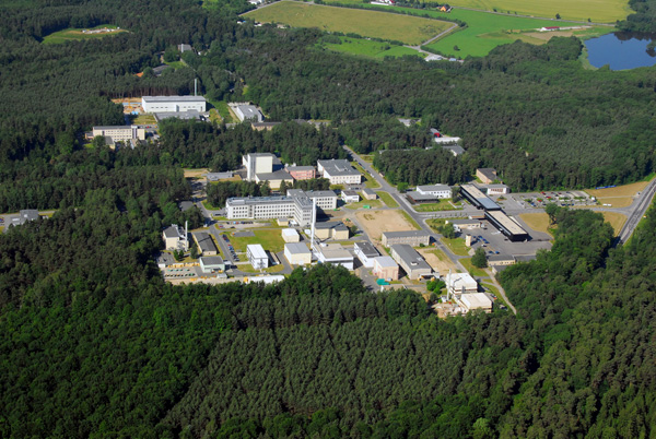
HZDR in Rossendorf in the forest west of Dresden

“HEMF will augment the Helmholtz Association’s expertise in synthesis of raw materials indispensable for the energy transition. The participating Helmholtz Centres will be able to add their research capabilities to this shared infrastructure so that we can make the energy we will need in the future available for use in a safe and simultaneously environmentally friendly way. At the same time, the platform will draw attractive collaborating partners who are pursuing the same research goals”, Kaysser-Pyzalla explains further. This research plan’s unique order of magnitude will help the group of Helmholtz Centres contribute R&D on new energy materials – a contribution that will be comparably large and pioneering on an international scale as well.


A cluster vacuum tool at the ion beam center at HZDR.

According to this report by Heiko Weckbrodt (Computer Oiger) Helmholtz-Zentrum Dresden-Rossendorf (HZDR) will invest 3,5 M Euro in the existing Ion beam center and a new lab for nano lithography and analytics.

Tuesday, July 14, 2015

Germany to fund the Semiconductor industry with 400 milion Euro

"Every second chip made in Europe comes from Saxony!"

Happy days in Dresden, Silicon Saxony and Germany today - Yesterday Globalfoundries announced that they are investing in Fab 1 in Dresden to ramp 22 nm FD-SOI and today Angela Merkel and Johanna Wanka comes for a visit to Dresden and promises 400 million Euro support package until 2020 for the semiconductor industry!


"Um Innovationen in der Halbleiterindustrie auch künftig voranzutreiben, erarbeitet das Bundesforschungsministerium bis Ende des Jahres zusammen mit weiteren Ressorts ein neues Rahmenprogramm. Das Programm soll mit einem Volumen von 400 Millionen Euro bis 2020 ausgestattet werden. Das hat Bundesforschungsministerin Wanka bei ihrem Besuch in Dresden angekündigt. " - http://www.bmbf.de/de/28961.php

Chancellor Angela Merkel entering the helicopter in Berlin to fly 200 km south to Dresden. (Twitter, BMBF)


Rutger Wijburg (VP and General Manager Fab1, Dresden) explains factory physics for Sanjay Jha (CEO Globalfoundries) Chancellor Angela Merkel, Ministerpräsident Stanislaw Tillich and Bundesforschungsministerin Johanna Wanka using a model Globalfoundries Fab 1 in Dresden. (Photo: Heiko Weckbrodt)

More details for those of you reading German can be found in the excellent coverage by Heiko Weckbrodt :

Bund sagt 400 Millionen € für Mikroelektronik zu

Kanzlerin Merkel debattiert in Dresden Mikroelektronik-Strategie

MDR Sachsen Video in German:

Overview
http://www.mdr.de/sachsenspiegel/video284012.html

Silicon Saxony
http://www.mdr.de/sachsenspiegel/video284020.html

Globalfoundries
http://www.mdr.de/sachsenspiegel/video283788.html


Later Frau Bundeskanzlerin Dr Merkel also stopped by Fraunhofer to meet with The Fraunhofer President Prof. Dr. Reimund Neugebauer.


Angela Merkel also visited Infineon’s Dresden 300 and 200 mm fabs today and discussed the political framework for a competitive development and production in Germany with CEO Reinhard Ploss. - See more at: http://www.electronicsweekly.com/news/business/merkel-visits-infineon-dresden-fab-2015-07/#sthash.XHTLv12Y.dpuf


Yesterday, flanked by two clean room engineers posing with 300 mm device wafers the Globalfoundries Managers Gregg Bartlett, Sanjay Jha (CEO) und Rutger Wijburg (VP and General Manager Fab1, Dresden) announce that Globalfoundries will invest $250 million for 22nm FD-SOI production in Fab 1 Dresden, Germany. From the press conference in Dresden (photo by Heiko Weckbrodt, www.computer-oiger.de)

Monday, July 13, 2015

GLOBALFOUNDRIES Launches Industry’s First 22nm FD-SOI Technology Platform in Dresden

GLOBALFOUNDRIES today launched a new semiconductor technology developed specifically to meet the ultra-low-power requirements of the next generation of connected devices. The “22FDX™” platform delivers FinFET-like performance and energy-efficiency at a cost comparable to 28nm planar technologies, providing an optimal solution for the rapidly evolving mainstream mobile, Internet-of-Things (IoT), RF connectivity and networking markets.

Flanked by two clean room engineers posing with 300 mm device wafers the Globalfoundries Managers Gregg Bartlett, Sanjay Jha (CEO) und Rutger Wijburg today announced at a press event that Globalfoundries will invest $250 million for 22nm FD-SOI production in Fab 1 Dresden, Germany.


Flanked by two clean room engineers posing with 300 mm device wafers the Globalfoundries Managers Gregg Bartlett, Sanjay Jha (CEO) und Rutger Wijburg (VP and General Manager Fab1, Dresden) announce that Globalfoundries will invest $250 million for 22nm FD-SOI production in Fab 1 Dresden, Germany. From the press conference in Dresden (photo by Heiko Weckbrodt, www.computer-oiger.de)

While some applications require the ultimate performance of three-dimensional FinFET transistors, most wireless devices need a better balance of performance, power consumption and cost. 22FDX provides the best path for cost-sensitive applications by leveraging the industry’s first 22nm two-dimensional, fully-depleted silicon-on-insulator (FD-SOI) technology. It offers industry’s lowest operating voltage at 0.4 volt, enabling ultra-low dynamic power consumption, less thermal impact, and smaller end-product form-factors. The 22FDX platform delivers a 20 percent smaller die size and 10 percent fewer masks than 28nm, as well as nearly 50 percent fewer immersion lithography layers than foundry FinFET.

“The 22FDX platform enables our customers to deliver differentiated products with the best balance of power, performance and cost,” said Sanjay Jha, chief executive officer of GLOBALFOUNDRIES. “In an industry first, 22FDX provides real-time system software control of transistor characteristics: the system designer can dynamically balance power, performance, and leakage. Additionally, for RF and analog integration, the platform delivers best scaling combined with highest energy efficiency.”

"The 22nm process overcomes some challenges at 28nm. The transistor is better and the 20 percent area scaling we get makes up for the cost of the substrate," Jha said. "That means we can offer better performance at the same cost as 28nm [alternatives to FD-SOI]," Jha added in EE Times Europe.


The Dresden Fab 1 with a capacity: 60,000 wafers/month (300 mm)Technology: 45nm to 28nm and now also 22 nm (www.globalfoundries.com)

22FDX leverages the high-volume 28nm platform in GLOBALFOUNDRIES’ state-of-the-art 300mm production line in Dresden, Germany. This technology heralds a new chapter in the “Silicon Saxony” story, building on almost 20 years of sustained investment in Europe’s largest semiconductor fab. GLOBALFOUNDRIES launches its FDX platform in Dresden by investing $250 million for technology development and initial 22FDX capacity. This brings the company’s total investment in Fab 1 to more than $5 billion since 2009. The company plans to make further investments to support additional customer demand. GLOBALFOUNDRIES is partnering with R&D and industry leaders to grow a robust ecosystem and to enable faster time-to-market as well as a comprehensive roadmap for its 22FDX offering. 

Full story here: http://globalfoundries.com/newsroom/press-releases/2015/07/13/globalfoundries-launches-industry-s-first-22nm-fd-soi-technology-platform


Furthermore, Rutger Wijburg, senior vice president and general manager of the Dresden Fab 1, acknowledged that Globalfoundries is taking part in European Commission administered projects such as Horizon 2020. "We plan to extend that activity," Wijburg said according to EE Times Europe. As far as I know one of them is WAY-TO-GO CMOS headed by ST Microelectronics