Showing posts with label materials. Show all posts

Thursday, July 13, 2023

2023 Semiconductor Materials Market Slowing but Resilient

Material growth to resume in 2024 as industry recovers and fabs ramp up

San Diego, CA, July 12, 2023: TECHCET—the electronic materials advisory firm providing business and technology information— announced that the Total Semiconductor Materials market will contract by at least -3% in 2023 given the industry wide slowdown and reported higher levels of inventory in the materials supply chain. This year’s decline will result in revenues for Semiconductor Materials to total US$69.6 billion, down from the US$71.7 reported in 2022. However, leading-edge logic and automotive/power device production will limit the overall decline in materials revenues for 2023.
TECHCET is forecasting a strong recovery in the market in 2024, with total material revenues increasing 8% to almost US$75 billion. CAGR growth over the next 5 years is forecasted to be 4%, which will result in the market reaching US$88 billion by 2027.


To read the full article, go to: https://lnkd.in/gVan5qSq

To find out more: see TECHCET at SEMICON West at NY CREATES Booth (North Hall 5845) from July 11-13. Lita Shon-Roy, Diane Scott, Dan Tracy, and Kevin McLaughlin will all be there to share market insights and industry updates. Or visit our website here: https://lnkd.in/gJQ2Gt36.

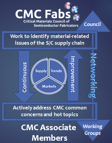
Segment summarized by TECHCET previous recent releases:

Semiconductor Metal Plating Chemicals:

The market for semiconductor metal plating chemicals is expected to experience a slight decrease of 2% in 2023. This decline is due to lower expectations for overall wafer starts and inventory corrections within the market. Copper is the largest revenue contributor in this segment, particularly in advanced packaging wiring and interconnect copper plating. However, the market is expected to rebound in the long term, with a positive compound annual growth rate (CAGR) of 3.7% for advanced packaging and 3.3% for interconnect metal chemicals.

Semiconductor Quartz Equipment Components:

After reaching an all-time high in 2022, the market for fabricated quartz equipment components is expected to decline in 2023. The slowdown is attributed to a shift in industry investments and reduced purchase orders. However, the market is buoyed by previous purchases and backlogs, leading to a projected decline of 6% in 2023. New fab expansions are expected to drive future growth, with a CAGR of 5% from 2022 to 2027.

CMP Consumables:

Following strong performance in 2022, the CMP consumables market is forecasted to experience a slight reduction of 2.4% in 2023. The decrease is primarily due to oversupply in DRAM and market corrections. However, the market is expected to achieve a 5-year CAGR of 5.2%. The demand for new metals pads and slurry is anticipated to drive growth in this segment, particularly with the development of advanced logic methodologies and the evaluation of new BEOL materials.

Electronic Gases:

The electronic gases market is expected to witness a positive 5-year CAGR of 6.4% driven by expansions within the semiconductor industry, especially in leading-edge logic and 3DNAND applications. However, supply constraints for critical gases like B2H6 and WF6 may arise as demand outpaces supply. Disruptions in gas supply from current sources and geopolitical events may lead to shortages. Helium supply is also considered at high risk. Despite these challenges, the market is projected to grow, particularly with new fab expansions and increasing demand.

Semiconductor Wet Chemicals:

Semiconductor wet chemical revenues are forecasted to decline by 2% in 2023, following the trends in wafer starts and rising energy prices. The industry slowdown and instability from the Russia-Ukraine war contribute to the market contraction. However, the market is expected to rebound in 2024, with a 5-year CAGR of 3.9%. Phosphoric acid is the strongest segment within wet chemicals due to growth in the 3DNAND market. A holistic approach to the chemical supply chain is crucial for success in this market.

ALD/CVD Precursors:

The market for ALD/CVD precursors experienced a flattening in 2023 due to reduced memory pricing in production. However, a rebound is expected in the second half of the year, driven by the recovery of memory pricing. The market for high-ƙ and low-ƙ dielectric precursors is projected to rebound significantly in 2027, with a growth rate of approximately 19%. The market will be boosted by fab expansions, logic advancements, and increasing demand for metal and dielectric precursors.

Tuesday, January 12, 2021

Semiconductor Materials $50B Market on a Strong Run in 2021

Semiconductor Materials $50B Market on a Strong Run in 2021Pandemic pushing people to Work From Home and School From Home

San Diego, CA, January 12, 2021: TECHCET announced that global revenues for semiconductor manufacturing and packaging materials grew approximately 4% year-over-year (YoY) in 2020 to ~US$50B, and are expected to grow ~7% in 2021 to nearly US$54B. The COVID-19 pandemic has created strong demand for both logic and memory ICs to support Work From Home (WFH) and School From Home (SFH), and such demand is expected to increase despite expanding availability of virus vaccines. Also, demand for automotive ICs has recovered and will be an important driver in 2021 growth. The compound annual growth rate (CAGR) through 2024 is forecast at 5.3% as per the latest TECHCET Critical Materials Reports (CMR) and shown in the attached figure.

Analysts' Alerts emailed to CMR purchasers help them anticipate and mitigate potential supply-chain disruptions. Excerpts have been publicly disclosed on the following critical materials (https://lnkd.in/dzAZcCw):

* IPA in "CMC Considers Bio-Solvents to Reduce Fab Risks",
* HF in "Semi Wet Chemicals US$2B Market Threatened by Localization", and
* Lanthanum in "Rare Earth Elements (REE) Supply Uncertain for IC Fabs".


Tuesday, April 28, 2020

CMC Workshop Flags Looming Shortages of IPA and Sulfuric Critical Materials

Council (CMC) of semiconductor fabricators & suppliers is now meeting several times a month to mitigate potential supply-chain disruptions. The last meetings exposed likely shortages in iso-propyl alcohol (IPA) and sulfuric acid looming just over the business horizon due to the COVID-19 pandemic. The CMC has now opened attendance at monthly COVID-19 Briefings and Virtual Workshops to pre-registrants for the 2020 CMC Conference, happening October 22-23 in Hillsboro, Oregon. 
Fabs and suppliers say that the supply-chain for semiconductor-grade IPA has capacity to meet current global requirements (Figure). 
However, due to COVID-19, some of the industrial IPA supply-chain is re-directed to healthcare and consumer distribution, increasing overall demand. Spot prices for this critical material have reportedly increased a staggering 30% month-over-month (MoM). IPA depends on propene feedstock from oil refiners, and the current economic slowdown has reduced oil demand to such an extent that refineries are being idled. TECHCET has put up "cautionary flags" to watch for 2H20 shortages of IPA and sulfuric acid, as per the latest quarterly update to TECHCET's Wet Chemicals & Specialty Cleans analysis.

ABOUT TECHCET: TECHCET CA LLC is an advisory service firm focused on process materials supply-chains, electronic materials technology, and materials market analysis for the semiconductor, display, solar/PV, and LED industries. Since 2000, the company has been responsible for producing the Critical Material Reports™ for the Critical Materials Council (CMC), covering silicon wafers, semiconductor gases, wet chemicals, CMP consumables, Photoresists, and ALD/CVD Precursors. For additional information about these reports or CMC subscription membership please contact info@techcet.com, +1-480-332-8336, or go to www.techcet.com

Monday, April 20, 2020

Choppy Waters for Shipping $50B of Semiconductor Materials in 2020

Risky Sailing on the Global Supply-Chain Seas

San Diego, CA, Apr 17, 2020:TECHCET announces that:
 
• 2020 global material revenues in semiconductor manufacturing forecasted to decline by 3.0% year-over-year (YoY) despite growth in 1Q2020,
• Impact of COVID-19 pandemic on the global economy is creating choppy waters for shipping and supplying critical materials, as highlighted in recent Critical Materials Council (CMC) monthly meetings, and
• With a return of global economic growth by 2021, compound annual growth rate (CAGR) through 2025 is forecast at 3.5% as shown in the Figure (below).


“From our market research, materials suppliers are increasing production and sales to ensure safety-stock throughout the supply-chain in case there are further disruptions due to COVID-19 cases,” remarked Lita Shon-Roy, TECHCET President and CEO. “Even without further disruptions, we can already see leading economic indicators such as unemployment levels, metal prices and container shipping indices point toward a significant decline in global GDP.” This is supported by the International Monetary Fund’s (IMF’s) current outlook on 2020.

Currently, almost all chip fabs appear to be running at normal levels, with a few exceptions. During this difficult period, YMTC in Wuhan, China reportedly has maintained R&D and grown production of 3D-NAND chips. However, chip fabs in Malaysia report that the government required companies to request permission to continue operating at 50% staffing levels. One company in France had to temporarily reduce production due to their labor union insisting on temporary workforce reductions.

Significant value-added engineered materials including specialty gases, deposition precursors, wet chemicals, chemical-mechanical planarization (CMP) slurries & pads, silicon wafers, PVD/sputtering targets, and photoresists & ancillary materials for lithography are reporting healthy orders and in some cases will see better than expected revenues for 1Q2020 and April 2020. However, more than 60% of all materials are expected to be negatively impacted before year-end.

Overall demand for commodity materials, such as silane and phosphoric acid, is expected to decline YoY in 2020 by an average of 3% due to softening of the global economy. Average selling prices (ASP) for electronic-grade commodities may drop due to cost reductions in feed-stocks; for example, the global helium (He) gas market which had been forecasted to be in shortage with high ASPs throughout 2020 has already improved due to COVID-19 slowing down helium demand.

DRAM, 3D-NAND, and MPU chips for server / cloud-computing applications are now in high demand for virtual meetings and remote work. It is yet unclear how much of an increase in materials shipments will be needed to support this segment, however from TECHCET’s modeling of prior cycles it will likely be >7%. Despite such an increase in the materials used to make leading-edge ICs to build out data centers, shipments in support of legacy node IC fabrication are expected to decline this year.

Consequently, cloud-computing growth may not compensate for overall reduced semiconductor materials demands caused by economic downturns this year. By 2021 the global economy and all chip fabs should return to healthier growth, with materials markets for all IC devices expected to increase at a CAGR of +3.5% through 2025.

Critical Materials Reports™ and Market Briefings: TECHCET Shop
CMC Events: Click here to view all Events

Thursday, January 10, 2019

Semiconductor Materials Market will be +3% to $50.4B in 2019

TECHCET-the electronic materials advisory services firm providing business and technology information- announced that global revenues for semiconductor manufacturing and packaging materials are expected to grow 3.1% year-over-year (YoY) in 2019 to US$50.4B, of which 58% represents semiconductor fab materials. Steadily increasing demand for memory chips in 2018 lifted total materials market revenues to US$48.9B in 2018, while the compound annual growth rate (CAGR) through 2023 is forecast at 4.3% as detailed in the latest TECHCET Critical Materials Reports (CMR) and shown in the attached figure.


Global trade issues in 2018 run the risk of devolving into real trade wars, if governments and companies do not negotiate business terms from a place a mutual respect. "Wars can only have winners and losers," reminded Lita Shon-Roy, TECHCET President and CEO. "While issues can have win-win resolutions after mutually-respectful negotiations." 


At the 2018 Critical Materials Council (CMC) Seminar, held last October in Ningbo, China in coordination with China's IC Materials Technology Innovation Alliance (ICMtia), representatives of global chip-makers including Intel, GlobalFoundries, and Texas Instruments discussed ways to ensure electronic materials supply-chain robustness in an era of short-sighted protectionist tariffs. All three companies have high-volume manufacturing (HVM) fabs in mainland China along with the US, and all need to source a wide range of specialty materials from global suppliers.

During private face-to-face meetings between CMC fab members in Ningbo, held just after the public CMC Seminar, ON Semiconductor shared that they have a plan prepared to deal with tariffs goings into effect at different levels. Established HVM chip fabs must keep sourcing specialty materials regardless of political whims, because our modern world relies on a steady supply of semiconductor devices to maintain our communications, entertainment, health-care, and transportation infrastructures.

Critical Materials Reports™ and Market Briefings: https://techcet.com/shop/

ABOUT TECHCET: TECHCET CA LLC is an advisory services firm focused on process materials supply-chains, electronic materials business, and materials market analysis for the semiconductor, display, solar/PV, and LED industries. Since 2000, the company has been responsible for producing the SEMATECH Critical Material Reports™, covering silicon wafers, semiconductor gases, wet chemicals, CMP consumables, Photoresists, and ALD/CVD Precursors. The Critical Materials Council (CMC) of semiconductor fabricators is a business unit of TECHCET, and includes materials supplier Associate Members. For additional information about reports, market briefings, CMC membership, or custom consulting please contact info(at)cmcfabs.org, +1-480-332-8336, or go to http://www.techcet.com or http://www.cmcfabs.org.

Saturday, April 14, 2018

The Material Discovery Funnel: A Six-Step Process for Advanced Material Development

The forward march of technology relies on continuous improvement of critical components such as semiconductors, batteries, fuel cells, and the like. In time, every component runs up against performance constraints established by fundamental physics and chemistry. Overcoming those restrictions requires the development of unique advanced materials that circumvent such limitations. Discovering and optimizing these types of new materials is difficult because the range of variables creates an enormous design space that is difficult to explore efficiently. Combinatorial deposition refers to a process of creating many advanced material candidates on a single substrate without removing that substrate from the chamber during the deposition process. The technique is not new in concept, but the remarkable advancements in deposition chamber capabilities and controls are making combinatorial deposition easier to implement. We refer to the process of developing advanced materials using combinatorial deposition as the "material discovery funnel."
 
The material discovery funnel - PVD Products
 
As described by PVD Products this is a six step process. You can visit their Blog and get the download link to the excellent white paper!

Source: PVD Products Blog LINK

Tuesday, February 21, 2017

Join the Critical Materials Council (CMC) Conference 2017, May 11-12 in Richardson, Texas.

Join the Critical Materials Council (CMC) Conference 2017, May 11-12 in Richardson, Texas. Get actionable information on materials and supply-chains for current and future semiconductor manufacturing. 

Keynote by Dr. Hans Stork, SVP & CTO of ON Semiconductor, as well as presentations from IDMs, OEMs, materials suppliers, and analysts.  
  • Hear from industry experts on critical materials issues relating to manufacturing, business development, and R&D
  • Learn about the latest critical materials supply chain issues
  • Join the conversation and network with leading semiconductor fabricators, materials companies, and market research firms


Sunday, December 4, 2016

Save The Date - 2nd Annual Critical Materials Conference May 11-12, 2017, in Dallas Texas

Save the Date for our 2nd Annual Critical Materials Conference in Dallas, Texas. Please visit our Seminars page to view the highlights from 2016. Call for Papers Starts Nov. 15.


  • Event Start Date: May 11, 2017
  • Event End Date:May 12, 2017
  • Event Venue: Dallas, Texas, USA

The Critical Materials Council is a membership-based organization collectively working toward anticipating, and solving Critical Materials Issues in a non-competitive environment by identifying/alleviating supply problems, sharing best practices, and working on industry standards for the benefit of the semi device fabrication community.


 Become a part of the Critical Materials Ecosystem!

  • Unique Networking and Active Collaboration Opportunities
  • Gain access to the latest customized supply chain news and analyst commentary
  • Receive an expertly-written Critical Materials Report Advisory of your choosing

Friday, July 29, 2016

TECHCET Reports Record Silicon Wafer Shipments

TECHCET reports - The silicon demand outlook for 2016 expected to increase of 6.8% to 11.1 BSI, largely due to the strength of the memory market. Regardless of overall wafer consumption, Issues with wafer supply will likely continue, as demand for 300mm polished wafers increases beyond capacity, while epitaxial wafer supply at that diameter remains in excess. Certain 200mm wafers are also in a tight supply situation given strong demand growth from the discrete device fabs coupled with limited supplier capacity, as explained in by Mike Walden, of TECHCET CA. Their recent report further indicates that declining ASPs are expected as competition for China's 200mm wafer demand increases and the 300mm market continues its evolution toward polished wafer usage. 


Although shipments of silicon by area recovered after 2009, prices have still not recovered to 2008 (pre-US housing / WW credit crisis) levels. Silicon area shipments were relatively flat from 2010 through 2013 before rising 10% in 2014. Meanwhile, silicon revenue peaked in 2010-2011 before declining sharply in 2012 and 2013 to begin 4 stagnant years. TECHCET expects aggregate Si ASPs to fall slightly in 2016 before firming or modestly increasing in 2017. Also noted by Walden, "China will have a major influence on this market in the years to come".

For more detailed information and added insight on SOI, China and 450mm wafers, the reader is referred to TECHCET's Critical Materials Report(TM) on the Silicon Wafer Market and Supply Chain.
For more information, please contact info@techcet.com 
or call 1-480-382-8336
 
* Interested in learning more about Membership to the
Critical Materials Council and/or China's supply chain? 
Join the November CMC Meeting in China!

Thursday, May 5, 2016

Photo show from The CMC Conference - a Great Success!

Here is an ongoing blog on reporting on the CMC Conference in Hillsboro 5-6th of May. For those of you who attended - Thank you for attending the Critical Materials Conference! It was an overwhelming success! Attendees comments thus far include: "fantastic event", "really appreciated", "great value", with "High quality speakers and attendees"! We want to hear more! 

"It was one of the best conferences that I have ever attended."

More information will be added during the coming week and if you have any nice pictures from the event please send them to me. Also stay tuned for the announcement from the CMC Panel that will be published soon by CMC Conference Co-Chair Ed Korczynski

For attendees still in need of access, please email us
Don't forget to Plan for CMC Conference 2017
May 4, 2017, Dallas, TX (tentative) 
The Critical Materials Conference is a 2 day event providing actionable information on materials and supply-chains for current and future semiconductor manufacturing. Business drives the world, but technology enables semiconductor business, so we must understand the dynamics of how materials and technologies enable the scaling of devices in IC fabs. Conference speakers will provide information on critical materials used in HVM fabs, while also looking at manufacturing integration issues associated with new materials needed for future devices. Notable speakers from leading semiconductor fabricators, and materials companies, and leading market research firms will provide insights on this ever changing area of semiconductor process materials and markets.


I met the first time for real with Angel Yanguas-Gil, a staff scientist at Argonne National Laboratory‘s Energy Systems Division and also an Institute Fellow at the Northwestern Argonne Institute of Science and Engineering (NAISE) at Northwestern University. Angel took a very active part in the sessions Q&A with insightful questions to the ALD Industry. Check out his web here for some more information and cool stuff.


The CMC Conference was held at the Embassy Suites by Hilton Portland Hillsboro, Oregon, USA 5-6th of May.


Posing with my ALD2016 Ireland polo shirt.


Hiromichi Enami form Hitachi High-Tech and CMC Co-Chair Ed Korczynski discussing critical challenges in the semoconductor materials supply chain at the round table discussions.


Rasirc sponsoring and presenting "Hydrazine as a Low Temperature Nitride Source: Materials Challenges for High Volume Manufacturing " at the event posing Dan Alvarez CTO and Jeff Spiegelman President and Founder.


 Two of the speakers, Dr. S.I. Lee (CTO Veeco) presenting "Low Temp Spatial ALD for Multiple Patterning Materials " and Dr. Jean Marc Girard (CTO Air Liquide) presenting "ALD Precursor Development Challenges for HVM" as well as being part of the conference committee. There will be an opportunity to meet both gentlemen ALD 2016 in Dublin. 


Part of Team ZyALD(TM): Ravi Laxman (Linde), Jonas Sundqvist, Ashotosh Misra (Air Liquide) and Jean Marc Girard (Air Liquide).


All set for giving my talk on ALD/CVD Precursor & Equipment Market Trends. Please contact me if you would like to have a copy of the presentation. (Picture by Angel)


The Round Table and Beer Tasting event organized by Alan Balderson (Kanto Chemical) and sponsored by Hitachi High-Tech was very successful and here is the collection of local beers that were part of the tasting.


Day 2 ended with The CMC Conference Panel moderated by Ed Korczyinski (Techcet/Solid State Technology) : John Smythe (Micron), Jonas Sundqvist (Techcet/Fraunhofer IKTS), Jeff Hemphill (Intel), Jean Marc Girard (Air Liquide)


Monday, April 4, 2016

New Critical Materials Conference's Powerful Agenda


 Buy Reports  | CMC Fabs   |  CMC Conference  |  Register Now
New Critical Materials Conference's Powerful Agenda
May 5-6, Hillsboro Oregon
The Critical Materials Conference provides a framework to catalyze the flow of "actionable" technical and supply chain information related to critical materials. 

New Additions to the Critical Materials Conference Include: 
  • David Thompson, Ph.D., Director of Process Chemistry of Applied Materials
    • Agony in New Material Introductions - Minimizing and Correlating Variabilities
  • Suresh Ramalingam, Sr. Director, Advanced Packaging Development of Xilinx
    • Packaging Materials - Future Challenges 
A highly differentiated program, with networking opportunities for all attendees. 
For full agenda details click here.

Themes of the Conference are centered around the needs of the Critical Materials Council and the global IC fabrication industry. While executive conferences typically focus on the "what" and "why" of materials technologies, this conference will discuss "how" new materials can be controllably, safely, and cost-effectively used in fabs. The Conference will also include market data to validate "when" materials will be needed. Attendees from fabs, OEMs, and materials suppliers alike will have the opportunity to interact with the presenters and colleagues, to gain insights into best-practices of the entire supply-chain.
 
For more information on the conference go to www.cmcfabs.org/seminars/ 
Great Sponsorship Opportunities available, 
please contact cmcinfo@techcet.com or call 1-480-382-8336

Sponsors and Committee

Thursday, January 7, 2016

The Critical Materials Council to be managed by TECHCET in 2016

 The Critical Materials Council for Semiconductor Fabricators, originally established by ISMI/SEMATECH in the early 1990’s, will be managed by TECHCET CA LLC starting January 01, 2016. Under its new name CMC Fabs, the membership-based organization of semiconductor fab & fabless manufacturers will continue working to identify and remediate issues impacting the supply, availability, and accessibility of both current and emerging semiconductor process materials. In keeping with SEMATECH tradition, the work of the international council takes place in a non-competitive environment for the benefit of the semi device fabrication community. Topics addressed are identified and prioritized by the member companies.


The organization has a new website at cmcfabs.org, which includes an overview of the Council’s mission, news of upcoming events and a Members Only portal for access to minutes of monthly phone/WebEx meetings and workshop details. The site also features access for Members to the TECHCET Critical Materials Reports and the related quarterly updates.

The next face-to-face meeting of CMC Fabs will take place May 3-6, 2016 in Hillsboro, Oregon. The meeting will include the annual CMC Materials Seminar held on May 5-6 that is open to the public. Sessions include a market briefing, supply chain issues and methods, the evolution of emerging materials in ALD / ALE, and the materials revolution around carbon. Speakers will be drawn from fabs, suppliers and analysts to address topics of concern and interest to the Council, and the semiconductor materials supply chain.


CMC Fabs is a unit of TECHCET CA LLC, a firm focused on Process Materials Supply Chains, Electronic Materials Technology, Materials Market Research and Consulting for the Semiconductor, Display, Solar/PV, and LED Industries. The company has been responsible for producing the SEMATECH Critical Material Reports since 2000.

Wednesday, July 29, 2015

Helmholtz to invest 46 million EUR in a Energy Materials Foundry (HEMF)

Six Helmholtz Centres are founding a shared infrastructure for developing novel energy materials that will also be available to external users. The Helmholtz Senate has approved setting up a major infrastructure to synthesise and develop novel systems of materials for energy conversion and storage. Total funding will be 46 million EUR (2016-2020).


The Helmholtz Association performs cutting-edge research which contributes substantially to solving the grand challenges of science, society and industry. Scientists at Helmholtz concentrate on researching the highly-complex systems which determine human life and the environment. For example, ensuring that society remains mobile and has a reliable energy supply that future generations find an intact environment or that treatments are found for previously incurable diseases. The activities of the Helmholtz Association focus on securing the foundations of human life long-term and on creating the technological basis for a competitive economy. The potential with which the Association achieves these goals is made up of the outstanding scientists working at the research centres, a high-performance infrastructure and modern research management.

The Helmholtz Energy Materials Foundry (HEMF) will be coordinated by the Helmholtz-Zentrum Berlin, while five additional Helmholtz Centres are participating in the design, planning, and setup: the German Aerospace Center (DLR), Forschungszentrum Jülich (FZJ), Helmholtz-Zentrum Geeshacht (HZG) for Materials and Coastal Research, Helmholtz-Zentrum Dresden-Rossendorf (HZDR), and the Karlsruhe Institute of Technology (KIT). The HEMF platform will also be open to external users from universities and non-university institutes from Germany and abroad, as well as to industry.

Several outstanding supplementary laboratories with unique equipment will be set up under HEMF at the six participating Helmholtz Centres. The scientific focus lays on the design of energy materials associated with solar fuels, solar cells, and battery systems as well as thermoelectric and thermochemical materials. One research topic these applications share is the design of novel catalysts to be employed in energy conversion and storage.


Hermann Ludwig Ferdinand Helmholtz born in Potsdam 1821 studied at the Berlin Military Academy and gained his Doctor of Medicine in 1842.  He took the chair of physiology and pathology in Königsberg on the recommendation of Alexander von Humboldt, which he held until 1855. Other chairs followed, in Bonn (1855 to 1858) and Heidelberg (1858 to 1871). From 1871, Helmholtz became professor of physics and taught at the University of Berlin. In the late 1880s, he became the founding president of the Physikalisch-Technische Reichsanstalt in Charlottenburg, which he himself and Werner von Siemens had established and which continues even today - as the Physikalisch Technische Bundesanstalt (PTB) - to serve the science of metrology.

The range of capabilities of the HEMF platform extends from the design of novel materials systems, to in-situ and in-operando analyses of processes for their synthesis, and three-dimensional nanostructuring of these materials to alter their properties in specific ways. In addition, new methods will be developed to process novel materials, produce innovative prototypes for specific applications, and investigate their properties and capabilities under continuous loads. “This comprehensive approach enables creation of efficient feedback loops between synthesis, characterisation, and the evaluation of the end products. It will help us accelerate knowledge-based development”, says Prof. Anke Kaysser-Pyzalla, Scientific Director of HZB.


HZB’s BESSY II facility in Berlin

Synthesis laboratories are planned at HZB specifically for perovskite thin films, nanoparticles for catalysis and electrochemical storage, as well as facilities for nanostructuralisation of materials. New methods will be developed for studying electrochemical processes at catalytic and heterogenous boundary surfaces by the Energy Materials in-situ Laboratory (EMIL) recently set up at HZB’s BESSY II facility. Moreover, testing labs are also being set up in order to study new systems of materials under actual operating conditions. HZB is working together on this with the Max Planck Society’s Fritz Haber Institute in Berlin and the Max Planck Institute for Chemical Energy Conversion (CEC) in Mülheim.

The HEMF platform will be operated as an international user facility. The laboratories will be available to research teams from universities, non-university research institutions, and industry. The coordination of user operations will be handled by HZB, which has a great deal of experience with this and has built up outstanding user services for its own large-scale facilities BESSY II and BER II. About 3000 external personnel visiting for purposes of conducting measurements benefit from these services annually. HEMF builds on the model of Berkeley Labs in California, where a Molecular Foundry was also set up as an infrastructure serving international user groups.


HZDR in Rossendorf in the forest west of Dresden

“HEMF will augment the Helmholtz Association’s expertise in synthesis of raw materials indispensable for the energy transition. The participating Helmholtz Centres will be able to add their research capabilities to this shared infrastructure so that we can make the energy we will need in the future available for use in a safe and simultaneously environmentally friendly way. At the same time, the platform will draw attractive collaborating partners who are pursuing the same research goals”, Kaysser-Pyzalla explains further. This research plan’s unique order of magnitude will help the group of Helmholtz Centres contribute R&D on new energy materials – a contribution that will be comparably large and pioneering on an international scale as well.


A cluster vacuum tool at the ion beam center at HZDR.

According to this report by Heiko Weckbrodt (Computer Oiger) Helmholtz-Zentrum Dresden-Rossendorf (HZDR) will invest 3,5 M Euro in the existing Ion beam center and a new lab for nano lithography and analytics.

Monday, February 2, 2015

Rare Earths Elements in High-Tech Industries: Market Analysis and Forecasts amid China's Trade Embargo

Rare earth elements are used in CMP polishing slurries and as high-k dielectrics in the semiconductor industry. . Prices of ceria, used in STI planarization slurries, have increased 1300% between 2009 and 2010 because of an embargo by China, home to 97% of the rare earth mines. This report analyzes the impact of the embargo on high-tech industries such as semiconductors, HDDs, LCDs, consumer products, and green technology.

Manufacturers of a broad spectrum of high-tech products have been feeling the impact of price hikes in rare earth element-based processing materials because of the Chinese embargo in late 2010. China, which accounts for 90 percent of global rare earth supplies, has been tightening trade in the strategic metals since late 2010, resulting in an explosion in prices.

Japan accounts for a third of global demand and has been looking to diversify its supply sources, particularly of heavy rare earths such as dysprosium used in magnets.

In semiconductor manufacturing, rare earth materials are used as high-k dielectric films and as polishing materials in CMP. Prices of ceria, used in STI planarization slurries, increased 1300% a few years ago.

Ceria is also used in the polishing of glass disks for hard disk drives (HDDs), LCD panels, and high brightness LEDs (HBLEDs).

Europium is a rare earth used as a phosphor in Cold Cathode Fluorescent Lamps (CCFL) used in backlights for notebooks and in PDP TVs. Price hikes of 170% in the a few years ago for Europium filtered down the supply chain to manufacturers of these end products.

Neodymium is a rare earth element used in magnets for HDDs, wind turbines, and hybrid electric vehicles. Neodymium is already in short supply, and prices have increase 420%.

According to the report, China can supply rare earth products as pure as 99.9999%, while French companies can only produce 99.999% pure products and Japanese firms generally produce 99.9% purity products. With a supply chain of raw material and refining prowess, this is a wake-up call for non-Chinese mining operations, governments, and corporations to take proactive steps to get out of the stranglehold China has on the rest of the world.

A $14 billion market in 2017.

Read the full report: http://www.reportlinker.com/p02244733-summary/view-report.html

Wednesday, February 26, 2014

Air Products Executive Calls for Collaboration to Maintain Pace of Innovation in Semiconductor Industry

Materials Suppliers and OEMs Need to Work Together to Develop Next Generation Materials

Press Release: True collaboration between material suppliers, OEMs and semiconductor manufacturers is necessary to develop solutions needed to maintain the pace of innovation in the global semiconductor industry. That was the message from Ed Shober, vice president Advanced Materials and Delivery Systems for Air Products (NYSE: APD) who recently spoke at SEMICON Korea's Executive Forum.


For years, materials have played a critical role in the scaling of IC devices. Looking ahead, as device geometries continue to shrink, materials will play an increasingly more critical role in semiconductor manufacturer's success. The move to 3-D structures such as FinFETS and Vertical NAND have created additional material processing steps that require chemical mechanical planarization (CMP), etching and atomic layer deposition to coat and fill structures.
 
"This increasing need for new materials is taxing all of us along the development supply chain," said Shober. "New materials are needed, they must be integrated and the result must not impact cost per wafer, not increase capital cost, not impact yield but must enable high throughput."
 
Materials suppliers have generally assumed the lion's share of the development costs of new materials. These include discovery, applications testing, scaling to manufacture, packaging and analytical, safe and reliable shipping and support at the customer's site. All without the promise of a market and with the risk of materials being quickly commoditized.
 
"We as material suppliers, because of the importance materials are playing in scaling, have reached a critical fork in the road," said Shober. "We can continue down the road we know which will most likely not result in a suitable return on investment or we can choose the road that many have spoken about yet not many have chosen—strategic partnerships. True collaboration can address the problems at hand and develop solutions which enable everyone to share in the success."
 
Device scaling has enabled affordability and far-reaching technologies that has improved countless lives. To continue to make these improvements possible, the pace of innovation must be maintained.
"This requires genuine and close collaboration with a shared vision, so all members of the team know what is required, when it is needed and the economics for the same," noted Shober.