%20(1).png)
Researchers led by Junmo Lee from Georgia Institute of Technology in collaboration with Taiwan Semiconductor Manufacturing Company (TSMC) have demonstrated a new type of capacitive memory integrated directly on a CMOS chip. The work uses atomic layer deposition (ALD) and a dual-gated device architecture, pointing toward higher-density, low-power memory that can be integrated into advanced logic processes
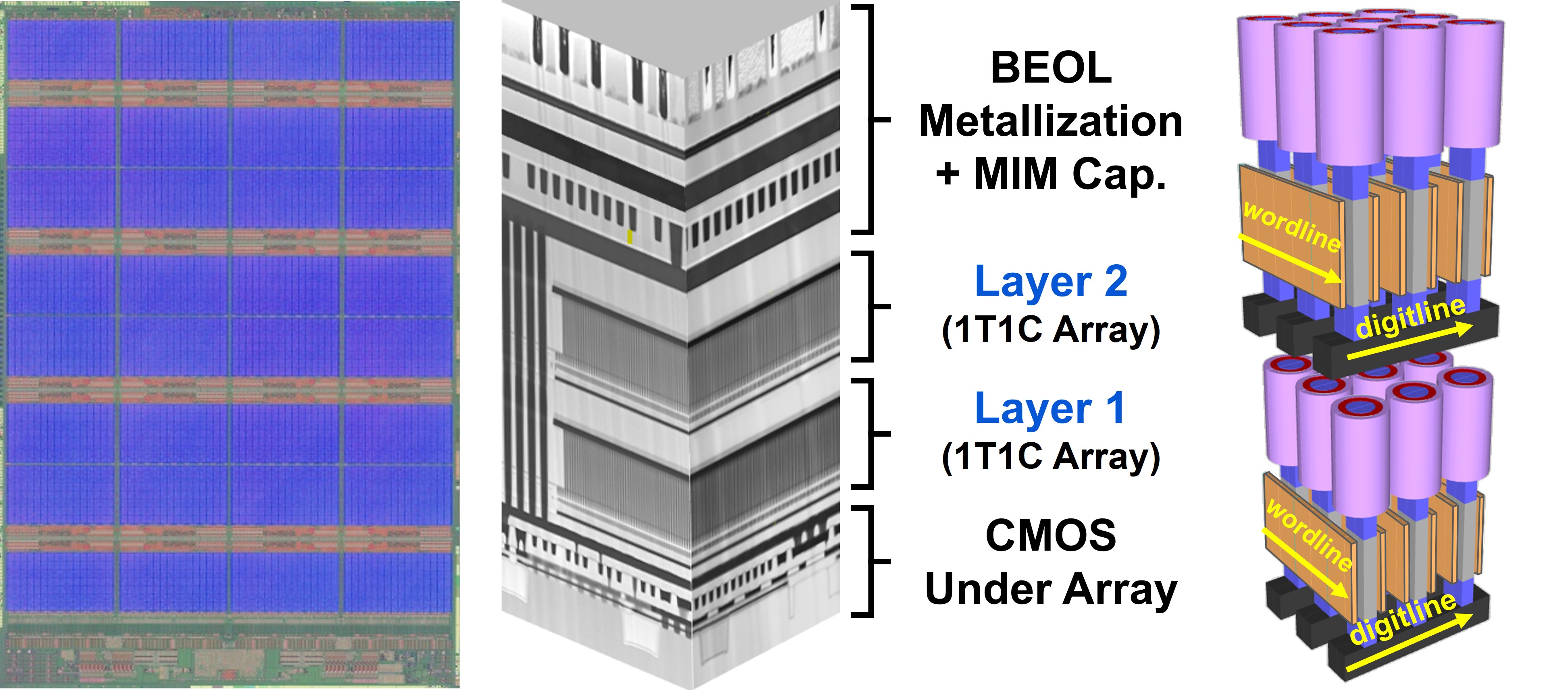
Junmo Lee and colleagues now report a dual-gated non-volatile capacitive memory fabricated on the top metal layer of a foundry CMOS chip. The fabrication process begins with the removal of the chip’s passivation layer, followed by the deposition and patterning of the bottom electrode and interconnects. A layer of hafnium zirconium oxide (HZO) is then deposited using a tungsten sacrificial layer, and a film of tungsten-doped indium oxide (In2O3) grown via atomic layer deposition. The process concludes with the formation of a palladium top electrode and back-end pads, followed by a hafnium oxide (HfO2) top dielectric and then a palladium top gate.
The device exhibits a capacitive on/off ratio of 63.1, endurance exceeding 109 cycles at a read voltage of 1 V and retention of above 104 s at 25 °C. The operational principle of the integrated two-transistor–one-capacitor (2T–1C) device was validated by demonstrating the current amplification behaviour of the capacitance-modulated 40-nm silicon transistor within the integrated structure. Based on the measured data, the researchers proposed and simulated a cell-level digital compute-in-memory circuit model.

The study was also presented at IEDM2025: Technical Highlight – Monolithic 3D Capacitive Memory for Compute-in-Memory:
This joint work by Georgia Tech & TSMC, nominated for Best Student Paper in Emerging Device Technology, describes the first monolithic 3D (M3D) integration of dual-gated non-volatile capacitive memory (nvCAP) with an ALD W-doped In₂O₃ channel on a TSMC foundry 40nm CMOS chip. The novel dual-gate design resolves the long-standing challenges of weak erase and poor retention in oxide-channel ferroelectrics, achieving a record non-destructive on/off ratio of ~64.4 at 0V on a foundry CMOS chip. In addition, the paper introduces a new capacitive digital compute-in-memory (Cap-DCIM) paradigm, showing >140x efficiency improvements versus analog CIMs and >100x lower static power than SRAM-based CIMs, pointing to a scalable and energy-efficient path for future memory-compute integration. The operational principle of M3D Cap-DCIM is experimentally validated by demonstrating BEOL capacitance-modulated FEOL transistor current amplification through the monolithically integrated DG nvCAPs on a foundry CMOS chip.
Paper 28.3, “Monolithic 3D Integration of Dual-Gated ALD Oxide-Channel Non-Volatile Capacitive Memory on 40nm Si CMOS for Digital Compute-in-Memory,” J. Lee et al, Georgia Tech

Source: