Showing posts with label Emerging memory. Show all posts

Tuesday, November 13, 2018

Spin Memory Teams With Applied Materials to Produce a Comprehensive Embedded MRAM Solution

FREMONT, Calif. — Spin Memory, Inc. (Spin Memory), the leading MRAM developer, today announced a commercial agreement with Applied Materials, Inc. (Applied) to create a comprehensive embedded MRAM solution. The solution brings together Applied’s industry-leading deposition and etch capabilities with Spin Memory’s MRAM process IP.


Key elements of the offering include Applied innovations in PVD and etch process technology, Spin Memory’s revolutionary Precessional Spin CurrentTM (PSCTM) structure (also known as the Spin Polarizer), and industry-leading perpendicular magnetic tunnel junction (pMTJ) technology from both companies. The solution is designed to allow customers to quickly bring up an embedded MRAM manufacturing module and start producing world-class MRAM-enabled products for both non-volatile (flash-like) and SRAM-replacement applications. Spin Memory intends to make the solution commercially available from 2019.

“In the AI and IoT era, the industry needs high-speed, area-efficient non-volatile memory like never before,” said Tom Sparkman, CEO at Spin Memory. “Through our collaboration with Applied Materials, we will bring the next generation of STT-MRAM to market and address this growing need for alternative memory solutions.”

“Our industry is driving a new wave of computing that will result in billions of sensors and a dramatic increase in data generation,” said Steve Ghanayem, senior vice president of New Markets and Alliances at Applied Materials. “As a result, we are seeing a renaissance in hardware innovation, from materials to systems, and we are excited to be teaming up with Spin Memory to help accelerate the availability of a new memory.”
About the PSC

Saturday, January 27, 2018

Scaling proven for embedded Super Fast Non-volatile Memory from Dresden

Ferroelectric hafnium oxide and related materials have been developed in Dresden, Germany for over 10 years now. At the IEDM2017 in December Globalfoundries Fab1 and their partners (NaMLab, Fraunhofer and Ferroelectric Memory GmbH) presented their latest results using the Fab1 22nm FDSOI technology with embedded NVM cells embedded as adopted "standard" high-k / metal gate stacks in the front end process module as so called FeFETs.

Previously much of the work was based on Globalfoundries Fab1 28 nm technology so the move to 22 nm really proves that scalig is back to ferroelectric memory technologies as shown on LinkedIn by Prof. Mikolajick (NaMLab) below.. Since the high-k (doped HfO2) is deposited by ALD this technology is scalable also for FinFETs so don´t be surprised if Globalfoundries would soon present also FeFinFETs.

A FeFET based super-low-power ultra-fast embedded NVM technology for 22nm FDSOI and beyond

IEEE Xplore: 25 January 2018 DOI: 10.1109/IEDM.2017.8268425  

Abstract: We show the implementation of a ferroelectric field effect transistor (FeFET) based eNVM solution into a leading edge 22nm FDSOI CMOS technology. Memory windows of 1.5 V are demonstrated in aggressively scaled FeFET cells with an area as small as 0.025 μm2 At this point program/erase endurance cycles up to 105 are supported. Complex pattern are written into 32 MBit arrays using ultrafast program/erase pulses in a 10 ns range at 4.2 V. High temperature retention up to 300 °C is achieved. It makes FeFET based eNVM a viable choice for overall low-cost and low-power IoT applications in 22nm and beyond technology nodes.


Saturday, January 6, 2018

New ALD High-k / 2D MoS2 light-erasable memory suitable for large area manufacturing technology

Phys.Org reports that researchers at the Institute of Microelectronics Chinese Academy of Sciences (IMECAS), and Fudan University have used 2D MoS2 to design a new light-erasable memory.

According to the article in Applied Physics Letter, the memory stack is based on an high-k dielectric stack (Al2O3/HfO2/Al2O3) and an atomically thin MoS2 channel, where he HfO2 act as the charge trapping layer. The holes in the HfO2 charge-trapping layer will tunnel to the MoS2 channel through the 4 nm Al2O3 tunnel layer. 
 
 
Schematic band diagrams of the MoS2/Al2O3/HfO2/Al2O3/Gate structure at (a) flat-band condition, (b) programming operation, and (c) erasing operation. (Supplementary information, Applied Physics Letters. DOI: 10.1063/1.5000552)

"In general, system-on-panel (SOP) describes a new display technology in which both active and passive components are integrated in one panel package, typically on the same glass substrate (sometimes system-on-panel is also named system-on-glass)," coauthor Hao Zhu at Fudan University told Phys.org. "This is different from traditional display technologies such as cathode ray tube (CRT) displays. One major characteristic of SOP is the application of thin-film technology, such as low-temperature poly-silicon (LTPS) thin-film transistor (TFT) arrays on the glass substrate. However, silicon-based thin-film transistors are being replaced by TFTs with new materials with improved properties. The indium gallium zinc oxide (IGZO) or zinc tin oxide (ZTO) thin film mentioned in our paper is also a good example. [Phys.org]

"Currently, we are working on the large-scale integration of such light-erasable 2-D memory devices using programmable light pulses with controllable wavelength and pulse duration," he said. "We are using new material synthesis methods such as atomic layer deposition to grow large-area MoS2 and other 2-D ultra-thin films for circuit-level applications." 
[Phys.org]

The future prospects for large scale manufacturing are there. Except for the MoS2 channel, both Al2O3 and HfO2 are standard ALD processing technologies since more than 10 years in the semiconductor industry and recent developments for flexible OLED Display manufacturing  has made the ALD technology also available for large panel processing and roll to roll technology is just looking for an excuse high volume manufacturing.
 
Article: Long-Fei He et al. "Light-erasable embedded charge-trapping memory based on MoS2 for system-on-panel applications." Applied Physics Letters. DOI: 10.1063/1.5000552

Full story: LINK

Wednesday, November 1, 2017

XPoint NVM Array Process Engineering & Teardown

By Ed Korczynski, Sr. Technical Editor: Now that TECHINSIGHTS has published a teardown of a 3D XPoint array, we have seen cross-section transmission electron micrographs (TEM) of the device. From first principles of process engineering, we can make educated guesses as to the process flows and challenges in creating this type of non-volatile memory (NVM) integrated circuit (IC). Evolution of device technology over more than fifteen years has resulted in cross-point arrays connecting precise stacks of chalcogenide materials. Intel with “Optane” and Micron with “QuantX” branded ICs can now claim success in commercializing what has always looked good in R&D but was notoriously difficult to make in high-volume manufacturing (HVM).

Figure 1 shows the TEM cross-section, parallel to the wordline direction, of a XPoint memory cell array taken from an Intel Optane product. There are two levels of cross-point cell-stacks, connected in the middle by bitlines (orthogonal to the wordlines). The upper- and lower-wordlines have been analyzed as tungsten (W) metal with tungsten-nitride (WN) barriers. The memory cell material is a variant on a germanium-antimony-teluride (GeSbTe or “GST”) chalcogenide glass, while the selector material is made with arsenic-silicon-germanium-selenide.


Fig. 1: Cross-section TEM of Intel XPoint NVM array in the wordline direction, showing two levels of memory cell stacks separated by bitline arrays. (Source: greyscale image by TechInsights, color commentary by Ed Korczynski)

Full article: LINK

Wednesday, June 28, 2017

Formation of BiFeO3 from a Binary Oxide Superlattice Grown by ALD

Drexel University has been developing Bi-Fe-O ferroelecttrics (and others) for many years and here they report on ALD of polycrystalline BiFeO3 thin films on SiO2/Si(001) by ALD using  ferrocene, triphenyl-bismuth, and ozone. Due to its ferroelectric properties BiFeO3 is intersting for future non-volatile memory (FeFETs and FRAM). The ALD of Bi-Fe-O thin films were carried out in a Picosun R200 Advanced Reactor (Supporting Information, for all the process details).


However, iron is not likely to be used in a standard 300mm CMOS fab today, neither in front nor in backend of line - it´s just diffusing to fast to places it is not wanted. But that said, a stand alone memory technology in a dedicated fab may find ways to handle that. The other contender for novel highly scaled ferroelectric metal oxides is the HfO2 based systems researched by NaMLab, Fraunhofer and GloFo in Dresden Germany. Those systems looks much more promising since they are already shuffling leading edge 300 mm wafers since a while now and HfO2 has been in HVM since 2004 (Samsung 90 nm DRAM, HfAlOx MIS stack). The HfO2 ferroelectric R&D has been going on for more than 10 years actually. This just show s how long time materials and device development takes in the semiconductor industry


Formation of BiFeO3 from a Binary Oxide Superlattice Grown by Atomic Layer Deposition


ChemPhysChemEarly View, Version of Record online: 20 JUN 2017
DOI: 10.1002/cphc.201700407

Abstract: By growing alternating layers of Fe2O3 and Bi2O3, we employ a superlattice approach and demonstrate an efficient control of the cation stoichiometry. The superlattice decay and the resulting formation of polycrystalline BiFeO3 films are studied by in situ X-ray diffraction, in situ X-ray photoelectron spectroscopy, and transmission electron microscopy. No intermediate ternary phases are formed and BiFeO3 crystallization is initiated in the Bi2O3 layers at 450 °C following the diffusion-driven intermixing of the cations. Our study of the BiFeO3 formation provides an insight into the complex interplay between microstructural evolution, grain growth, and bismuth oxide evaporation, with implications for optimization of ferroelectric properties.

Tuesday, June 27, 2017

Picosun’s ALD solutions enable non-volatile memories (ReRAM)

As previously reported here (LINK) New prospects for universal memory from MIPT Russia using Picosun ALD: ESPOO, Finland, 27 June, 2017 – Picosun Oy, leading supplier of high quality Atomic Layer Deposition (ALD) thin film coating solutions, reports of breakthrough results achieved with its ALD technology in development of novel high-speed memories. These memories are required in state-of-the-art data storage applications, where a combination of very large capacity and extremely fast operating speed is needed. The results have been obtained at Picosun’s long-term customer Moscow Institute of Physics and Technology (MIPT), Russia.


Experimental cluster, including a Picosun ALD reactor, for growing and studying thin films in a vacuum at the Center of Shared Research Facilities, MIPT

ReRAM (Resistance Switching Random Access Memory) is a new, non-volatile memory type which has the attributes to become the much sought-after universal memory to replace and outperform the current technologies, and to solve the ever-growing demand for more and more efficient data storage systems. ReRAM is fast, small, structurally simple, it has high capacity and it operates at low voltages. These features help to decrease the device size, power consumption, and response time, allowing yet smoother-operating electronic end products. Smaller operating voltage enables ReRAM integration also to low-power devices such as portable, wearable, and mobile electronics, remote sensing and IoT (Internet of Things) applications, the number of which is growing explosively at the moment.

Friday, June 23, 2017

Yole Développment is releaseing the Emerging Non-Volatile Memory 2017 June 28

Yole Développment: The key emerging non-volatile technologies like phase-change memory (PCM), magnetoresistive random access memory (MRAM) and resistive random access memory (RRAM) have long development histories. Yet, their adoption remains restricted to niche markets due to various factors. Available products have limited density, and the introduction of high density products by emerging NVM pioneers has been delayed. There are manufacturing challenges due to the introduction of new materials and process steps. Meanwhile, mainstream memory technologies are continuously improving in terms of density and cost. Finally, there has been an absence of a killer application that would challenge dynamic random access memory (DRAM) and NAND flash memory. [read further, LINK] - Thanks to Terry Francis for sharing this one!

 Time to market for differen memory technologies  (Yole Développment, LINK)

Unfortunately, Yole does not mention here the developments in Ferroelectric hafnium oxide based FeFET and FRAM (by NaMLab, Fraunhofer and Globalfoundries). There has been quite some progress over a 10 years development (originally imitated and discovered by Qimonda R.I.P.) so far and most recent approach by Imec integrating Ferro FETs in a bit scalable 3D-NAND style architecture. The main advantage of this technology is that in the case of a logic embedded memory cell and a stand alone 3D-NAND style version standard equipment and process flows can be used in HVM. In addition, according to Imec memory Guru Jan van Houdt, "It [FeFETs] has particularly interesting characteristics for future storage-class memory, which will help overcome the current bottleneck caused by the differences in speed between fast processors and slower mass memory"

The last couple of years there is an increased IP filing in hafnium oxide and related technologies and precursors and especially for ferroelectric memory. It was also apparent by studying the last VLSI program that there are man more mature activities in this technology and if I remember correctly there was 6-8 presentations on this topic. Possibly the report itself gives some insights also to the status of ferroelectric NVM technologies.

 
Imec is confident that their FeFET concept has all the required characteristics for both stand-alone and embedded memories, from non-volatile DRAM to Flash-like memories. (2017 Symposia on VLSI Technology and Circuits, Kyoto Japan June 7, 2017, source www.imec.be) 
 

Sunday, June 18, 2017

New prospects for universal memory from MIPT Russia using Picosun ALD

MIPT Reports: Researchers from MIPT’s Center of Shared Research Facilities have found a way to control oxygen concentration in tantalum oxide films produced by atomic layer deposition. These thin films could be the basis for creating new forms of nonvolatile memory.

The MIPT non-volatile ReRAM memory cell is based on ALD deposited tantalum oxide using tantalum ethoxide and water.

“The hardest part in depositing oxygen-deficient films was finding the right reactants that would make it possible to both eliminate the ligands contained in the metallic precursor and control oxygen content in the resulting coating,” says Andrey Markeev, who holds a PhD in physics and mathematics and is a leading researcher at MIPT. “We achieved this by using a tantalum precursor, which by itself contains oxygen, and a reactant in the form of plasma-activated hydrogen.”

Experimental cluster, including a Picosun ALD reactor, for growing and studying thin films in a vacuum at the Center of Shared Research Facilities, MIPT

Wednesday, June 7, 2017

Another breakthrough in CMOS-compatible ferroelectric memory

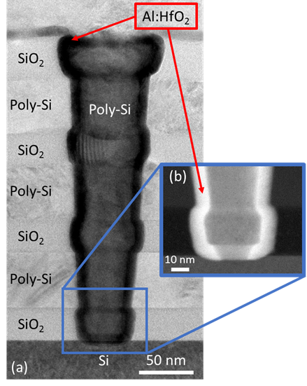
Imec, the world-leading research and innovation hub in nanoelectronics and digital technology, announced today at the 2017 Symposia on VLSI Technology and Circuits the world's first demonstration of a vertically stacked ferroelectric Al doped HfO2 device for NAND applications. Using a new material and a novel architecture, imec has created a non-volatile memory concept with attractive characteristics for power consumption, switching speed, scalability and retention. The achievement shows that ferro-electric memory is a highly promising technology at various points in the memory hierarchy, and as a new technology for storage class memory. Imec will further develop the concept in collaboration with the world's leading producers of memory ICs.

Full story : LINK

Friday, October 28, 2016

Ferroelectric memory startup aims at GloFo's 22FDX at Fab1 in Dresden

Here is good and promising news about the Ferroelectric Mmeorz Company (FCM) in Dresden (as published by EE Times):
 
TEM of FeFET processed in 28 nm high-k metal gate CMOS Technology (left) and 2D TCAD-model for device simulation (right). (Picture from NaMLab)
 
The company, a spin-off from the nano- and micro- laboratory (NaMLab) at the Technical University of Dresden, is making use of the recently discovered ferroelectric effect in silicon-doped hafnium dioxide. The company has made progress over the last year in terms of establishing hafnium ferroelectric memory as design choice for embedded nonvolatile memory in 28nm processes and below. 

The 64kbit active array was developed with Globalfoundries Inc. and is the subject of a paper due to be presented at the upcoming International Electron Devices Meeting (IEDM) in San Francisco in December. Meanwhile FMC is seeking funds. Having received more than €4 million (about $4.4 million) in government grants the company says it is looking approximately €2 million more Series A funding round.

Continue reading in EE Times about FCM here: 

Ferroelectric memory startup aims at GloFo's 22FDX

Electronics EETimes (registration)-vor 20 Stunden
The company, a spin-off from the nano- and micro- laboratory (NaMLab) at the Technical University of Dresden, is making use of the recently ...

Dresden Memory Startup To Debut At Semicon Europa

EE Times-15.09.2015
The company is the product of work at NaMLab on the ferroelectric effect in thin films of silicon-doped hafnium dioxide. That work was, in turn, ...

Wednesday, October 26, 2016

UPDATE : Transition metal compounds, Belux2 - 17-18 November 2016 - imec Belgium

Registration for the workshop is still open: http://www2.imec.be/be_en/education/conferences/belux2.html. Many of imec's large industrial IDM partners and equipment suppliers have registered for this workshop - an excellent opportunity to meet the experts in this field!

 
Imec and the COST action HERALD will host a workshop dedicated to Transition metal compounds driving technological advancement. The Belux2 workshop will take place at imec in Leuven, Belgium on 17-18 November 2016.

 This 2 half-day workshop will provide an excellent opportunity to spark multidisciplinary discussions regarding the modeling, deposition and characterization of novel transition metal compounds for next generation technologies.

The program will consist of Presentations by invited speakers.
  
Prof. Atsufumi Hirohata (University of York, UK) - Heusler Alloy Films for Spintronic Devices
Dr. Stanislav Chadov (Max Planck, Germany) - Room-temperature tetragonal noncollinear antiferromagnet: Pt2MnGa
Prof. Andreas Michels (University of Luxembourg, Luxembourg) - Magnetic Neutron Scattering Studies on Nd-Fe-B Magnets
Prof. Thibault Devolder (Universite Paris Sud, France) - Nanosecond-Scale Switching in Perpendicularly Magnetized STT-MRAM Cells
Prof. Jens Kreisel (Luxembourg Institute of Science and Technology, Luxembourg) - Strain & phase transitions in oxide heterostructures and ultrathin films
Prof. Sebastiaan van Dijken (Aalto University, Finland) - Electric-Field Control of Magnetism in Multiferroic Heterostructures
Prof. Guus Rijnders (University of Twente, The Netherlands) - Piezeoelectrics
Geoffrey Pourtois (imec, Belgium) - Modeling of the impact of the chemical environment on the properties of MX2 materials for nanoelectronic applications
Stephen McDonnell (University of Virginia, US) - Deposition of and on 2D materials
Dr. Ageeth Bol (Eindhoven University, The Netherlands) - Atomic layer deposition of metals and oxides on graphene for future nanoelectronics
Prof. Alexander Shluger (University College London, UK) - Some ideas on the mechanisms of electroforming in oxides from DFT simulations
Dr. Uwe Schroeder (Namlab, Germany) - HfO2 and ZrO2 based ferroelectric materials for non-volatile memory applications
Prof. Matthias Wuttig (RWTH Aachen, Germany) - Novel Phase Change Materials by Design: The Mistery of Resonance Bonding
Dr. Ilia Valov (FZ Juelich, Germany) - Interfaces, Mobile Ions and Moisture Effects in ReRAM memristive systems
·         Poster session.
  • Walking dinner.
More information and the registration form are available at: http://www2.imec.be/be_en/education/conferences/belux2/home.html.
The fee for the workshop is only 50 euro (VAT included). The deadline for registration is 11 November 2016.
Poster contributions are welcome by abstract submission (http://www2.imec.be/be_en/education/conferences/belux2/call-for-papers.html). The deadline for abstract submission is 4 November 2016.
We really look forward to welcoming you at imec!
Best regards from the Belux2 organizing committee.
Naoufal Bahlawane, Luxembourg Institute of Science and Technology (LIST)
Sven Van Elshocht, imec (chairman)
Christoph Adelmann, imec
Annelies Delabie, imec
Johan Swerts, imec
Kathleen Vanderheyden, imec
Fred Loosen, imec
Please forward this email to whom it may concern.
http://www2.imec.be/content/user/Image/events/HERALD-LOGO-(PRIMARY).png
http://www2.imec.be/content/user/Image/events/logo_cost.png

Monday, October 24, 2016

Video interview with Er-Xuan Ping of Applied Materials on Emerging memories and the new material


Here is a very interesting video interview by G Dan Hutcheson (weVISION) with Er-Xuan Ping, from Applied Materialson emerging memory and the materials to make them. Thanks to Terry Francis for sharing this one!

Emergent memories and the new materials needed to make them ... a conversation with Er-Xuan Ping of Applied Materials


[VIDEO LINK] Abstract: Emergent semiconductor memory technologies are finally breaking out of lab and getting into the fab. Non-volatile 3D NAND with its vertical memory stacks is reaching computers and data centers in volume. Intel and Micron’s 3D Xpoint™ is started its volume production ramp in 2016 and headed to a data center near you. Embedded MRAM is now on the major foundries roadmaps. Each of these technologies has required significant breakthroughs in materials technology. Some new materials are not friendly to manufacturing, so ways to process them had to be worked out. In other cases, such as the selector in 3D Xpoint, materials had to be developed that could withstand the infinite switching life requirements as these non-volatile memory cells got close to the processor. They also had to deal with changes in the physics, such as the adoption of space-charge. The same has been true for VNAND, where charge-trap technology is used in favor of the more conventional floating gate memory cells used in planar NAND. New materials have also come to the rescue for DRAMs, which continue to need planar shrinks. We find out why this is happening and what is needed in this conversation with Er-Xuan Ping, from Applied Materials (AMAT), where he’s Managing Director of Memory and Materials Technologies in the Advanced Product and Technology Development Group. He has previously held positions at Sandisk and Micron Technology. Dr. Ping holds a Ph.D. in electrical engineering from Iowa State University.

Wednesday, October 12, 2016

HP reports low energy Memristor precisely tuned by ALD

Nanotechweb reports: Researchers at Hewlett Packard Labs in California, the University of Massachusetts Amherst and Seoul National University are reporting on a new low-current, self-rectifying memristor made from titanium ion electron traps in a niobium oxide matrix. The device might be used as an embedded memory on low-power chips and for storing data in Internet of Things (IoT) appliances.
 
 
The memristor device (Pt/NbOx/TiOy/NbOx/TiN) is based on titanium ion electron traps in a niobium oxide (NbOx) matrix deposited by ALD. ALD allows control of the sub-atomic monolayers in the structure and so precisely control how the Ti traps are distributed in the NbOx matrix. (Figure from Nanotechweb.org)
 
According to the team, led by Stanley Williams, also of Hewlett Packard Labs, the new memristor could be used to make embedded memories for low-power chips, such as ASICS. “Since the technology is fully CMOS compatible, it might also be used to store data in or near sensors at the edge of IoT devices,” says Kim. “Eventually, it might find use as a stand-alone non-volatile memory for low-power systems.”

Saturday, May 21, 2016

Presentations from NCCAVS Meeting on Advanced Memory availaable for Download


Recently (April 21, 2016) The North California Chapter of The American Vacuum Society (NCCAVS) Thin Film User Group organized a meeting on Advanced Memory in San Jose, California. Now all the presentations by Intel, Globalfoundries and Avalanche Technology are now available for download at the TFUG Proceedings page

The Thin Film Users Group (TFUG) focuses on state-of-art thin-films deposition and applications for semiconductor and related fields, such as nanotechnology, renewable energy, imaging devices, design for manufacturing, and advanced memory research. It is composed of engineers and scientists from device manufactures, semiconductor equipment venders and universities. The TFUG's main activity is a bi-monthly half-day open seminar from researchers and industry technologists with technical presentations on topics of current interests.
 
This event was chaired by Chakku Gopalan (Intel Corporation), Co-chared by Chari Perera (Applied Materials Deposition Products Group), Paul Werbaneth (Intevac, Inc.) and Michael Oye (UCSC).

NAND Flash: Where are we, where are we going?

Pranav Kalavade, Principle Engineer at Intel, Non-volatile Memory Solutions Group, Santa Clara.

NAND Flash: Where are we, where are we going? (471k pdf)

Emerging Memory: From Technology to Applications

Dave Eggleston, Vice President of Embedded Memory at GLOBALFOUNDRIES

Emerging Memory: From Technology to Applications (3.5MB pdf)


STT MRAM Technology and Productization

Jing Zhang, Ph.D., Sr. Director of Product Development at Avalanche Technology

STT MRAM Technology and Productization (2.1MB pdf)


CBRAM for IoT applications

Nathan Gonzales, Adesto Technologies


Monday, April 4, 2016

New Critical Materials Conference's Powerful Agenda


 Buy Reports  | CMC Fabs   |  CMC Conference  |  Register Now
New Critical Materials Conference's Powerful Agenda
May 5-6, Hillsboro Oregon
The Critical Materials Conference provides a framework to catalyze the flow of "actionable" technical and supply chain information related to critical materials. 

New Additions to the Critical Materials Conference Include: 
  • David Thompson, Ph.D., Director of Process Chemistry of Applied Materials
    • Agony in New Material Introductions - Minimizing and Correlating Variabilities
  • Suresh Ramalingam, Sr. Director, Advanced Packaging Development of Xilinx
    • Packaging Materials - Future Challenges 
A highly differentiated program, with networking opportunities for all attendees. 
For full agenda details click here.

Themes of the Conference are centered around the needs of the Critical Materials Council and the global IC fabrication industry. While executive conferences typically focus on the "what" and "why" of materials technologies, this conference will discuss "how" new materials can be controllably, safely, and cost-effectively used in fabs. The Conference will also include market data to validate "when" materials will be needed. Attendees from fabs, OEMs, and materials suppliers alike will have the opportunity to interact with the presenters and colleagues, to gain insights into best-practices of the entire supply-chain.
 
For more information on the conference go to www.cmcfabs.org/seminars/ 
Great Sponsorship Opportunities available, 
please contact cmcinfo@techcet.com or call 1-480-382-8336

Sponsors and Committee

Thursday, January 7, 2016

The Critical Materials Council to be managed by TECHCET in 2016

 The Critical Materials Council for Semiconductor Fabricators, originally established by ISMI/SEMATECH in the early 1990’s, will be managed by TECHCET CA LLC starting January 01, 2016. Under its new name CMC Fabs, the membership-based organization of semiconductor fab & fabless manufacturers will continue working to identify and remediate issues impacting the supply, availability, and accessibility of both current and emerging semiconductor process materials. In keeping with SEMATECH tradition, the work of the international council takes place in a non-competitive environment for the benefit of the semi device fabrication community. Topics addressed are identified and prioritized by the member companies.


The organization has a new website at cmcfabs.org, which includes an overview of the Council’s mission, news of upcoming events and a Members Only portal for access to minutes of monthly phone/WebEx meetings and workshop details. The site also features access for Members to the TECHCET Critical Materials Reports and the related quarterly updates.

The next face-to-face meeting of CMC Fabs will take place May 3-6, 2016 in Hillsboro, Oregon. The meeting will include the annual CMC Materials Seminar held on May 5-6 that is open to the public. Sessions include a market briefing, supply chain issues and methods, the evolution of emerging materials in ALD / ALE, and the materials revolution around carbon. Speakers will be drawn from fabs, suppliers and analysts to address topics of concern and interest to the Council, and the semiconductor materials supply chain.


CMC Fabs is a unit of TECHCET CA LLC, a firm focused on Process Materials Supply Chains, Electronic Materials Technology, Materials Market Research and Consulting for the Semiconductor, Display, Solar/PV, and LED Industries. The company has been responsible for producing the SEMATECH Critical Material Reports since 2000.

Wednesday, December 16, 2015

LaAlO3/STO interface with a Chemically Switchable Ultraviolet Luminescence

A new effect discovered at Drexel University of a material stack that could be used to relay information between molecules by UV light like in a memory chip but with the significant advantage of doing it without an electric current.

"While studying a sample of lanthanum aluminate film on a strontinum titanate crystal, the team, led by Drexel College of Engineering Professor Jonathan E. Spanier, Andrew M. Rappe, from Penn; Lane W. Martin, from Berkeley and Temple's Xiaoxing Xi, discovered that the sample was beginning to emit intense levels of UV light. Carefully reproducing the experimental conditions helped them realize that water molecules might be playing a role in the UV light being emitted from inside the material."


In the presence of a water molecule on its surface, lanthanum aluminate film on a strontium titanate crystal emits ultraviolet light from its interior (Drexel University).

Tuesday, December 1, 2015

IBM TJ Watson Research to present an ALD Ge-Sb-Te Phase Change Material at IEDM 2015

IBM TJ Watson Research to present an ALD Ge-Sb-Te Phase Change Material at IEDM 2015.

Crystalline-as-Deposited ALD Phase Change Material Confined PCM Cell for High Density Storage Class Memory, M. BrightSky, N. Sosa, T. Masuda*, W. Kim, S. Kim, A. Ray,  R. Bruce, J. Gonsalves,  Y. Zhu, K. Suu*, and C. Lam, IBM TJ Watson Research, *ULVAC
We show a robust 4:1 aspect ratio 33nm diameter confined PCM cell which utilizes an in-situ metal nitride liner plus nano-crystalline-as-deposited ALD Ge-Sb-Te phase change material. We report a programming endurance of beyond 1E10, 80ns 10x switching, and a path towards a high density PCM suitable for Storage Class Memory.
Memory Technology PCRAM and Flash: http://ieee-iedm.org/session-3-circuit-device-integration-advanced-cmos-technology-platform/


TSMC to present 16nm FinFET embedded HfO2 ReRAM at IEDM2015

According to Semconductor Engeneering, TSMC is to present a NVM 16nm FinFET embedded ReRAM at IEDM2015 using basically a standard ALD HfO2 High-k / Mettal Gate Stack. Assumingly, TSMC just run also here the standard ASM Pulsar HfCl4/H2O thermal ALD process like for the gate dielectric. The novel device integration is denoted FIND RRAM. Interesting here is a comparison with NVM 28nm Ferroelectric FeFET using also HfO2 in development by Globalfoundries, NaMLab, Fraunhofer and FMC, which is normally done using the ASM Pulsar process but has also been proven using other ALD Chambers and  precursors.Especially in the case of a 3D FRAM integration where typically HfCl4 is difficult. However, as far as I know these guys have yet not published a FinFET FeFET version, which should be pretty straightforward unless the rather thick HfO2 (6-10 nm) that is needed to get a ferroelectric phase of HfO2 proves difficult to integrate and especially pattern (dry etch or CMP).

ReRAM Gains Even More Steam. The prospect of using the latest in finFET processing to enable embedded non-volatile memory (NVM) will be described by a team from TSMC and Tsing Hua University in Taiwan at the IEDM meeting on Dec. 8 in Washington, D.C.


Fin in structured memory cell, from IEDM paper abstract. The fin consists of a multilayer sandwich of TiN/ HfO2/SiO2 with the finFET metal gate and epi SiP as the two electrodes.  

Here is some previous published material from EETimes Europe on this technology and the abstract below form the IEDM Memory RRAM session.

1Kbit FINFET Dielectric (FIND) RRAM in Pure 16nm FinFET CMOS Logic Process, H.-W. Pan, K.-P. Huang, S.-Y. Chen, P.-C. Peng, Z.-S. Yang, K.-H. Chen*, Y.-H. Kuo*, C.-P. Lin*, B.-Z. Tien*, T.-S. Chang*, C.-H. Kuo*, Y.-D. Chih*, Y.-C. King, and C.J. Lin, National Tsing Hua University, *Taiwan Semiconductor Manufacturing Company
A fully CMOS process compatible FinFET Dielectric RRAM (FIND RRAM) is firstly proposed and demonstrated by 1kbit RRAM macro on 16nm standard FinFET CMOS logic platform. The new 16nm low voltage FIND RRAM consists of one FinFET transistor for select gate and an HfO2-based resistive film for a storage node of the cell. The FIND RRAM largely improves the set and reset characteristics by the locally enhanced field at fin corners and results in a low set voltage and reset current in array operation. Besides, by adopting the 16nm FinFET CMOS logic process, the FIND RRAM is shrink to an aggressive cell size of 0.07632um2 without additional mask or process step. The low voltage operation, excellent reliability, and very stable LRS/HRS window are all realized in the new fabricated 1kbit macro. They all support the new FIND RRAM technology is a promising embedded NVM in the coming FinFET era.


As comparison, a TEM of FeFET processed in 28 nm high-k metal gate CMOS Technology (left) and 2D TCAD-model for device simulation (right). (Picture from NaMLab)