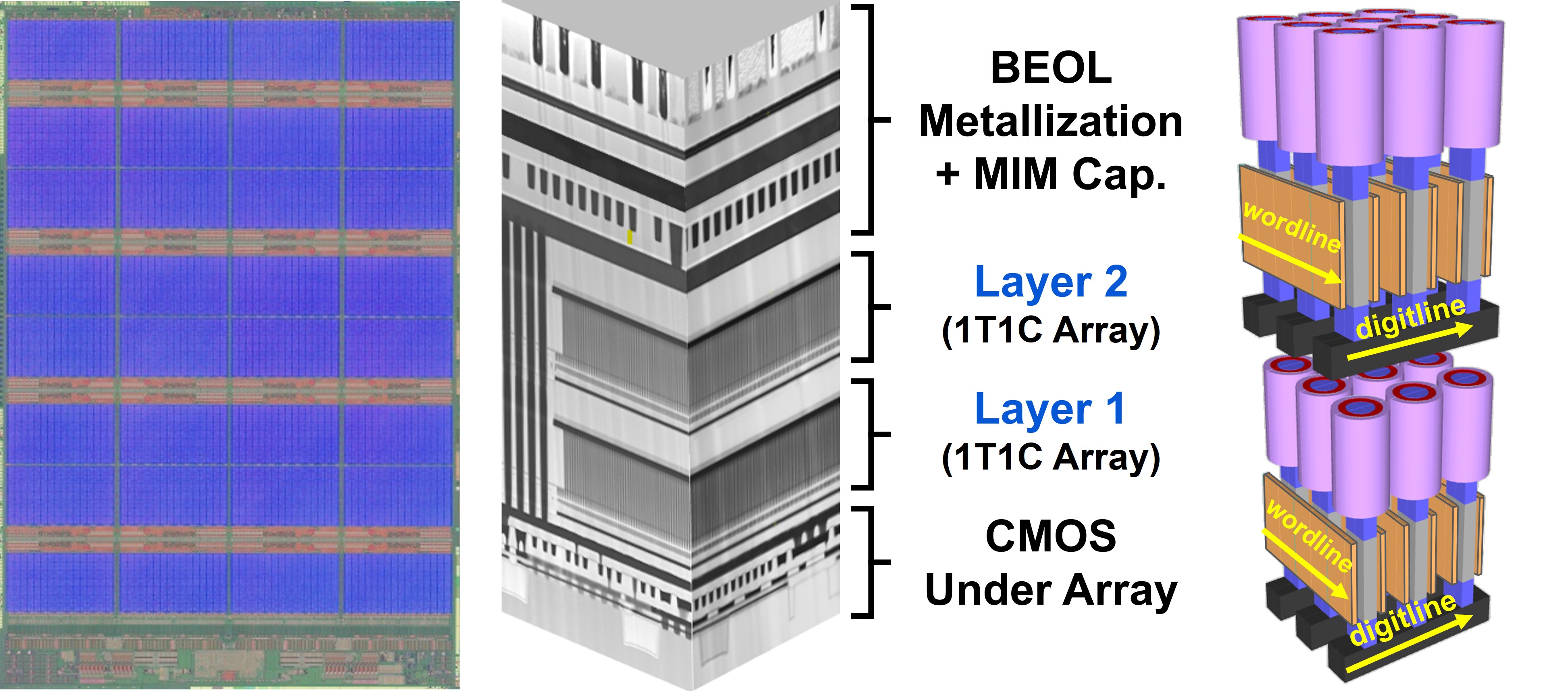
Saturday, January 20, 2024
Revolutionizing CPU Memory: How ReRAM is Shaping the Future of High-Bandwidth Applications
Wednesday, October 18, 2023
Micron Unveils Breakthrough NVDRAM: A Dual-Layer 32Gbit Non-Volatile Ferroelectric Memory with Near-DRAM Performance
Monday, September 25, 2023
NEO Semiconductor Unveils Revolutionary 3D NAND and DRAM Innovations at Flash Memory Summit 2023
NEO Semiconductor, known for its expertise in 3D NAND flash and DRAM technologies, presented groundbreaking innovations at Flash Memory Summit 2023 in August. The full presentation can be seen on Youtube (below). CEO Andy Hsu's keynote introduced their latest creation, 3D X-DRAM™, designed to overcome DRAM's capacity limitations and replace 2D DRAM. This technology utilizes the existing 3D NAND flash process with minor modifications, streamlining development and reducing costs. Hsu also unveiled a new AI application, "Local Computing," promising a substantial enhancement in AI chip performance.
X-DRAM™ significantly reduces data latency and provides ultra-high data throughput to unleash the full potential of High-Bandwidth Memory (HBM). HBM uses many Through Silicon Via (TSV) to increase I/O bandwidth. However, the HBM data latency remains almost the same when using conventional DRAM because bit line lengths remain the same.
Furthermore, NEO Semiconductor showcased various novel memory structures derived from 3D X-DRAM™, tailored for applications like 3D NOR flash memory, 3D Ferroelectric RAM (FFRAM), 3D Resistive RAM (RRAM), 3D Magnetoresistive RAM (MRAM), and 3D Phase Change Memory (PCM). These innovations enable the transition from 2D to 3D memory cells.
Hsu underscored the significance of these technologies for the semiconductor industry, cloud providers, and enterprises, highlighting that 3D X-DRAM™ offers a high-speed, high-density, cost-effective, and high-yield solution.
The presentation addressed the challenges faced by DRAM and NAND flash memory in the context of AI applications and introduced two innovative solutions – 3D X-DRAM™ and 3D X-NAND™.
Being part of the prestigious Flash Memory Summit, NEO Semiconductor showcased its technologies at booth number 215, and interested parties had the opportunity to schedule meetings with the company at the event.
In summary, NEO Semiconductor unveiled groundbreaking advancements in 3D NAND flash and DRAM technologies at Flash Memory Summit 2023, offering solutions to critical challenges in memory performance and capacity.
Wednesday, June 28, 2023
New Reconfigurable Logic System Achieved with Heterojunction Transistors using ALD
Korean scientists have created a new kind of logic system using special transistors called H-MTR (Link). These transistors can control negative transconductance (NTC) characteristics, allowing for precise logic operations. By programming the transistors, they can switch between different transfer curves, making them highly versatile.
Using the H-MTR transistors, researchers developed a reconfigurable logic inverter called R-inverter (Link). This inverter performed exceptionally well, with a high static noise margin of 85% for binary logic and 59% for ternary logic. It also showed long-term stability and endurance. This reconfigurable logic system opens up new possibilities for computing methods and can generate different output sequences for the same input signal.
The study also demonstrated a dynamic logic conversion-in-memory by connecting a chain of R-inverters. This method allowed for the generation of three different output sequences using a single input signal. This innovative approach to logic computing has never been seen before. The development of this reconfigurable logic system has great potential for applications in artificial intelligence, integrated circuits, and personalized IoT devices. It addresses the need for compatibility and improved information processing capabilities.
One of the key technologies employed in the development of these reconfigurable logic devices is Atomic Layer Deposition. ALD is a precise thin-film deposition technique that allows for the controlled deposition of atomic layers onto a substrate. In the case of the H-MTR transistors, ALD was used to create the necessary heterojunctions and floating gates with high precision. This enables the fine-tuning of the transistor characteristics and ensures reliable performance. The use of ALD in fabricating these devices highlights the significance of advanced manufacturing techniques in pushing the boundaries of electronic systems and opens up possibilities for further advancements in the field of reconfigurable logic.
A reconfigurable binary/ternary logic conversion-in-memory based on drain-aligned floating-gate heterojunction transistors
Nature Communications volume 14, Article number: 3757 (2023)
Friday, May 7, 2021
Applied Materials MEMORY MASTER CLASS 2021 - slide deck
I missed this opportunity, however, I am grateful for Lita Shon-Roy just sending me the link to the slide deck - Tack så mycket.
Slide deck for the Memory Class LINK
Next class up is Logic June 16, 2021 followed by more interesting topics in 2nd half 2021:
- Specialty semiconductors
- Heterogeneous design and advanced packaging
- Inspection and process control
You are welcome to contact us at TECHCET (jsundqvist@techcet.com) to dig further into the future surge of materials to realize the data-driven economy:
- ALD/CVD precursors
- Metals/PVD Targets
- Photoresist
- Wet chemicals
- CMP pads & slurries
- Bulk, Rare and Speciality gases
- Wafers
Tuesday, February 9, 2021
Capacitorless DRAM using oxide semiconductors could be built in 3D layers above a processor’s silicon
Friday, July 3, 2020
ALD Hafnium oxide as an enabler for competitive ferroelectric devices
Tuesday, July 16, 2019
Endura Impulse - Applied Materials’ New Memory Machines
Tools designed to rapidly build embedded MRAM, RRAM, and phase change memories on logic chips expand foundry options
Applied Materials' Endura Impulse uses nine physical vapor deposition systems to rapidly build RRAM or PCRAM. Photo: Applied Materials
Wednesday, June 19, 2019
TechInsights’ Logic, NAND, DRAM and Emerging Memory Process Roadmaps are here
TechInsights’ technology roadmaps show you the innovations we are monitoring
We constantly monitor the consumer electronics market to determine which manufacturers are planning to release new solutions, and when. We maintain and regularly update technology roadmaps in several different areas: Logic, NAND Flash Memory, DRAM, Emerging Memory, and Internet of Things Connectivity Systems on Chips, and more.
Updates to the roadmaps shown below are released throughout the year; check this page for updates.
Tuesday, May 7, 2019
Applied Materials - The AI Era is Driving Innovations in Memory
The previous computing eras—Mainframe/Minicomputer, PC/Server and Smartphone/Tablet—all benefitted from advances in Moore’s Law whereby 2D scaling was accompanied by simultaneous improvements in performance, power and area/cost—also called “PPAC.”
While AI Era applications are booming, Moore’s Law is slowing; as a result, the industry needs breakthroughs beyond 2D scaling to drive PPAC in new ways. Specifically, we need new computing architectures, new materials, new structures—especially area-saving 3D structures—and advanced packaging for die stacking and heterogeneous designs.
Performance and power are important in the cloud and in the edge, and innovations in memory can help. One approach using existing memory technologies is “near memories” whereby large amounts of working memory are condensed, placed in close physical proximity to logic, and connected via high-speed interfaces. As examples, 3D stacking and through-silicon vias are gaining traction. One major drawback of SRAM and DRAM as “working memories” in these applications is that they are volatile and need a constant supply of power to retain data—such as weights.
To reduce power in the cloud and edge, designers are evaluating new memories that combine high performance with non-volatility so that power is only needed during active read and write operations. Three of the leading new memory candidates are magnetic random-access memory (MRAM), phase-change RAM (PCRAM) and resistive RAM (ReRAM).
Sunday, December 30, 2018
Weebit Nano partners with Indian Institute of Technology Delhi on ReRAM Research
Friday, November 23, 2018
CMC Conference Call for Papers, April 25-26, 2019 in Saratoga Springs, NY, USA
Thursday, November 22, 2018
UMass Engineers Make Crossbar Arrays of the Smallest Memristors
“This work will lead to high-density memristor arrays with low power consumption for both memory and unconventional computing applications,” says Xia. “The working circuits have been made with technologies that are widely used to build a computer chip.”
Understanding the scale of this work is important, Xia says. One nanometer (nm) is one billionth of a meter. The diameter of a human hair is about 100 micrometers, or 100,000 nanometers. Two nanometers are just a few atoms wide. A crossbar is a matrix of tiny switches.
In the Nature Nanotechnology paper, Xia’s research team explains that organizing small memristors into high-density crossbar arrays is critical to meet the ever-growing demands in high-capacity and low-energy consumption, but is challenging because of difficulties in making highly ordered and highly conductive nanoelectrode arrays. The team has addressed this challenge by developing “nanofins,” metallic nanostructures with very high height-to-width ratio and hence vastly reduced resistance, as the electrodes.
This research is an outgrowth of Xia’s 2013, five-year, $400,000 grant from the National Science Foundation (NSF) Faculty Early Career Development (CAREER) Program to develop emerging nanoelectronic devices. Xia’s NSF research has been addressing the biggest obstacle for the continued operation of Moore’s Law, which states that the number of transistors on integrated circuits doubles approximately every two years.
“It (Moore’s Law) worked perfectly for more than 40 years, but now we’re reaching its fundamental limit, due to the quantum effects related to electron flow,” says Xia. “So, we absolutely need new devices that can do a better job.” In addition to Xia, the other authors of the Nature Nanotechnology paper are Shuang Pi, Can Li, Hao Jiang, Weiwei Xia, Joshua Yang and Huolin Xin
Saturday, November 17, 2018
Researchers from University of Groningen, the Netherlands confirm ferroelectricity in nanosized HfO2 crystals
Figure shows inside view of vacuum chamber in which the process of 'pulsed laser deposition' takes place, used to create the hafnium oxide crystals in this study. On the left the glowing substrate on which the film is growing with atomic control; in the center the blue plasma of ions that is created by shooting a laser on a target with the right chemical composition (target visible on the right side of the figure). | Photo Henk Bonder, University of Groningen
Ferroelectric materials have a spontaneous dipole moment which can point up or down. This means that they can be used to store information, just like magnetic bits on a hard disk. The advantage of ferroelectric bits is that they can be written at a low voltage and power. Magnetic bits require large currents to create a magnetic field for switching, and thus more power. However, according to the scientific community, the aligned dipoles in ferroelectric materials are only stable in fairly large groups; thus, shrinking the crystals results into the loss of dipole moment obstructing ferroelectricity based storage devices.
Nevertheless, eight years ago, the first publication by ex-Qimonda experts and researchers from Fraunhofer and RWTH Aachen (Appl. Phys. Lett. 99, 102903 (2011); https://doi.org/10.1063/1.3634052) announced that hafnium oxide thin films were ferroelectric when thinner than ten nanometres and that thicker films actually lost their ferroelectric properties. This triggered many groups across the globe to dig deeper and confirm the claim of researchers from NamLab. Noheda and her group at University of Groningen was also one of them. Since the ferroelectric hafnium oxide samples used in the study carried out at NaMLab were polycrystalline and showed multiple phases, obscuring any clear fundamental understanding of such an unconventional phenomenon, Noheda and her group decided to study these crystals by growing clean (single-phase) films on a substrate.
Using X-ray scattering and high-resolution electron microscopy techniques, the group observed that very thin films (under ten nanometres) grow in an entirely unexpected and previously unknown polar structure, which is necessary for ferroelectricity. Combining these observations with meticulous transport measurements, they confirmed that the material was indeed ferroelectric. Surprisingly, they noticed that the crystal structure changed when the layers exceeded 10 nm, thus reaching the same conclusion as of the Namlab.
In the substrate that UG researchers used, the atoms were a little bit closer than those in hafnium oxide which strained hafnium oxide crystals a little. Moreover, at a very small size, particles have a very large surface energy, creating pressures of up to 5 GPa in the crystal. This altogether forces a different crystal arrangement and in turn polar phase in the HfO2 film.
One contradicting finding of the UG researchers is that the HfO2 crystals do not need a ‘wake-up’ cycle to become ferroelectric. The thin films investigated at NamLab turned ferroelectric only after going through a number of switching cycles (wake-up cycles) needed to align the dipoles in “uncleaned” samples grown via other techniques. In case of the pulsed laser deposition setup and the substrate used at UG, the alignment is already present in the crystals.
Meanwhile, NaMLab has explored ferroelectric properties in atomic layer deposition (ALD) based thin-films of doped HfO2, and has achieved revolutionary results (LINK). A variety of dopant materials (Si, Al, Ge, Y, Gd, La and Sr) with a crystal radius ranging from 50 to 130 pm has been studied in addition to a mixed Hf1-xZrxO2. The aim is to develop a memory concept with the HfO2 based ferroelectric transistors (FeFET) as building blocks. The FeFET is a long-term contender for an ultra-fast, low-power and non-volatile memory technology. In these devices the information is stored as a polarization state of the gate dielectric and can be read non-destructively as a shift of the threshold voltage. The advantage of a FeFET memory compared to the Flash memory is its faster access times and much lower power consumption at high data rates. In the framework of a project together with GLOBALFOUNDRIES and Fraunhofer IPMS, which was funded by the Free State of Saxony, a one-transistor (1T) FeFET eNVM was successfully implemented at NaMLab in a 28 nm gate-first super low power (28SLP) CMOS technology platform using only two additional structural masks (LINK). The electrical baseline properties remain the same for the FeFET integration, demonstrating the feasibility of FeFET as low-cost eNVM.
Guest Blog by: Abhishekkumar Thakur, Fraunhofer IKTS / TU Dresden
Location: Dresden, Germany
LinkedIn: www.linkedin.com/in/abhishekkumar-thakur-16081991
|