Showing posts with label Micron. Show all posts

Tuesday, October 31, 2023

Micron's Distinct Approach to DRAM and Apple Design Wins

The tech landscape has seen consistent advancements, especially with the D1β (D1b) DRAM generation. Micron's D1β LPDDR5 16 Gb DRAM chips, integrated into the Apple iPhone 15 Pro, represent a significant step forward. Codenamed Y52P die, this chip offers an improved form factor and density, especially when contrasted with its LPDDR5/5X D1α 16 Gb predecessor. The integration of these chips into Apple's flagship device marks a significant design win for Micron, emphasizing the trust and partnership between the two tech giants.

In a recent teardown of the Apple iPhone 15 Pro, TechInsights has discovered a remarkable find - Micron's cutting-edge D1β LPDDR5 DRAM chips. These chips mark the industry's first foray into the D1β generation, and they are nothing short of impressive. (LINK)

Micron's technological direction is unique, especially with their decision to forego the Extreme Ultraviolet Lithography (EUVL) process, common in sub-15nm DRAM scaling. This stands in contrast to industry giants like Samsung and SK Hynix, who employ EUVL in their DRAM fabrication. Despite this, Micron has successfully launched the D1z, D1α, and D1β DRAM chips without EUVL, illustrating an alternative yet effective DRAM scaling approach.


In wrapping up, while Samsung and SK Hynix utilize EUVL in their DRAM processes, Micron has carved a different path, further solidified by their design wins with Apple. This partnership not only underscores Micron's technological prowess but also indicates the potential of varied methodologies in shaping the future of DRAM technology.


Source: Micron's D1β LPDDR5 Chip: Great Advancements in Memory Technology | Semiconductor Materials and Equipment (abachy.com)

Wednesday, October 18, 2023

Micron Unveils Breakthrough NVDRAM: A Dual-Layer 32Gbit Non-Volatile Ferroelectric Memory with Near-DRAM Performance

At the upcoming International Electron Devices Meeting (IEDM), Micron is set to present a paper on a novel 32Gbit non-volatile ferroelectric memory, termed NVDRAM. Authored by Nirmal Ramaswamy, the vice president of advanced DRAM and emerging memory at Micron, the paper is titled "NVDRAm: A 32Gbit Dual Layer 3D Stacked Non-Volatile Ferroelectric Memory with Near-DRAM Performance for Demanding AI Workloads". It introduces the world’s first dual-layer, high-performance, 32Gbit stackable ferroelectric memory technology. This technology, branded as non-volatile dynamic random access memory (NVDRAM), promises faster data movement and better energy efficiency than traditional DRAM, making it ideal for larger neural network models.

NVDRAM merges the benefits of ferroelectric memory cells – non-volatility and high endurance – with performance surpassing NAND flash memory retention and offering DRAM-like read/write speeds. The memory's architecture uses a 5.7nm ferroelectric capacitor for charge retention in a 1T1C DRAM structure, while dual-gated polycrystalline silicon transistors control access. The stacked double memory layer resides above a CMOS access circuit layer on a 48nm pitch. Despite the technological advancements, commercialization discussions remain speculative, potentially awaiting feedback from the IEDM presentation.


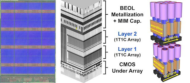
The images above show the final die layout (left) and SEM cross-section (center) of a 32Gb NVDRAM with 1T1C memory layers, fabricated over a CMOS array. On the right is a schematic diagram of NVDRAM memory arrays, showing polysilicon access device with orthogonal wordline (WL) and digitline (DL), and ferroelectric memory cells.

Abstract: Non-Volatile Ferroelectric w/DRAM-Like Performance, for AI & Machine Learning: Rapid growth in the size of the data models used in artificial intelligence (AI) and machine-learning (ML) applications is creating an urgent need for higher-bandwidth memory solutions. While new compute paradigms like near-memory-compute and processing-in-memory are being investigated, the best near-term opportunity is to outfit existing, traditional compute architectures with more efficient memory for faster data movement and to accommodate larger models. In this year’s Generative AI Focus Session, Micron researchers will unveil a memory technology for these uses which they call NVDRAM. It is the world’s first dual-layer, high-performance, high-density (32Gb), stackable and nonvolatile ferroelectric memory technology. It combines the non-volatile, high-endurance nature of ferroelectric memory cells with DRAM-like read/write speeds and endurance, and also surpasses the retention performance of NAND memory. NVDRAM uses an ultra-scaled (5.7nm) ferroelectric capacitor as the memory cell, and a dual-gated, stackable, polycrystalline silicon transistor as the access device. To achieve high memory density, two memory layers are fabricated above CMOS circuitry in a 48nm pitch, 4F2 architecture. Full package yield is demonstrated from -40°C to 95°C, along with reliability of 10 years (for both endurance and retention).

Sources:

Tuesday, September 5, 2023

"Micron to Produce Advanced Memory Chips in Taiwan Using EUV Lithography by 2025, Reinforces Commitment to Island's Semiconductor Industry"

Micron Technology is set to begin producing memory chips in Taiwan using advanced EUV lithography technology by 2025, ahead of its other production sites. The company's local division head, Donghui Lu, confirmed this move and emphasized that Taiwan remains a top investment destination for Micron. The collaboration with Japanese and Taiwanese companies facilitated the development of this technology. 

Micron's decision to produce HBM type memory in Taiwan highlights the island's significance in its operations, accounting for up to 65% of production volumes. The advantageous Taiwanese infrastructure and the company's commitment to geographic diversification contribute to its expanding and modernizing operations. This move underscores Micron's dedication to innovation and maintaining a competitive edge in the semiconductor industry.

Source: Aroged: Micron will begin producing memory in Taiwan using EUV lithography by 2025 - Aroged


Tuesday, February 8, 2022

Samsung Electronics Is Pushing Hard to Bring Monolithic 3D DRAM to HVM by 2025

Samsung Electronics has been enjoying its DRAM market leader position for about 30 years now. To retain the position further, it has intensified its R&D of monolithic 3D DRAMs to bring them to HVM by 2025.


DRAM’s performance boost based on scaling the cell size or pitch is approaching a physical limit for cramming more cells in a limited space. Additionally, the ultra-high aspect ratio capacitors may collapse leading to compromised device reliability. Therefore, switching from current 2D DRAMs to next-generation monolithic 3D DRAMs seems inevitable.

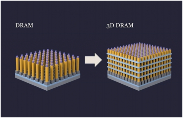
Samsung has reportedly intensified its R&D on stacking DRAM cells on top of each other in a monolithic fashion, unlike in the case of high-bandwidth memory (HBM), wherein multiple dies are stacked atop each other.

Besides High-k/Metal Gate transistor technology, Samsung is also considering adopting FinFET or gate-all-around (GAA) technology for the DRAM cell transistor to attain better electrostatic control of the charge flow within the channel with the gate electrode.

Micron Technology and SK Hynix are also reportedly developing monolithic 3D DRAMs. Micron recently filed a patent for a monolithic 3D DRAM that is different from that of Samsung. Micron’s approach is to change the shapes of the transistor and capacitor without laying down a cell. Major equipment manufacturers such as Applied Materials and Lam Research are also developing solutions for the monolithic 3D DRAMs.

By Abhishek Kumar Thakur & Jonas Sundqvist

Thursday, January 28, 2021

Micron Delivers Industry’s First 1α DRAM Technology

Micron recently announced that they are shipping memory chips built using the world’s most advanced DRAM process technology, which offers major improvements in bit density, power and performance. This is an astonishing feat of nanofabrication. 

Micron announcement: Micron Delivers Industry’s First 1α DRAM Technology

Micron’s 1α DRAM node will facilitate more power-efficient, reliable memory solutions and provide faster LPDDR5 operating speeds for mobile platforms that require best-in-class LPDRAM performance. Micron’s innovation brings the industry’s lowest-power mobile DRAM, with a 15% improvement in power savings,1 allowing 5G mobile users to perform more tasks on their smartphones without sacrificing battery life.

To find out more watch Thy Tran, vice president of DRAM Process Integration at Micron previously with Qimonda explain how to realize this amazing technology.


According to more details given in a Blog by Thy Tran, Micron uses Quadruple Patterning or Quad Patterning to realize the most critical lithography layers, which employ multiple ALD process steps and has become one of the biggest ALD market segment over recent years. See the video below by Lam Research for some more insights!


Quad patterning process flow (Image: Lam Research)


Wednesday, September 2, 2020

TechInsights’ Memory Process: 3D NAND Word Line Pad webinar

TechInsights’ ‘Memory Process: 3D NAND Word Line Pad‘ #webinar compares 9x-layer 3D NAND devices from major manufacturers and discusses the process sequence with emphasis on the word line pad (WLP). Watch on demand here LINK 

Screendump from Webinar

Saturday, November 2, 2019

Micron claim DRAM Technology Leadership As Samsung And SK Hynix Push Out EUV

  • ASML reported that four EUV lithography systems will be pushed out from shipping in 4Q 2019.
  • My analysis suggests Samsung Electronics and SK Hynix are two of the companies pushing our EUV for their memory business.
  • Micron's 1z nm DRAM already is technologically advanced, and are two quarters ahead of Samsung and one year ahead of SK Hynix.

Full article: Micron: DRAM Technology Leadership As Samsung And SK Hynix Push Out EUV, Seeking Alpha (LINK)


A DRAM roadmap by the Information Network showing Micron’s transition to 1z nm and gain of leadership over rivals Samsung and SK Hynix.

Thursday, August 22, 2019

Micron has started volume production of 10 nm-class DRAM (1z nm)

Micron announced on Thursday that it had started volume production of memory chips using its 3rd Generation 10 nm-class fabrication technology (also known as 1Z nm). The first DRAMs to be made using Micron’s 1Z nm process are 16 Gb monolithic DDR4 and LPDDR4X devices. 
The company claims that its 16 Gb DDR4 device consumes 40% less power than two 8 Gb DDR4 DRAMs (presumably at the same clocks). Meanwhile, Micron’s 16 Gb LPDDR4X ICs will bring an up to 10% power saving. One of the first products to use the company’s 16 Gb DDR4 devices will be high-capacity (e.g., 32 GB and higher) memory modules for desktops, notebooks, and workstations.
Source: Anandtech LINK
----------
By Abhishekkumar Thakur

Thursday, January 3, 2019

Innovation and IP filing in Atomic Layer Deposition has moved from Memory to Logic

By studying the filing of IP world wide one can clearly see the trend how innovation in Atomic Layer Deposition (ALD) has moved from Memory to Logic. During the introduction of ALD (2003 to 2006) in high volume manufacturing of DRAM on 300 mm wafers most IP was filed by Samsung, Micron and SK Hynix. 10 years later (2013-2018) the IP filing lead has been taken over by Logic MPU manufacturers TSMC, Intel and Globalfoundries.

The patent application assignee from the past 25 years.