Showing posts with label samsung. Show all posts

Friday, December 29, 2023

Samsung Electronics faces challenges in securing tax breaks from the U.S. government for its new chip plant in Taylor, Texas

Samsung Electronics faces challenges in securing tax breaks from the U.S. government for its new chip plant in Taylor, Texas. Amid stiff competition from Intel, Micron Technology, and over 400 other chipmakers, Samsung's negotiations for subsidies under the $53 billion Chips and Science Act are ongoing. The plant, which will produce AI processors, has delayed its mass production start to 2025 due to rising construction costs and disappointing tax benefits. Intel, Micron, and TSMC are also investing heavily in U.S. facilities, intensifying the competition for government funding. Samsung, while not commenting on the negotiations, has highlighted its substantial U.S. investments and cooperation history at a recent event with U.S. lawmakers.

Friday, December 8, 2023

IBM and Samsung Revolutionize Semiconductor Industry with Groundbreaking VTFET Transistor Technology

In a breakthrough development, IBM and Samsung have introduced a new transistor architecture named Vertical-Transport Nanosheet Field-Effect Transistors (VTFETs), potentially outperforming traditional FinFETs. This exciting innovation was discussed in the AAC Exclusive article, "A Chat With IBM Researchers Who Built the New 'VTFET' Transistor," featuring insights from IBM researchers Brent Anderson and Hemanth Jagannathan.


Comparison of a VTFET (left) vs. a lateral FET (right) transistor with current flowing through them. FinFETs have a limited gate pitch, scaled down to ~48nm, while VTFETs offer more scaling potential with a longer gate length due to their vertical design.

VTFETs offer significant improvements in performance and area scaling, potentially reducing energy usage in devices by up to 85% compared to FinFETs. These transistors operate with a vertical orientation, allowing for longer gates and thicker spacers and source-drains, which reduce resistance and capacitance. This design enables smaller transistor size while enhancing performance.

Anderson and Jagannathan's roles at IBM have been pivotal in the development of VTFETs. Anderson, who joined IBM in 1991, has been instrumental in driving the technology design for various logic nodes, including VTFET. Jagannathan, with IBM for 15 years, has managed process technology groups and played a crucial role in hardware research for VTFET.

Their work signifies a significant step forward in semiconductor technology, promising higher density, performance, and energy efficiency. This innovation represents a potential future for Moore's law scaling, alongside other advancements like monolithic 3D and chip stacking technologies. The real-world implementation of VTFETs is eagerly anticipated, with the technology expected to mature in the coming years.


Wednesday, November 1, 2023

Surge in HBM Demand Marks Memory Market Recovery and Anticipated Growth in 2024 for Samsung

The global memory market, after experiencing a period of stagnation, has witnessed a resurgence in the third quarter, driven primarily by increased demand for high-density DRAM and NAND products in the PC and mobile sectors.

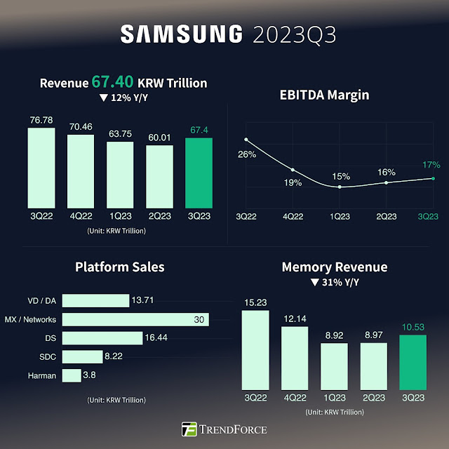
Samsung Electronics' financial results for 3Q23 highlighted a 12% QoQ revenue increase to 67.40 trillion Korean won, although there was a 12% YoY decrease. Notably, the company reported its highest quarterly profit for the year. Despite potential economic uncertainties in 2024, Samsung is optimistic about the recovery of the memory market and the rebound in smartphone demand. 

The memory sector saw a recovery compared to the previous quarter, especially in PC and mobile due to the rise in adoption of high-density DRAM and NAND products. The completion of customer inventory adjustments also played a role. Server demand was subdued for traditional servers due to macroeconomic uncertainties. However, strong demand persisted for AI-oriented high-density products. Samsung emphasized its focus on expanding sales of advanced node products like HBM DDR5, LPDDR5, and UFS 4.0. They also intend to manage high inventory products through production adjustments. The company expects the recovery trend in the memory market to accelerate further in the fourth quarter. Additionally, there has been a notable surge in HBM demand and the company is actively advancing its HBM businesses and plans to augment its HBM supply capacity by 2.5 times next year.


Trendforce on X (LINK)

The foundry division secured a record number of new orders, particularly in the HPC domain, despite a slow recovery in the mobile market. The new Taylor factory in Texas is set to begin production using the second-gen 3nm GAA process. The advanced packaging business has also been flourishing with orders from both domestic and international HPC clients.

Profits in the mobile panel business surged due to new flagship models from major clients. In contrast, the large panel business faced tepid demand. Samsung aims to cater to the growing mobile panel demand and increase profitability in the large panel sector by introducing new products and enhancing yield rates.

With the global economy expected to bounce back in 2024, the smartphone market's demand is anticipated to surge. High-end market growth is likely to continue, driven by the global recovery of the smartphone market.

Looking ahead to 2024, Samsung anticipates increased PC and mobile demand due to product replacement cycles initiated during the pandemic's early phase. High-density trends in both DRAM and NAND are expected to persist, propelled by on-device AI advancements. The company plans to focus on advanced node products, including 1B nanometer DDR5, LPDR5X, PCI Gen 5, and UFS 4.0, to bolster product competitiveness and profitability. Emphasizing the growing demand for generative AI, Samsung aims to strengthen its market position with high-density, low-power, and high-performance products for on-device AI, which has recently gained significant attention.

Sources;

TrendForce on X: "Samsung Electronics has released its financial results for 3Q23, reporting a quarterly revenue of 67.40 trillion Korean won—a 12% QoQ increase but 12% YoY decrease. The company achieved its highest quarterly profit of the year and anticipates that, despite ongoing global economic… https://t.co/RDKVjimgzN" / X (twitter.com)

Samsung Electronics Co Ltd (SSNLF) Q3 2023 Earnings Conference Call Transcript | Seeking Alpha


Tuesday, May 2, 2023

TechInsights found Samsung DRAM chips in Samsung Galaxy S23 with Five EUV mask layers

TechInsights found Samsung DRAM chips in Samsung Galaxy S23 with Five EUV mask layers. These are from DRAM wafers produced in the so-called D1a node (or D1α, α as in alpha)


This is in line with a previous press release from Samsung (2020) so no real surprise here: Samsung Announces Industry’s First EUV DRAM with Shipment of First Million Modules – Samsung Global Newsroom

"EUV to be fully deployed from 4th-gen 10nm-class DRAM (D1a) next year"

EUV will be fully deployed in Samsung’s future generations of DRAM, starting with its fourth-generation 10nm-class (D1a) or the highly-advanced 14nm-class, DRAM. Samsung expects to begin volume production of D1a-based DDR5 and LPDDR5 next year, which would double manufacturing productivity of the 12-inch D1x wafers.


Friday, November 4, 2022

Samsung use NCD ALD for wirebonding alternatives to expensive Gold

According to a recent article by TheElec, Samsung has developed a new chip packaging technology with its key partners for automotive chips. The company employs an aluminum oxide (Al2O3) coating bonding wire technology with improved reliability and insulation compared to previous bonding wires.

Bonding wires connect the I/Os with the lead frame or printed circuit boards. Most of them in the past have been made with gold (Au) as they are flexible and conductive. But as gold prices continue to rise, many companies attempt to mix them with silver (Ag) or copper (Cu). However,  these mixed materials usually have weak adhesiveness with their coating materials. This is unacceptable for chips aimed at automobiles as they are exposed to high-temperature and high-humidity environments.

Samsung’s aluminum alternative, which it is developing with Electron, NCD and LT Metal, doesn’t have this weakness since the aluminum oxide is coated at nanometer thinness onto the metal used as wire. Aluminum oxide bonds well with insulating coating materials that use epoxy. The precursors used to coat the aluminum oxide such as tri-metal aluminum (TMA) are also relatively cheap and used in HVM since a long time.


Insulated, Passivated & Adhesively-Promoted Bond WireUsing All-in-One Al2O3 Coating

Soojae Park(1), Jonghyun Lee(1), Chulhyung Cho(1), Namhoon Kim(1), Yongje Lee(1), Sichun Seo(1), Manho Kim(1), Youngkwon Yoon(1), EulgiMin(2), Kyujung Choi(2), Sang-Hoon Lee(3) Hong-Sik Nam(3),Monghyun Cho(4) & Jeongtak Moon(4),(1)Samsung Electronics Company130 Samsung-Ro, Yungtong-Gu, Suwon-Si, Gyunggi-Do, Republic of Korea(2)NCD Co., Ltd.(3)LT Metal, Ltd.(4)MK Electron Co., Ltd. (2) (PDF) Insulated, Passivated & Adhesively-Promoted Bond Wire Using All-in-One Al2O3 Coating. Available from:

Sunday, September 18, 2022

Samsung to focus on treatment of gas used in chip production to achieve net-zero emissions

A major cause of greenhouse gas emissions is process gas used in semiconductor wafer manufacturing comes from processing equipment such as reactive ion etching (RIE) and deposition (CVD and ALD). You can read and watch an interview here and study that paper that was recently published by me and my professor friends Henrik Pedersen and Sean Barry:


Green CVD-Toward a sustainable philosophy for thin film deposition by chemical vapor deposition

It is almost obvious that higher VPs at Samsung and TSMC (LINK) did just that ;-)

[Korea Herald, Link below] Advancing abatement technologies to reduce carbon emissions is the top priority in the Samsung Electronics semiconductor unit's goal to become carbon neutral by 2050, a top official said Friday.

"Treatment of gas used to manufacture semiconductor chips is our biggest focus in our spending (to achieve net-zero emissions)," Song Doo-guen, executive vice president and head of the Environment & Safety Center at Samsung Electronics, told reporters at a briefing in Seoul.


According to the article, Song Doo-guen, executive vice president and head of the Environment & Safety Center at Samsung Electronics, speaks at a briefing in Seoul, Friday and announced that:
  • Samsung has pledged a 7 trillion won ($5 billion) investment to achieve its climate ambitions, and announced that it had recently joined RE100, a coalition comprising 380 global enterprises committed to becoming 100 percent renewable.
  • Alongside the plan to cut direct carbon emissions, Samsung has also laid out a raft of plans to reduce indirect emissions, mainly by pursuing ultralow-power chip products.
  • Other eco-conscious plans it has drawn up include capping the maximum use of freshwater to 300,000 tons a day by 2030 and eradicating gaseous and liquid pollutants by 2040 with treatment technology.
Source: Samsung chip plants look to stamp out carbon footprint (koreaherald.com)

Sunday, September 4, 2022

Samsung Electronics Breaks Ground on New Semiconductor R&D Complex in Giheung, Korea

Samsung to invest KRW 20 trillion by 2028 to build advanced research facility

Samsung Electronics recently broke ground for a new semiconductor research and development complex in Giheung, Korea, aiming to extend its leadership in state-of-the-art semiconductor technology.

  • Samsung Electronics plans to invest about KRW 20 trillion by 2028 for the complex in an area covering about 109,000 square meters within its Giheung campus. 
  • The new facility will lead advanced research on next-generation devices and processes for memory and system semiconductors, as well as development of innovative new technologies based on a long-term roadmap.


Today’s groundbreaking ceremony was attended by Samsung Electronics Vice Chairman Jay Y. Lee, President and CEO Kye Hyun Kyung, President of the Memory Business Jung-Bae Lee, President of the Foundry Business Siyoung Choi and President of the S.LSI Business Yong-In Park, along with more than 100 employees.

“Our new state-of-the-art R&D complex will become a hub for innovation where the best research talent from around the world can come and grow together,” said President Kye Hyun Kyung, who also heads the Device Solutions (DS) Division. “We expect this new beginning will lay the foundation for sustainable growth of our semiconductor business.”


Samsung Electronics’ Giheung campus, located south of Seoul near the DS Division’s Hwaseong campus, is the birthplace of the world’s first 64Mb DRAM in 1992, marking the beginning of the company’s semiconductor leadership.

Wednesday, June 22, 2022

NCD supplied ALE and ASD equipment to Samsung Electronics Co., Ltd.

NCD has recently supplied ASD (Area Selective Deposition) equipment to Samsung Electronics Co., Ltd. Following ALE (Atomic Layer Etching).

This is the cluster system which consists of two process modules (PMs) and a wafer transfer module (TM) and applies a running program for process integration. In addition, it is equipped to process at high temperatures up to 500℃ and process with ozone and plasma for developing the next semiconductor devices.

ALE is able to etch a deposited layer by atomic scale as opposed to ALD and ASD can only deposit on the selective area not grow the whole area of substrates by ALD.

Today, lots of universities, institutes, and companies have actively been developing future high-tech and highly integrated devices using ALE and ASD processes.

NCD expects that the ALE/ASD system will contribute very much to the development of high-end semiconductor technology and is going to do all of the efforts to the best ALD equipment company with new challenges and continuous R&D.

<Lucida M200PL Series ALD System>


Tuesday, February 8, 2022

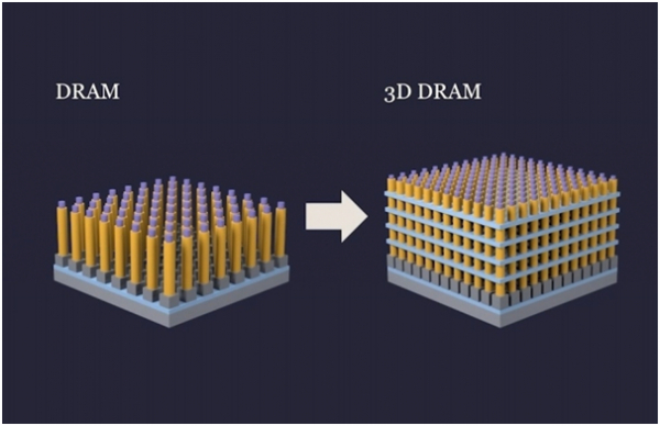
Samsung Electronics Is Pushing Hard to Bring Monolithic 3D DRAM to HVM by 2025

Samsung Electronics has been enjoying its DRAM market leader position for about 30 years now. To retain the position further, it has intensified its R&D of monolithic 3D DRAMs to bring them to HVM by 2025.


DRAM’s performance boost based on scaling the cell size or pitch is approaching a physical limit for cramming more cells in a limited space. Additionally, the ultra-high aspect ratio capacitors may collapse leading to compromised device reliability. Therefore, switching from current 2D DRAMs to next-generation monolithic 3D DRAMs seems inevitable.

Samsung has reportedly intensified its R&D on stacking DRAM cells on top of each other in a monolithic fashion, unlike in the case of high-bandwidth memory (HBM), wherein multiple dies are stacked atop each other.

Besides High-k/Metal Gate transistor technology, Samsung is also considering adopting FinFET or gate-all-around (GAA) technology for the DRAM cell transistor to attain better electrostatic control of the charge flow within the channel with the gate electrode.

Micron Technology and SK Hynix are also reportedly developing monolithic 3D DRAMs. Micron recently filed a patent for a monolithic 3D DRAM that is different from that of Samsung. Micron’s approach is to change the shapes of the transistor and capacitor without laying down a cell. Major equipment manufacturers such as Applied Materials and Lam Research are also developing solutions for the monolithic 3D DRAMs.

By Abhishek Kumar Thakur & Jonas Sundqvist

Tuesday, June 1, 2021

South Korean equipment makers recorded mixed results in the first quarter of 2021

출처 : THE ELEC, Korea Electronics Industry Media(http://thelec.net) - South Korean equipment makers recorded mixed results in the first quarter of 2021.

  • Fab equipment vendors posted high growth, while display equipment firms underperformed.
  • Fab equipment makers benefited from aggressive spending by semiconductor companies.
  • CVD/ALD equipment companies showed good growth, see below (Jusung, Wonik IPD, Eugene Technologies

Semes, Samsung Electronics’ fab equipment subsidiary, recorded 870.6 billion won in sales, an increase of 62.3% from a year prior. It recorded 112.8 billion won in operating income, an increase of 40.5% over the same time period. The growth likely stems from Samsung starting to put in equipment to its P2 chip line at its Pyeontaek plant during the quarter. Overheat transport accounted for 60% of the sales recorded by Semes during the quarter.

SFA recorded 355.6 billion won in sales and 42.3 billion won in operating income, a drop of 3.3% and 1.6%, respectively, a year prior. Non-display business accounted for 65.1% of its sales. SFA, which previously focused on display kits, managed to record level earnings to a year prior thanks to other business areas.


Wonik IPS recorded 254.5 billion won in revenue and 24.2 billion won in operating income, a surge of 39.9% and 68.1%, respectively, from a year prior. The firm previously focused on fab equipment for use in memory chip production. But it has begun supplying kits for foundry beginning last year, which helped growth.

Eugene Technology recorded 100.7 billion won in revenue and 30.7 billion won in operating income. The company recorded an operating margin rate of 30.5%. Its LPCVD equipment supplied to SK Hynix for the latter’s M16 DRAM fab led the growth.

Jusung Engineering posted 75.3 billion won in sales in the quarter, double that of the year prior. It turned a profit from a year prior and posted 16 billion won in operating income. The company won the order for atomic layer deposition kits from SK Hynix for use in next-generation DRAMs. Jusung is the sole supplier of the kits.

Hanmi Semiconductor recorded 70.9 billion won in sales, a jump of 79% from a year prior. Its operating income increased 160% year-on-year to 19.3 billion won. It won 22 orders during the quarter. It has signed supply deals with SK Hynix, Amkor Technology Korea, ASE, NXP, Nanya, SPIL and others for a combined worth of 87 billion won.

YIK recorded 67.5 billion won in sales and 9.7 billion won in operating income, a jump of 99.7% and 177.1%, respectively, from a year prior. The firm mainly provides electrical die sorting equipment. The firm is seeing more orders from Samsung, having signed a 155.3 billion won deal with the tech giant in the first quarter alone.

South Korean fab equipment makers are expected to post solid growth throughout 2021 from increased spending this year by Samsung and SK Hynix. SK Hynix had said in the conference call for the first quarter that it plans to execute some of its spending it planned for 2022 earlier to this year.

SEMI is expecting global fab equipment spending to increase 15.5% this year to US$70 billion. Meanwhile, South Korean display equipment makers underperformed during the first quarter.

Samsung Display and LG Display have been conservative with their spending due to uncertainties surrounding the display market. But increased spending in OLED from Chinese panel makers such as BOE and Tianma staved off a huge dip in profitability.

Only few companies recorded growth, such as AP Systems, which saw sales drop 6.9% year-on-year but operating income surge 53.2% over the same time period. The company benefited from laser annealing equipment supplied to BOE for the B12 line.

Youngwoo DSP saw a surge in its operating income from supplies to its Chinese customers. KC Tech saw sales jump 21.1% but operating income remained flat. Top Engineering saw 9.6 billion won in operating loss from the 6.1 billion won operating loss posted by subsidiary Powerlogics. Dong A Eltek recorded 2.3 billion won in operating loss, though sales doubled. The firm said increased cost from the pandemic stunted growth.

Charm Engineering continued to record loss. HB Technology, Toptec and Philoptics all turned to the red. 

Local display equipment makers are expected to see a turnaround starting in the fourth quarter when Samsung Display and LG Display decide on new spending plans around the same time.


Friday, March 26, 2021

Samsung confirms first HKMG for DDR5 DRAM

ASM International recently acknowledged that ALD High-k/Metal Gate (HKMG) is finally in high volume production for DRAM (LINK). Now Samsung confirms that. This is a small victory for all people working on this process for such a long time. My first tool ownership when I moved to Germany and started at Infineon was an ASM Polygon 200 mm cluster with a Pulsar 2000 chamber running HfO2, TiN, TiHfN, TiAlN, Al2O3, and my not fully understood HfN ALD process and a Poly chamber that I never really cared too much about. Press release below - and now do the maths - how big this business is once rolled out for all DRAM technologies to come - yeah $$$, many tulips indeed.


Samsung Develops Industry’s First HKMG-Based DDR5 Memory; Ideal for Bandwidth-Intensive Advanced Computing Applications

512GB capacity DDR5 module made possible by an 8-layer TSV structure
HKMG material reduces power by 13 percent while doubling the speed of DDR4


Samsung Electronics, the world leader in advanced memory technology, today announced that it has expanded its DDR5 DRAM memory portfolio with the industry’s first 512GB DDR5 module based on High-K Metal Gate (HKMG) process technology. Delivering more than twice the performance of DDR4 at up to 7,200 megabits per second (Mbps), the new DDR5 will be capable of orchestrating the most extreme compute-hungry, high-bandwidth workloads in supercomputing, artificial intelligence (AI) and machine learning (ML), as well as data analytics applications.


“Samsung is the only semiconductor company with logic and memory capabilities and the expertise to incorporate HKMG cutting-edge logic technology into memory product development,” said Young-Soo Sohn, Vice President of the DRAM Memory Planning/Enabling Group at Samsung Electronics. “By bringing this type of process innovation to DRAM manufacturing, we are able to offer our customers high-performance, yet energy-efficient memory solutions to power the computers needed for medical research, financial markets, autonomous driving, smart cities and beyond.”

“As the amount of data to be moved, stored and processed increases exponentially, the transition to DDR5 comes at a critical inflection point for cloud datacenters, networks and edge deployments,” said Carolyn Duran, Vice President and GM of Memory and IO Technology at Intel. “Intel’s engineering teams closely partner with memory leaders like Samsung to deliver fast, power-efficient DDR5 memory that is performance-optimized and compatible with our upcoming Intel Xeon Scalable processors, code-named Sapphire Rapids.”

Samsung’s DDR5 will utilize highly advanced HKMG technology that has been traditionally used in logic semiconductors. With continued scaling down of DRAM structures, the insulation layer has thinned, leading to a higher leakage current. By replacing the insulator with HKMG material, Samsung’s DDR5 will be able to reduce the leakage and reach new heights in performance. This new memory will also use approximately 13% less power, making it especially suitable for datacenters where energy efficiency is becoming increasingly critical.

The HKMG process was adopted in Samsung’s GDDR6 memory in 2018 for the first time in the industry. By expanding its use in DDR5, Samsung is further solidifying its leadership in next-generation DRAM technology.

Leveraging through-silicon via (TSV) technology, Samsung’s DDR5 stacks eight layers of 16Gb DRAM chips to offer the largest capacity of 512GB. TSV was first utilized in DRAM in 2014 when Samsung introduced server modules with capacities up to 256GB.

Samsung is currently sampling different variations of its DDR5 memory product family to customers for verification and, ultimately, certification with their leading-edge products to accelerate AI/ML, exascale computing, analytics, networking, and other data-intensive workloads


Friday, February 26, 2021

Tech Insights Teardown: Samsung’s D1z DRAM with EUV Lithography

Advanced and costly schemes for ArFi immersion-based multi-pattering are definitely running out of steam for leading-edge logic and EUV is continuing the march into high volume manufacturing now also for DRAM. The other day there was an announcement that SK Hynix, the world´s number two DRAM maker has signed a 5-year agreement with ASML for EUV scanners (LINK).

As a European, I must say that I like the situation that the key to continued scaling is kept in The Netherlands (ASML) and also the important key technology providers in Germany (Zeiss SMT, Trumpf) and Belgium in the form of the worlds leading research institute for scaling CMOS - imec and the EUV Resist Manufacturing & Qualification Center NV (EUV RMQC), a Joint Venture between imec and  JSR Micro NV (LINK).

Reuters: SK Hynix signs five-year deal worth $4.3 billion with ASML to secure EUV scanners


Now DRAMs from Samsung Electronics with applied EUV lithography technology for D1z DRAM in mass production have been found in the field and analyzed by Tech Insights and reported by EETimes (LINK).

According to EETimes, Samsung Electronics announced the world’s first development of both ArF-i based D1z DRAM and separately its EUV lithography (EUVL) applied D1z DRAM last year.

Tech Insights is excited that we have finally found Samsung’s new and advanced D1z DRAM devices and confirmed details of this technology.

Here just a teaser, please check out the original EETimes article or get the full report from Tech Insights (LINK).


Samsung DRAM cell design, a comparison of BLP patterns on D1z (a) without EUVL and (b) with EUVL.


Saturday, November 28, 2020

Intel remains in the lead in 2020 semiconductor sales

IC Insights’ November shows the forecasted top-25 semiconductor suppliers in 2020. Seven top-15 semiconductor suppliers forecast to show ≥22% growth this year with Nvidia expected to post a huge 50% increase. The top-15 companies semiconductor sales are broken out into IC and O-S-D (optoelectronic, sensor, and discrete) device categories for 2019 and 2020. The forecasted 2020 top-15 semiconductor supplier ranking includes eight suppliers headquartered in the U.S., two each in South Korea, Taiwan, and Europe, and one in Japan.

Intel remains No 1. followed by Samsung and TSMC. 2020 show a very high growth for Fabless companies Qualcomm, Nvidia, MediaTek, Apple and AMD.

The Memory segment (DRAM and Flash) is led by SK Hynix +14% followed by Samsung +9% (incl. foundry) and Micron is down by -3%.

Please read the full IC Insights report here: LINK


Wednesday, October 28, 2020

Stanford and Samsung Display use solar panel tech to create new ultrahigh-res OLED display

Stanford University reports that by expanding on existing designs for electrodes of ultra-thin solar panels, Stanford researchers and collaborators in Korea have developed a new architecture for OLED – organic light-emitting diode – displays that could enable televisions, smartphones and virtual or augmented reality devices with resolutions of up to 10,000 pixels per inch (PPI). (For comparison, the resolutions of new smartphones are around 400 to 500 PPI.) 

The crucial innovation behind both the solar panel and the new OLED is a base layer of reflective metal with nanoscale (smaller than microscopic) corrugations, called an optical metasurface. The metasurface can manipulate the reflective properties of light and thereby allow the different colors to resonate in the pixels. These resonances are key to facilitating effective light extraction from the OLEDs. 


Illustration of the meta-OLED display and the underlying metaphotonic layer, which improves the overall brightness and color of the display while keeping it thin and energy efficient. (Image credit: Courtesy Samsung Advanced Institute of Technology) 

In lab tests, the researchers successfully produced miniature proof-of-concept pixels. Compared with color-filtered white-OLEDs (which are used in OLED televisions) these pixels had a higher color purity and a twofold increase in luminescence efficiency – a measure of how bright the screen is compared to how much energy it uses. They also allow for an ultrahigh pixel density of 10,000 pixels-per-inch.

Full Report: Stanford materials scientists borrow solar panel tech to create new ultrahigh-res OLED display LINK

Wednesday, September 2, 2020

TechInsights’ Memory Process: 3D NAND Word Line Pad webinar

TechInsights’ ‘Memory Process: 3D NAND Word Line Pad‘ #webinar compares 9x-layer 3D NAND devices from major manufacturers and discusses the process sequence with emphasis on the word line pad (WLP). Watch on demand here LINK 

Screendump from Webinar

Wednesday, July 8, 2020

Samsung Leads Semiconductor Paradigm Shift with New Material Discovery : Amorphous Boron Nitride as Ultra Low-k

[Samsung Newsroom, LINK] Researchers at the Samsung Advanced Institute of Technology (SAIT) have unveiled the discovery of a new material, called amorphous boron nitride (a-BN), in collaboration with Ulsan National Institute of Science and Technology (UNIST) and the University of Cambridge. Published in the journal Nature, the study has the potential to accelerate the advent of the next generation of semiconductors.

2D Materials – The Key to Overcoming Scalability Challenges

Recently, SAIT has been working on the research and development of two-dimensional (2D) materials – crystalline materials with a single layer of atoms. Specifically, the institute has been working on the research and development of graphene, and has achieved groundbreaking research outcomes in this area such as the development of a new graphene transistor as well as a novel method of producing large-area, single-crystal wafer-scale graphene. In addition to researching and developing graphene, SAIT has been working to accelerate the material’s commercialization.

“To enhance the compatibility of graphene with silicon-based semiconductor processes, wafer-scale graphene growth on semiconductor substrates should be implemented at a temperature lower than 400°C.” said Hyeon-Jin Shin, a graphene project leader and Principal Researcher at SAIT. “We are also continuously working to expand the applications of graphene beyond semiconductors.”

Cross-sectional imaging reveals that amorphous boron nitride prevents the diffusion of cobalt atoms into silicon under very harsh conditions, in contrast to reference barriers. Our results demonstrate that amorphous boron nitride has excellent low-κ dielectric characteristics for high-performance electronics. (From Nature Publication,  LINK)

Amorphous boron nitride has a best-in-class ultra-low dielectric constant of 1.78 with strong electrical and mechanical properties, and can be used as an interconnect isolation material to minimize electrical interference. (Graphics: Samsung)

2D Material Transformed – Amorphous Boron Nitride

The newly discovered material, called amorphous boron nitride (a-BN), consists of boron and nitrogen atoms with an amorphous molecule structure. While amorphous boron nitride is derived from white graphene, which includes boron and nitrogen atoms arranged in a hexagonal structure, the molecular structure of a-BN in fact makes it uniquely distinctive from white graphene.

Amorphous boron nitride has a best-in-class ultra-low dielectric constant of 1.78 with strong electrical and mechanical properties, and can be used as an interconnect isolation material to minimize electrical interference. It was also demonstrated that the material can be grown on a wafer scale at a low temperature of just 400°C. Thus, amorphous boron nitride is expected to be widely applied to semiconductors such as DRAM and NAND solutions, and especially in next generation memory solutions for large-scale servers.

“Recently, interest in 2D materials and the new materials derived from them has been increasing. However, there are still many challenges in applying the materials to existing semiconductor processes.” said Seongjun Park, Vice President and Head of Inorganic Material Lab, SAIT. “We will continue to develop new materials to lead the semiconductor paradigm shift.”

Publication:

Ultralow-dielectric-constant amorphous boron nitride, Nature volume 582pages511514(2020) LINK

Thursday, May 21, 2020

Reuters: Samsung Electronics builds sixth domestic contract chip-making line

Samsung breaks the ground for building its 6th domestic production line in Pyeongtaek city to expand its 5 nm chip-production capacity, using EUV technology: Samsung has planned to expand its production of logic chips for mobile phones and computers as it looks to cut reliance on the volatile memory chip sector. The new production line is targeted to be operational by 2H21. Last year, Samsung announced to invest 133 trillion won ($107.97 billion) in non-memory chips through 2030, comprising 73 trillion won for domestic R&D and 60 trillion won for production infrastructure.

Source: Reuters LINK

----------
By Abhishekkumar Thakur

Saturday, January 4, 2020

Samsung's 3 nm Gate-All-Around FET prototype

Samsung has succeeded in making the first strides towards the 3 nm process, as reported by the Korean Maeil Economy this week. According to the report, Samsung's goal is to become the world's number one semiconductor manufacturer by 2030.

Samsung's work on the 3 nm process is based on the Gate All Around (GAAFET) technology rather than FinFET. This supposedly reduces the total silicon size by 35% while using about 50% less power and allows for the same amount of power consumption and 33% performance increase over the 5 nm FinFET process.


Gate-All-Around FETs - Picture credit: Samsung

Source: Toms Hardware (LINK)

----------
By AbhishekkumarThakur

Saturday, November 2, 2019

Micron claim DRAM Technology Leadership As Samsung And SK Hynix Push Out EUV

  • ASML reported that four EUV lithography systems will be pushed out from shipping in 4Q 2019.
  • My analysis suggests Samsung Electronics and SK Hynix are two of the companies pushing our EUV for their memory business.
  • Micron's 1z nm DRAM already is technologically advanced, and are two quarters ahead of Samsung and one year ahead of SK Hynix.

Full article: Micron: DRAM Technology Leadership As Samsung And SK Hynix Push Out EUV, Seeking Alpha (LINK)


A DRAM roadmap by the Information Network showing Micron’s transition to 1z nm and gain of leadership over rivals Samsung and SK Hynix.

Friday, March 15, 2019

Samsung’s GAA Transistor, MBCFET™ aims at Reduced Size and Increased Performance

While chipmakers are struggling with the FinFET based chip production below 5 nm process nodes, Samsung has planned to opt for GAA (gate all around) architecture. Samsung’s GAA redesigns the transistor, making it more power-efficient and better-performing than the existing Multi Bridge Channel FET (MBCFET™) that utilize stacked nanosheets. 
 
Samsung’s patented MBCFET™ is formed as a nanosheet, allowing for a larger current and simpler device integration. It allows to reduce the operating voltage below 0.75 V that had been extremely difficult with FinFET. This yields to 50% less power consumption or 30% more performance at 45% less chip area compared to 7 nm FinFET technology. Also, Samsung's GAA technology is compatible with current FinFET production line that means the today's fab running on mature process tools and methodology can be utilized for GAA transistors. Here is the infographic to learn more about how Samsung’s GAA is advancing the future of semiconductor technology.

Source: Samsung LINK

Written by : Abhishekkumar Thakur and Jonas Sundqvist