Showing posts with label ruthenium. Show all posts

Thursday, June 23, 2022

TANAKA Establishes New Ruthenium Film Deposition Process That Contributes Toward Improved Durability Of Semiconductors

TANAKA Kikinzoku Kogyo K.K. (Head office: Chiyoda-ku, Tokyo; Representative Director & CEO: Koichiro Tanaka), which operates the TANAKA Precious Metals manufacturing business, announced today that TANAKA has established a two-stage film deposition process using the liquid ruthenium (Ru) precursor "TRuST." TRuST is a precursor that has excellent reactivity with both oxygen and hydrogen and can form high-quality ruthenium films. This process is a two-stage atomic layer deposition (ALD) process that uses hydrogen film formation to create a thin anti-oxidation film and oxygen for the deposition of a high-quality ruthenium film. It eradicates concerns that the substrate will become oxidized and, at the same time, can prevent the drop in ruthenium purity that occurs during hydrogen film deposition


The film deposition process was proposed by Professor Soo-Hyun Kim from the School of Materials Science and Engineering, College of Engineering, Yeungnam University in South Korea. The development and evaluation of the film deposition process were jointly conducted by Professor Kim and TANAKA Kikinzoku Kogyo.

This technology is expected to achieve greater miniaturization and improved durability of semiconductors. It can therefore be expected to be used in data centers and smartphones - which require even greater data processing capabilities - and contribute toward advanced technologies such as IoT and autonomous driving, which require sophisticated technological innovations.

Two-Stage Film Deposition Process Using Oxygen And Hydrogen

TANAKA Kikinzoku Kogyo is developing high-purity precious metal precursors centered on ruthenium for next-generation semiconductors. So far, single-stage film deposition using oxygen has been the mainstream process for film deposition. However, the company has now succeeded in a two-stage film deposition process using oxygen and hydrogen.

This two-stage film deposition process reduces the risk of surface oxidation of the base caused by hydrogen film deposition and allows high-purity film deposition that maintains ruthenium purity at almost 100% using oxygen film deposition. Furthermore, by forming the base first using hydrogen film deposition, the ruthenium film on top of the base created using oxygen film deposition will be smooth and dense, achieving a lower resistance than before.

Generally, specific resistivity increases when film thickness decreases, which is an issue in film deposition of semiconductors. With this new process, it was confirmed that an even lower resistance results from a two-stage film deposition that uses hydrogen in addition to oxygen film deposition, especially in the range of 10 nm and below. As semiconductors become even smaller in scale in the future, demand for thinner film deposition with low resistance is also expected for ruthenium films, and a two-stage film deposition allows this issue to be resolved. In addition, the new low-resistance, high-purity ruthenium film created by the two-stage film deposition can be achieved using the same raw materials and film deposition temperature for both stages. Therefore, film deposition is possible using the same film deposition equipment, allowing capital investment costs to be suppressed. Details will be announced at the AA2-TuA: ALD for BEOL session of the ALD 2022 conference being held in Ghent, Belgium, on June 28, 2022.

TANAKA Kikinzoku Kogyo's Liquid Ruthenium Precursor "TRuST"

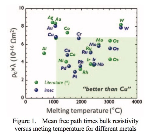
In the past, the most common thin film and wiring materials used for semiconductors were copper, tungsten, and cobalt, but there are increasing expectations for the precious metal ruthenium to promote greater miniaturization of semiconductors because of its lower resistance and higher durability. Therefore, TANAKA Kikinzoku Kogyo developed TRuST - a liquid ruthenium precursor for chemical vapor deposition (CVD) and ALD that achieved the world's highest vapor pressure value - and started providing samples in 2020.

By increasing to the world's highest vapor pressure value, which is more than 100 times higher than existing precursors, this precursor raises the concentration of precursor in the film deposition chamber and the adsorption density of precursor molecules on the substrate surface, achieving excellent step coverage and improved film deposition speed.

State of the Semiconductor Industry and Background

The progress of advanced technologies such as IoT, AI, 5G, and the metaverse has led to rapidly increasing volumes of digital data used by digital devices such as smartphones. Therefore, in the development of semiconductors, the need for even greater miniaturization is increasing to enable the creation of devices with higher performance and lower energy consumption. In the aspect of durability, degradation due to base oxidation is also a major issue in semiconductor development. Furthermore, the development of electric vehicles and self-driving cars requires similar needs for the miniaturization of automotive semiconductors along with further improvement in durability.

In the semiconductor industry, which will require greater miniaturization and improved durability in the future, TANAKA Kikinzoku Kogyo seeks to further reduce costs and achieve higher quality by improving the film deposition speed of liquid ruthenium precursors. At the same time, the company will contribute to greater miniaturization and improved durability of semiconductors to support the development of new advanced technologies enabled by semiconductors.

Thursday, September 30, 2021

Selectivity Enhancement for Ruthenium Atomic Layer Deposition in Sub-50 nm Nanopatterns by Diffusion and Size-Dependent Reactivity

Area-selective deposition (ASD) is a promising bottom-up approach for fabricating nanoelectronic devices. The challenge is to prevent the undesired growth of nanoparticles in the nongrowth area. 

In this work from Belgium and The Netherlands research teams, linewidths of 50 nm and smaller, all Ru adspecies are captured at the growth interface before growth by precursor adsorption is catalyzed. This is more than 1000 times lower than for patterns with a linewidth of 200 nm and larger, where the Ru content decreases significantly only near the interface with the growth surface. 

The predicted depletion zone is confirmed by experiments in nanoscale line-space patterns. Overall, this mechanism results in smaller and fewer Ru nanoparticles for smaller patterns, facilitating the development of passivation-deposition-etch ASD processes for nanoelectronic device fabrication.

Selectivity Enhancement for Ruthenium Atomic Layer Deposition in Sub-50 nm Nanopatterns by Diffusion and Size-Dependent Reactivity

Jan-Willem J. Clerix, Esteban A. Marques, Job Soethoudt, Fabio Grillo, Geoffrey Pourtois, J. Ruud Van Ommen, Annelies Delabie,
3 September 2021


Area-selective deposition (ASD) is a promising bottom-up approach for fabricating nanoelectronic devices. However, a challenge is to prevent the undesired growth of nanoparticles in the nongrowth area. This work uses kinetic Monte Carlo (KMC) methods to investigate the defectivity in ruthenium ASD by (ethylbenzyl)(1-ethyl-1,4-cyclohexadienyl)Ru/O2 (EBECHRu) atomic layer deposition (ALD) in line-space nanopatterns with different dimensions. Ru ASD is governed by adsorption as well as diffusion. The defectivity depends on the pattern dimensions, as nanoparticles can diffuse and reach the interface with the growth area where they aggregate. For linewidths of 50 nm and smaller, all Ru adspecies are captured at the growth interface before growth by precursor adsorption is catalyzed. The synergetic effect of diffusion and size-dependent reactivity reduces defectivity below 1010 Ru atoms cm−2 for at least 1000 ALD cycles. This is more than 1000 times lower than for patterns with a linewidth of 200 nm and larger, where the Ru content decreases significantly only near the interface with the growth surface. The predicted depletion zone is confirmed by experiments in nanoscale line-space patterns. Overall, this mechanism results in smaller and fewer Ru nanoparticles for smaller patterns, facilitating the development of passivation-deposition-etch ASD processes for nanoelectronic device fabrication.


Sunday, February 3, 2019

Low temperature ALD of Rutheium using H2O as co-reactant

For those of you who were not surprised when Helsinki University published their Ru ALD processing using air as co-reactant please behold - Ruthenium ALD using H2O as co-reactant!

Self-catalyzed, Low-temperature Atomic Layer Deposition of Ruthenium Metal Using Zero-valent, Ru(DMBD)(CO)3 and Water
 
Zhengning Gao, Duy Le, Asim Khaniya, Charles L. Dezelah, Jacob Woodruff, Ravindra K. Kanjolia, William E Kaden, Talat S. Rahman, and Parag Banerjee
Chem. Mater., Just Accepted Manuscript
DOI: 10.1021/acs.chemmater.8b04456

Ruthenium (Ru) films are deposited using atomic layer deposition (ALD), promoted by a self-catalytic reaction mechanism. Using zero-valent, η4-2,3-dimethylbutadiene Ruthenium tricarbonyl (Ru(DMBD)(CO)3) and H2O, Ru films are deposited at the rate of 0.1 nm/cycle. The temperature for steady deposition lies between 160 ○C and 210 ○C. Film structure and composition is confirmed via x-ray diffraction, high-resolution transmission electron microscopy and x-ray photoelectron spectroscopy. The room temperature electrical resistivity of 10 nm Ru films is found to be 39 µΩ.cm. In situ quadrupole mass spectrometry and ab initio density functional theory are used to understand ALD surface reactions. The ligand, dimethylbutadiene dissociatively desorbs on the surface. On the other hand, the carbonyl ligand is catalyzed by the Ru center. This leads to the water gas shift reaction, forming CO2 and H2. Modulating deposition temperature affects these two ligand dissociation reactions. This in turn affects nucleation, growth and hence, Ru film properties. Self-catalyzed reactions provide a pathway for low temperature ALD with milder co-reactants.


Tuesday, January 8, 2019

Review form IEDM2018 - The World After Copper

Here is a very good review form IEDM2018 - The World After Copper by Paul McLellan

Thank you for sharing this one Henrik Pedersen! Indeed, Ru is coming!

IEDM: The World After Copper

I remember Gary Patton, the CTO of GLOBALFOUNDRIES, telling me once that research seemed to have flipped, and whereas he used to have most people working on transistors and interconnect was an afterthought, now it was the other way around. Just scaling the existing copper interconnect to get to the next generation was no longer enough.

At IEDM in December, there was a special session called Interconnects to Enable Continued Scaling. There were invited presentations by:
  • Arm and Georgia Tech
  • IBM
  • imec
  • UT Austin and GLOBALFOUNDRIES
  • Stanford
  • Applied Materials
Continue reading LINK 

Wednesday, January 2, 2019

IEDM 2018 Imec on Interconnect Metals Beyond Copper

At IEDM in December 2018 Imec presented recent results from their interconnect program “Interconnect metals beyond copper – reliability challenges and opportunities”, which was recently covered by Scotten Jones (SemiWiki).
 

The electrical current in interconnect lines haven’t scaled down as fast as the lines' cross sectional area, which has enhanced the current density in the lines. Initial wide aluminum (Al) interconnects were first replaced by narrower aluminum-copper (AlCu) alloys and eventually by Cu to reduce the interconnects line resistance. Now even Cu needs to be replaced by alternate materials for the narrowest lines due to the following limits:

  • Higher resistivity with shrinking line width – below 20nm exponential increase in line resistance.
  • Via resistance also goes up strongly due to the liner.
  • Thinner lines see more grains from electroplating – around 10nm line can’t meet electromigration.
Imec commenced their work on alternative materials for M0 and M1 interconnects by screening based on the two metrics—resistivity multiplied by electron mean free path and melting point. The work reflects Rhodium and Iridium as the best candidate materials for the lowest interconnects that can be reasonably integrated. Ruthenium (Ru) and Cobalt (Co) exhibit similar performance. These materials can be deposited using ALD, CVD or electroplating. Co needs a thin adhesion layer but not a barrier layer. Ru also doesn’t require any seed or barrier layer. Imec is still working on reliability tests of these materials.

Meanwhile, TSMC has been using Co capping on Cu interconnects since 16 nm due to improved electromigration. Co (TSMC) and Ru (Intel) seed layers were introduced. Intel has introduced Co contacts at 10 nm and TSMC at 7 nm. Intel has also introduced Co interconnects for metals 0 and 1 at 10 nm.

Source: SemiWiki, Scotten Jones : LINK
 
----------
By Abhishekkumar Thakur

Friday, August 10, 2018

Is the semiconductor industry preparing for ruthenium again?


As cobalt is being implemented for 10/7 nm logic interconnects, the next contender on roadmaps for the leading IDMs and foundries is ruthenium. This is not the first time that ruthenium comes into play, ruthenium has on regular basis been on the DRAM and Logic manufacturers roadmaps. Last year there were several indications that ruthenium is back again including that you could spot a rice in ruthenium metal pricing. However, since I started in the semiconductor world 2003 I think that I have managed to be part of six ALD/CVD ruthenium programs and I am happy that one of them is still running (this was my shortest participation, all in all 7 days).

So why do you want to use an expensive and rather fancy metal like ruthenium in interconnects? The lowest Ru resistivity reported for use in interconnects is 15 μΩ-cm, at a cross-sectional area of 300 nm2. Ru damascene metallization is extendible to features with critical dimension around 10 nm and Ru may match Cu line resistance for line dimensions below ~17 nm.

Therefore, as semiconductor devices become even smaller at sub 7 nm nodes, Ru is a strong candidate for replacing some of the back end copper and middle of the line tungsten or ultimately cobalt as the interconnect material or as a liner/barrier/seed for metallization.

At AVS ALD 2018 in Incheon South Korea had a high number of presentations on ruthenium. Besides the oral presentations here below, there were also a number of interesting posters. You can get the abstracts by searching "ruthenium" in the AVS ALD conference planer (LINK).

Low Temperature Atomic Layer Deposition of Ru for Copper Metallization [Oral]
Anil Mane‚ Yan Zhang (Argonne National Laboratory); Amit Kumar‚ John Allgair (BRIDG); John Hryn‚ Jeffrey W. Elam (Argonne National Laboratory)

Insight in Surface Dependence and Diffusion-mediated Nucleation Mechanism of Ruthenium Atomic Layer Deposition on Dielectrics
Job Soethoudt (KU Leuven‚ Belgium); Yoann Tomczak (IMEC‚ Belgium); Fabio Grillo‚ Ruud Van Ommen (Delft University of Technology‚ Netherlands); Efrain Altamirano Sanchez (IMEC‚ Belgium); Annelies Delabie (KU Leuven‚ Belgium)

Inherent Substrate Selectivity and Nucleation Enhancement during Ru ALD using the RuO4-Precursor and H2-gas.
Matthias Minjauw‚ Hannes Rijckaert‚ Isabel Van Driessche‚ Christophe Detavernier‚ Jolien Dendooven (Ghent University‚ Belgium)
 
Conformal Growth of Low-resistivity Ru by Oxygen-free Thermal Atomic Layer Deposition [Oral]

Guo Liu‚ Jacob Woodruff‚ Daniel Moser (EMD Performance Materials)

Ruthenium: Advanced Nodes and Supply Chain Implications [Oral]
Oliver Briel‚ Don Zeng‚ Andreas Wilk (Umicore AG & Co. KG‚ Germany)
 
The last contribution by Umicore is especially interesting since it explain in great details the whole supply chain of ruthenium today including:
  • Ruthenium in electronic applications
  • Todays Ruthenium market - Platinum Group Metals market
  • Market drivers, Sources, uses, supply vs. demand,
  • Managing Ruthenium in your precursor portfolio
  • Sourcing strategies

Umicore Tweet: Oliver Briel's fascinating talk on ‘: Advanced Nodes and Supply Chain Implications’ (LINK).

Another event taking place this summer was the Imec US Technology Forum in San Fransisco, also here ruthenium was again on the agenda. According to a recent article in C&EA (LINK), reporting from the annual Imec Technology Forum, Imec experts made the case that the metal ruthenium has potential to replace copper in interconnect. Such a replacement could prevent the semiconductor industry from tripping over a wiring problem in coming years. The main information was given in a talk by Zsolt Tokei - Program Director Nano-interconnect, imec:


New Conductors - Reality or not? [LINK]
For several decades Cu, Al and W were used for interconnect wiring. Recently, due to resistance and reliability concerns alternatives to conventional conductors gained significant interest. Alternative metals are of interest to both memory and logic chips. In this talk imec’s conductor research activities will be showcased with a few implementation examples using damascene or subtractive processes. Benchmark to conventional conductors as well as future perspectives will be provided.

Before that there was also the IITC 2018 and there ruthenium was on the agenda as well. One interesting presentation was the Adelman et. al also from Imec, “Alternative Metals: from ab initio Screening to Calibrated Narrow Line Models” (LINK).
So as for now, ruthenium is on the roadmaps for 5 nm and below but not yet implemented in HVM by any Foundry. However there is a reverse engineering report claiming that ruthenium has been found in Intels 10 nm technology [LINK].


Further reading : Ruthenium Liners Give Way To Ruthenium Lines (LINK)

Much more detailed information on ALD/CVD metal precursors : TECHCET LLC Critical Materials Report(TM) on Metal & High-k  CVD and ALD precursors (LINK)