Showing posts with label Plasma technology. Show all posts

Tuesday, January 23, 2024

Significant Investment in ALD Technology for MicroLED & AR: Oxford Instruments' Pioneering Role

Oxford Instruments, a renowned name in the realm of technology, has recently made a significant contribution to the advancement of MicroLED and Augmented Reality (AR) devices. The company has supplied its state-of-the-art Atomic Layer Deposition (ALD) technology to a leading UK manufacturer. This move is set to revolutionize the way we experience consumer-immersive reality products and display devices.

The Rise of MicroLED and AR

The demand for wearable devices with compact form factors and high-definition displays is skyrocketing. This trend is driving extensive research and development in the industry. MicroLEDs stand out in this arena for their ability to offer incredibly small die pitch sizes (less than 10 µm), enabling the miniaturization of wearable display devices without compromising image resolution. However, as pitch sizes shrink, the challenges in manufacturing increase, particularly regarding the damage caused during mesa formation and isolation steps. This damage can significantly impede device performance.


Oxford Instruments' Breakthrough with Plasma ALD

At the 2023 International Conference on Nitride Semiconductors (ICNS) in Fukuoka, Japan, the spotlight was on Plasma ALD technology, provided by Oxford Instruments. This technology has been hailed for its ability to mitigate damage and substantially boost external quantum efficiency – a critical measure of material performance. The Plasma ALD technology from Oxford Instruments, especially their high-K passivation solution, is optimized for smaller dies, enhancing performance in devices like head-mounted displays for virtual reality and smartwatches.


Oxford Instruments' ASP tool for PEALD offers precise, plasma-enhanced thin-film deposition, ideal for semiconductor, photonics, and microLED applications.

Klaas Wisniewski, Oxford Instruments' Strategic Business Development Director, expressed excitement about their Plasma ALD technology's growing market presence. "Our low-damage Plasma ALD technology, especially on our 200 mm capable platform, has been instrumental in doubling the external quantum efficiency for some of our customers at ICNS," said Wisniewski.

Looking Forward: Photonics West 2024

Oxford Instruments is not resting on its laurels. As a leader in compound semiconductor processing equipment, the company is set to participate in Photonics West 2024 in San Francisco. There, Oxford Instruments will showcase its latest optoelectronics processes for augmented, virtual, and mixed reality, as well as quantum and data transfer applications critical for AI and machine learning. This event will be an excellent opportunity for industry professionals to learn how Oxford Instruments' etch, deposition, and Ion Beam process solutions can enhance their projects, ensuring higher efficiency and lower costs.


In conclusion, Oxford Instruments' investment in ALD technology for MicroLED and AR is a game changer, marking a significant step forward in the evolution of consumer electronics and immersive reality experiences.

Wednesday, December 8, 2021

Meaglow Hollow Cathode Gas Plasma Source Paper Published by the Journal “Coatings”

Meaglow technical staff have published a paper entitled: “Recent Advances in Hollow Cathode Technology for Plasma-Enhanced ALD — Plasma Surface Modifications for Aluminum and Stainless-Steel Cathodes” in the journal “Coatings”. An early version of the paper can be accessed at the journal website, here.

The paper provides a brief review of oxygen contamination from ICP and microwave legacy sources, but also provides details of the operation of the hollow cathode gas plasma sources now widely used by the ALD community.


Friday, November 19, 2021

How Did Plasmas Change ALD? - w/ Erwin Kessels (ALD Stories Ep 8)

In Episode 8 of ALD Stories, Tyler chats with Eindhoven University of Technology professor, Erwin Kessels, about plasma-enhanced ALD, industry applications, and Erwin's Atomic Limits blog & teaching strategies. 

In this video: 
00:00 - Intro
  01:46 - PEALD Basics, Ions, & Applications 
20:56 - Semiconductor Industry Advantages 
28:05 - Photovoltaic Passivation 
36:43 - Atomic Limits Blog & Teaching 
45:25 - Outro 

Professor Erwin Kessels - https://www.tue.nl/en/research/resear... 
Atomic Limits Blog - https://www.atomiclimits.com/


Tuesday, November 9, 2021

Innovative remote plasma source for atomic layer deposition for GaN devices

Oxford Instruments and TU Eindhoven present results from the new Atomfab(TM) Remote Plasma ALD system for high-quality dielectric films. This could enable GaN normally off high-electron-mobility transistors (HEMTs).

Innovative remote plasma source for atomic layer deposition for GaN devices
Journal of Vacuum Science & Technology A 39, 062403 (2021); https://doi.org/10.1116/6.0001318

High-quality dielectric films could enable GaN normally off high-electron-mobility transistors (HEMTs). Plasma atomic layer deposition (ALD) is known to allow for controlled high-quality thin-film deposition, and in order to not exceed energy and flux levels leading to device damage, the plasma used should preferably be remote for many applications. This article outlines ion energy flux distribution functions and flux levels for a new remote plasma ALD system, Oxford Instruments Atomfab™, which includes an innovative, RF-driven, remote plasma source. The source design is optimized for ALD for GaN HEMTs for substrates up to 200 mm in diameter and allows for Al2O3 ALD cycles of less than 1 s. Modest ion energies of <50 eV and very low ion flux levels of <1013 cm−2 s−1 were found at low-damage conditions. The ion flux can be increased to the high 1014 cm−2 s−1 range if desired for other applications. Using low-damage conditions, fast ALD saturation behavior and good uniformity were demonstrated for Al2O3. For films of 20 nm thickness, a breakdown voltage value of 8.9 MV/cm was obtained and the Al2O3 films were demonstrated to be suitable for GaN HEMT devices where the combination with plasma pretreatment and postdeposition anneals resulted in the best device parameters.


Image of the Oxford Instruments Atomfab system (a) used in this work. A conceptual schematic (b) of the plasma source with powered (light gray) and grounded (dark gray) surfaces indicated. This plasma source was also put on a testbed system (c), which was used for the ion measurements and OES, the RFEA for probing the ion energy, and the flux was placed at the wafer level. Besides the RFEA, the testbed system was designed to allow for a range of optical diagnostics in the future (d).


Growth per cycle for ALD of Al2O3. Data are given as a function of precursor (a) and plasma (b) dose times and the respective purge times (c) and (d) at 300 °C. Single and double exponential curve fits serve as a guide to the eye.


Thursday, May 20, 2021

Plasway, Fraunhofer IKTS and BALD Engineering to present fast SiO2 PEALD at ALD2021

Get ready for ALD/ALE 2021 and don´t miss new record-breaking fast ALD using 3D printed ceramic de Laval Rocket nozzle technology by Plasway, Fraunhofer IKTS and BALD Engineering.

♦ Realization and Dual Angle In-situ OES Characterization of Saturated 10-100 ms Precursor Pulses in a 300 mm CCP Chamber Employing de Laval Nozzle Ring Injector for Fast ALD

♦ we use two fast scanning, with ≤10 ms acquisition time per spectrum ranging from 200 nm to 800 nm, Optical Emission Spectrometers with a resolution in the range of 0.7 nm.

♦ We present the results for PEALD of SiO2 exhibiting substrate surface saturation for 30 ms of BDEAS pulse and 50 ms of O2

Realization and Dual Angle, In-situ OES Characterization of Saturated 10-100 ms Precursor Pulses in a 300 mm CCP Chamber Employing de Laval Nozzle Ring Injector for Fast ALD

Abhishekkumar Thakur1, Stephan Wege1, Sebastian Bürzele1, Elias Ricken1, Jonas Sundqvist2, Mario Krug3

1Plasway Technologies GmbH, 2BALD Engineering AB, 3Fraunhofer IKTS

ALD-based spacer-defined multiple patterning schemes have been the key processes to continued chip scaling, and they require PEALD or catalytic ALD for low temperature and conformal deposition of spacers (typically SiO2) on photoresist features for the subsequent etch-based pitch splitting. Other SiO2 applications in the logic and the memory segments include gap fill, hard masks, mold oxides, low-k oxides, hermetic encapsulation, gate dielectric, inter-poly dielectric ONO stack, sacrificial oxide, optical films, and many more. ALD is limited by low throughput that can be improved by raising the growth per cycle (GPC), using new ALD precursors, performing batch ALD or fast Spatial ALD, shrinking the ALD cycle length, or omitting purge steps to attain the shortest possible ALD cycle. Today’s latest and highly productive platforms facilitate very fast wafer transport in and out of the ALD chambers. Current 300 mm ALD chambers for high volume manufacturing are mainly top-down or cross-flow single wafer chambers, vertical batch furnaces, or spatial ALD chambers.

We have developed a Fast PEALD technology [1], realizing individual precursor pulses saturating in the sub-100 ms range. The key feature of the technology is the highly uniform, radial injection of the precursors into the process chamber through several de Laval nozzles [2]. To in-situ study (concomitantly from the top and the side of the wafer surface) individual ALD pulses in the 10-100 ms range, we use two fast scanning (≤10 ms acquisition time per spectrum ranging from 200 nm to 800 nm) Optical Emission Spectrometers with a resolution in the range of 0.7 nm.


Saturation curves for SiO2 Fast PEALD

We present the results for PEALD of SiO2 exhibiting substrate surface saturation for 30 ms of BDEAS pulse (Fig. 1) and 50 ms of O2 plasma pulse (Fig. 2). All the processes were carried out in a 300 mm, dual-frequency (2 MHz and 60 MHz) CCP reactor in the temperature range of 20 °C to 120 °C and at ~1 Torr max. pulse pressure. The in-situ, time-resolved OES study of O2 plasma pulse, indicating saturation of  O* (3p5Pà3s5S) emission peak already at 50 ms pulse duration (Fig. 3, 4) and associated extinction of reactive O* within 161 ms (Fig. 5), suggest room for yet faster process. The mean GPC diminishes with the electrostatic chuck temp (Fig. 6).

We will present a more optimized PEALD SiO2 process and stacking of Fast PEALD SiO2 on top of Fast PEALD Al2O3 in the same chamber without breaking the vacuum. The results will comprise XPS, TEM, film growth uniformity across 300 mm wafer, and residual stress investigation for the film stack.    

References:

[1] AVS ALD2020, Abstract Number: 2415, Oral Presentation: AM-TuA14

[2] Patent US20200185198A1


Thursday, April 22, 2021

Highlights of Prof. Erwin Kessels’ Recent Webinar on “Plasma-Assisted Atomic Layer Deposition: From Basics to Applications” Organized by the American Vacuum Society (AVS)

On the 10th of February, 2021, Prof. Erwin Kessels from Eindhoven University of Technology, Netherlands, delivered a 4-hour long webinar, full of highly valuable content, on Plasma-Assisted (Enhanced) Atomic Layer Deposition (PAALD/PEALD). For those who missed this wonderful opportunity to have an insight into one of the most advanced deposition processes in the semiconductor chip production line today, Abhishekkumar Thakur, Associated Technology Analyst with BALD Engineering AB has come up with some interesting highlights and key takeaways from Prof. Kessels' webinar from when we took part:


February 10, Erwin Kessels will present an AVS Webinar: Plasma-Assisted Atomic Layer Deposition: From Basics to Applications. Learn more at https://avs.swoogo.com/webinar_pald

Interesting Highlights and Key Takeaways

1. The current deposition wafer fab equipment market size for ALD has grown as big as or even bigger than that for PVD (Physical Vapor Deposition), but still less than that for CVD (Chemical Vapor Deposition)

2. Semiconductor processing plasmas exist under non-equilibrium conditions, i.e., the electrons present in the plasma are heated by the applied electric field up to a temperature of 50,000 K (~5eV) as opposed to the relatively low gas temperature (300-500 K) due to the low pressures. This is the reason that PEALD becomes useful in the deposition of the high-quality thin-films on thermally fragile substrates/structures, e.g., plastic, foil, photoresist, etc.

3. Electron Energy Distribution Function (EEDF) together with the electron impact cross-section with the events occurring in the plasma (e.g. dissociation, excitation, ionization, etc.) determines the density of a particular species in the plasma (e.g. ions, radicals, etc.)

Ref: https://doi.org/10.1116/6.0000145

4. The thickness of the plasma sheath is typical ~0.1 to 10mm depending on the electron density, the electron temperature, and the potential difference between the plasma and the surface in contact with the plasma (the larger the potential difference is, the thicker the sheath is). The plasma sheath bends along the surface of the macroscopic objects and ions strike every surface of the object orthogonally. However, the plasma sheath can’t follow the surface of the microscopic features (e.g. microscopic trenches in a wafer), thus the ions bombard only the top and the bottom flat surfaces of the features.

5. Plasma source can also be a big source of Oxygen contamination when gets eroded by ion bombardment. It’s especially a big problem in the PEALD of nitrides in ICP systems. In this regard, the use of Alumina as a dielectric window in an ICP system can lead to less sputter yield than that from the use of Quartz as a dielectric window, thereby providing better quality nitride films. This is the reason why many companies have adopted Hollow Cathode Plasma source developed by Meaglow Ltd. in their systems.

6. Vacuum systems themselves can also be a source of Oxygen contamination, especially the ALD reactors because they typically don’t have very low base pressure; usually ~10-6 Torr after utilizing a turbo molecular pump. If the ALD cycle times are relatively long such that the reactive surfaces are exposed to the (“poor”) vacuum for a relatively long time, the Oxygen concentration in the deposited film increases. In other words, the faster the ALD process is, the less contaminated the deposited film is.


An example was given from ALD of HfN from Research of Saurabh Karwal from TU Eindhoven (To be published in 2021) studying the impact of oxygen incorporation by artificially extended cycle times.


7. Strong pumping does not only lead to a better vacuum and in turn less Oxygen contamination in the deposited film, but it also helps reduce the gas residence time inside the reactor minimizing the surface reaction by-products being cracked in the plasma and redepositing on the surface. Thus, a higher pumping speed results in a higher quality film growth.

8. Regarding the conformal growth of an ALD film: When S0*AR2 < 0.1, the film growth is reaction-limited, and extending the precursor/co-reactant dose (beyond the saturation dose) will not make any difference in the film conformality. It’s similar to the growth on a planar substrate. However, when S0*AR2 > 100, the film growth is diffusion-limited, and hence, the precursor/co-reactant dose, that needs to be applied to get a fully conformal growth in the trench, scales with the AR2. In the case of PEALD, the film growth can be recombination limited too, and it becomes even difficult to get a conformal film growth because of the co-reactant dose that needs to be applied to get a fully conformal growth in the trench scales exponentially with the AR. The conformality becomes further difficult to achieve when the surface recombination probability r of the radicals strengthens. Moreover, the conformality of the PEALD film depends heavily on the film material to be deposited because the surface recombination probability of the radicals heavily depends on the material, e.g., SiO2 films can go much deeper into the trench than Al2O3 or HfO2 films since the surface recombination probability of O radicals on SiO2 is much lower than that on Al2O3 or HfO2. The surface recombination probability also depends on the substrate temperature and the process pressure.

[S0 = Sticking probability with zero surface coverage, AR = Aspect Ratio of the trench]

9. PEALD film properties are strongly dependent on ion-energy dose = plasma exposure time*ion flux*mean ion energy. By applying substrate biasing, i.e., by employing mild ion bombardment, mass density, refractive index, crystalline properties, resistivity, void fraction, residual stress, surface roughness, thickness uniformity, chemical composition, topographic selectivity, etc. of the deposited film can be tuned.

10. Plasma can cause radiation damage in the PEALD films because plasma also comprises radiation in the vacuum ultraviolet (VUV) region (i.e. wavelengths below 200nm) generating VUV photons that can have energy up to even 10-40 eV. However, this certainly can’t disqualify plasma processing in the semiconductor industry because there are methods to avoid the adverse impact of VUV photons, e.g., working at higher process pressure as the VUV photons are easily absorbed by the gas.

11. Some of the applications of PEALD in the Logic HVM include cut mask gap-fill, single diffusion break (SDB) gap-fill, contact over active gate (COAG) self-aligned contact (SAC) gap-fill, gate oxide for the IO transistors, solid-state doping, patterning hard-mask, etc. and in the Memory HVM include raising contact pad landing by depositing SiN, slide oxide line, GST X-point (phase-change) memory inner liner, etc. Topographically selective PEALD has been in use in 3D NAND production. The biggest PEALD market at present is that of self-aligned multiple patterning with SiO2 since 22 nm node. It’s important here to note that more than 50% of the PEALD layers are sacrificial and don’t show up in the device! PEALD of SiO2 has also been in the display market, e.g., in a barrier stack against moisture permeation in the curved plastic OLED displays in the Cadillac Escalade 2021. In addition to that, PEALD SiO2 has also found its application in the nanoscale encapsulation of perovskite nanocrystal luminescent films to enhance its stability against water, light, and heat.

Friday, December 18, 2020

Prodrive Technologies launch Bias generator with shaped waveform for Atomic Layer Processing

Prodrive Technologies (LINK) introduces its disruptive tailored bias waveform generator to provide direct control of the sheath ion energy distribution in plasma processing. The tailored waveform output offers independent control over current and voltage and is measured in real-time. This direct control of the sheath ion energy greatly enhances the control and precision of etch and deposition processes compared to conventional RF biasing, enabling customization of ion energy distribution to allow very narrow distributions and tail elimination. This results in optimized process speed and maximum selectivity for sensitive features. It also reduces the energy consumption of the biasing, increasing the efficiency of the system with respect to conventional technologies.

Background information and the story behind the Prodrive Technology can be found here at AtomicLimits.


Friday, September 18, 2020

Process Power: The New Lithography - Advanced Energy

Here is a very insightful article by PETER GILLESPIE, VP & GM, Semiconductor Products, Advanced Energy Industries on the progress of Plasma RF Generators and Matching Networks. The article looks at applications in 3DNAND High Aspect Ratio Contacts (HARC) and Logic FinFET transitor fabrication using reactive ion etching and plasma CVD using the latest plasma technology. This is a an articel in a series of three in SEMICONDUCTOR DIGEST entitled “Process Power Steps Out from the Shadows,” looking at the leading edge technology node process challenges to highlight key drivers that are fundamentally transforming the role and importance of process power. 

Process Power: The New Lithography (SEMICONDUCTOR DIGEST, LINK


"Evolution of RF power supplies (plasma generators) and RF matching networks. Today’s RF power delivery systems are highly sophisticated with frequency tuning, complex pulsing regimes, and agile micro-second response." (Below)


Tuesday, December 10, 2019

Advanced Energy Announces Grand Opening of State-of-the-Art Advanced Materials Processing Showcase Lab Near Frankfurt

FORT COLLINS, Colo.--(BUSINESS WIRE)--Dec. 10, 2019-- Advanced Energy Industries, Inc. (Nasdaq: AEIS) – a global leader in highly engineered, precision power conversion, measurement and control solutions – is pleased to announce the grand opening of its Advanced Materials Processing (AMP) Showcase Lab near Frankfurt, Germany. Located in Karlstein am Main, the state-of-the-art facility includes office space and lab space for plasma deposition and materials characterization. The lab will serve as a central hub for AE product demonstrations and customers’ plasma deposition research and development activities, providing a superior experience for thin film developers. 
 
 
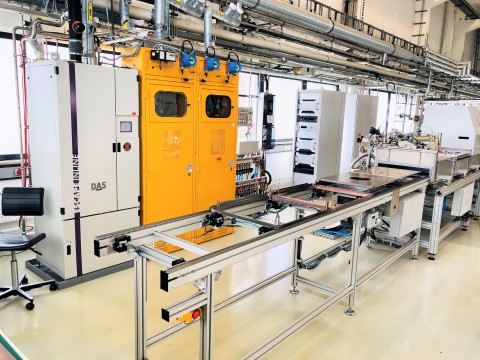
AE’s plasma lab multi-chamber inline coater showing substrate carrier and vacuum load lock in the foreground and with various gas handling cabinets and AE’s power supplies in racks in the background. This equipment includes but is not limited to planar and rotatable dual magnetron sputtering (DMS), and has plasma etch pre-cleaning capability. Various substrate sizes from small experimental coupons (e.g. glass, sapphire, silicon and more) up to 500x600 mm2 rectangular sheets (e.g. glass, plexiglass, plastic, metal and more) can be utilized. (Photo: Business Wire)