Thursday, December 14, 2017

Ultrahigh Elastic Strain Energy Storage in Metal-Oxide-Infiltrated Patterned Hybrid Polymer Nanocomposites

Phys.org reports: A team of scientists from the U.S. Department of Energy's Brookhaven National Laboratory and the University of Connecticut have developed a customizable nanomaterial that combines metallic strength with a foam-like ability to compress and spring back.
 
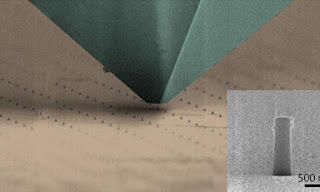
This scanning electron micrograph (SEM) image shows the nanomechanical testing tip passing over the arrays of custom-made nanopillars as it applies pressure to test elasticity and energy storage potential. The inset shows the structure of an individual hybrid nanopillar. Credit: Brookhaven National Laboratory

Read more at: https://phys.org/news/2017-12-scientists-nanoscale-pillars-memory-foam.html#jCp

This scanning electron micrograph (SEM) image shows the nanomechanical testing tip passing over the arrays of custom-made nanopillars as it applies pressure to test elasticity and energy storage potential. The inset shows the structure of an individual hybrid nanopillar. Credit: Brookhaven National Laboratory

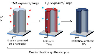
According to the supplemantary information The patterned SU-8 nanopillars were subjected to the AlOx infiltration synthesis at 85 °C using a commercial ALD system (Cambridge Nanotech Savannah S100). TMA (Sigma-Aldrich) was infiltrated into the polymer template for 5 min (vapor pressure <100 Torr), followed by N2 purging of the ALD chamber for 5 min (100 sccm). Then, water vapor was infiltrated into the polymer next for 5 min (pressure < 10 Torr), followed by N2 purging for 5 min, completing one synthesis cycle. A total of up to 16 cycles were applied.

This diagram shows the breakthrough synthesis process developed for these hybrid nanomaterials. First, electron-beam lithography carves the isolated nanopillars, then an aluminum vapor (TMA) infiltrates the pores in the structures, and finally exposure to water creates the final aluminum-oxide infused material. Credit: Brookhaven National Laboratory.

Please finde the abstract from Nanoletters below.
 
Read more at: LINK

Ultrahigh Elastic Strain Energy Storage in Metal-Oxide-Infiltrated Patterned Hybrid Polymer Nanocomposites

Nano Lett., 2017, 17 (12), pp 7416–7423
DOI: 10.1021/acs.nanolett.7b03238

Modulus of resilience, the measure of a material’s ability to store and release elastic strain energy, is critical for realizing advanced mechanical actuation technologies in micro/nanoelectromechanical systems. In general, engineering the modulus of resilience is difficult because it requires asymmetrically increasing yield strength and Young’s modulus against their mutual scaling behavior. This task becomes further challenging if it needs to be carried out at the nanometer scale. Here, we demonstrate organic–inorganic hybrid composite nanopillars with one of the highest modulus of resilience per density by utilizing vapor-phase aluminum oxide infiltration in lithographically patterned negative photoresist SU-8. In situ nanomechanical measurements reveal a metal-like high yield strength (∼500 MPa) with an unusually low, foam-like Young’s modulus (∼7 GPa), a unique pairing that yields ultrahigh modulus of resilience, reaching up to ∼24 MJ/m3 as well as exceptional modulus of resilience per density of ∼13.4 kJ/kg, surpassing those of most engineering materials. The hybrid polymer nanocomposite features lightweight, ultrahigh tunable modulus of resilience and versatile nanoscale lithographic patternability with potential for application as nanomechanical components which require ultrahigh mechanical resilience and strength.

Globalfoundrfies to use quad patterning and Cobalt contacts for 7nm

ZDNet reports: At IEDM Globalfoundries presented details of its 7nm process which promises a significant increase in density, performance and efficiency in comparison to the 14nm technology used to manufacture AMD processors, IBM Power server chips and other products. GlobalFoundries will start 7nm production using current lithography tools, though it plans to quickly move to next-generation EUV lithography to cut costs

Based on GlobalFoundries latest generation of 3D or FinFET transistors, the 7LP process has a fin pitch (the distance between the conducting channels) of 30nm, gate pitch of 56nm and a minimum metal pitch of 40nm--all of which are "significantly scaled from 14nm." GlobalFoundries said it tuned the fin shape and profile for best performance, but did not provide measurements for the width or height of the fins. The smallest high-density SRAM cell measures 0.0269 square microns.
 
Like Intel, GlobalFoundries will use self-aligned quad patterning (SAQP) to fabricate the fins, as well as double-patterning for metal layers, and has introduced cobalt metal contacts to reduce resistance.


Thursday, December 7, 2017

Picosun Oy and Ushio Inc. start collaboration in Japan

ESPOO, Finland, and TOKYO, Japan, 6th December, 2017 – Picosun Oy, a leading supplier of advanced Atomic Layer Deposition (ALD) thin film coating solutions, and Ushio Inc., a leading manufacturer of light sources and optical equipment, have started collaboration to boost the sales of Picosun’s ALD technology in the Japanese market.

Japan has long been one of Picosun’s most important market areas, where the demand for industrial ALD solutions is constantly increasing. In order to always guarantee first-class service to the esteemed customers in the area, Picosun Japan Co. Ltd was established as Picosun’s local subsidiary. Now, to extend this sales and service network even further, Picosun has decided to collaborate with Ushio, with Ushio working as its sales representative. Ushio is a well-known, well-established supplier of a wide variety of manufacturing equipment to the global semiconductor market, and Picosun’s fully automated, SEMI-compliant, and production line compatible industrial ALD systems will be a key addition to their portfolio.

Tuesday, December 5, 2017

Atomic Layer Processing for free!


Journal of Vacuum Science & Technology  is  More than Vacuum

Recent Atomic Layer Processing Articles 


Submit Your Articles on Atomic Layer Processing to JVST 
 
The following articles are free to download for next 30 days:

Quasi-atomic layer etching of silicon nitride
Sonam D. Sherpa and Alok Ranjan
J. Vac. Sci. Technol., A 35, 01A102 (2017) | Read More 
 
Predicting synergy in atomic layer etching
Keren J. Kanarik, Samantha Tan, Wenbing Yang, Taeseung Kim, Thorsten Lill, Alexander Kabansky, Eric A. Hudson, Tomihito Ohba, Kazuo Nojiri, Jengyi Yu, Rich Wise, Ivan L. Berry, Yang Pan, Jeffrey Marks, and Richard A. Gottscho
J. Vac. Sci. Technol., A 35, 05C302 (2017) |  Read More 
 
Atomic layer etching of SiO2 by alternating an O2 plasma with fluorocarbon film deposition
Takayoshi Tsutsumi, Hiroki Kondo, Masaru Hori, Masaru Zaitsu, Akiko Kobayashi, Toshihisa Nozawa, and Nobuyoshi Kobayashi
J. Vac. Sci. Technol., A 35, 01A103 (2017) | Read More 
 
Review Article: Plasma-surface interactions at the atomic scale for patterning metals
Nicholas D. Altieri, Jack Kun-Chieh Chen, Luke Minardi, and Jane P. Chang
J. Vac. Sci. Technol., A 35, 05C203 (2017) |  Read More 
 
Atomic layer etching in close-to-conventional plasma etch tools
Andy Goodyear and Mike Cooke
J. Vac. Sci. Technol., A 35, 01A105 (2017) |  Read More 
 
Correcting defects in area selective molecular layer deposition
Richard G. Closser, David S. Bergsman, Luis Ruelas, Fatemeh Sadat Minaye Hashemi, and Stacey F. Bent
J. Vac. Sci. Technol., A 35, 031509 (2017) | Read More 
 
Revisiting the growth mechanism of atomic layer deposition of Al2O3: A vibrational sum-frequency generation study
Vincent Vandalon and W. M. M. (Erwin) Kessels
J. Vac. Sci. Technol., A 35, 05C313 (2017) | Read More 
 
High-k oxides by atomic layer deposition-Applications in biology and medicine
Marek Godlewski, Sylwia Gierałtowska, Łukasz Wachnicki, Rafał Pietuszka, Bartłomiej S. Witkowski, Anna Słońska, Zdzisław Gajewski, and Michał M. Godlewski
J. Vac. Sci. Technol., A 35, 021508 (2017) |  Read More 
 
Atomic layer deposition of h-BN(0001) on RuO2(110)/Ru(0001)
Jessica Jones, Brock Beauclair, Opeyemi Olanipekun, Sherard Lightbourne, Mofei Zhang, Brittany Pollok, Aparna Pilli, and Jeffry Kelber
J. Vac. Sci. Technol., A 35, 01B139 (2017) |  Read More 
 
Atomic fluorine densities in electron beam generated plasmas: A high ion to radical ratio source for etching with atomic level precision
David R. Boris, Tzvetelina B. Petrova, George M. Petrov, and Scott G. Walton
J. Vac. Sci. Technol., A 35, 01A104 (2017) |  Read More