Showing posts with label MoS2. Show all posts

Monday, October 23, 2023

TSMC To Report Breakthrough in NMOS Nanosheets Using Ultra-Thin MoS2 Channels at IEDM 2023

A TSMC-led research team, in collaboration with National Yang Ming Chiao Tung University and National Applied Research Laboratories, has unveiled promising results for using ultra-thin transition metal dichalcogenides (TMDs), specifically MoS2, as the channel material in NMOS nanosheets. Their innovative approach deviates from the conventional method of thinning Si channels. The team's devices exhibited impressive performance metrics: a positive threshold voltage (VTH) of ~1.0 V, a high on-current of ~370 µA/µm at VDS = 1 V, a large on/off ratio of 1E8, and a low contact resistance ranging between 0.37-0.58 kΩ-µm. These outcomes were primarily attributed to the introduction of a novel C-shaped wrap-around contact, which enhances contact area, and an optimized gate stack. While the devices demonstrated satisfactory mechanical stability, a challenge remains in addressing defect creation within the MoS2 channels. This groundbreaking study, titled "Monolayer-MoS2 Stacked Nanosheet Channel with C-type Metal Contact" by Y-Y Chung et al., is a pivotal step forward in nanosheet scaling using TMDs.


ALD is a the technique for the precise and uniform synthesis of MoS₂, especially for semiconductor applications on large-scale wafers. The choice of precursors plays a crucial role in achieving optimal deposition characteristics. Mo (CO) 6 and H2S have been identified as the primary precursors for depositing molybdenum and sulfur components, respectively. These precursors have demonstrated the capacity for self-limiting growth behavior within a specific ALD temperature window, leading to uniform MoS₂ layers. Notably, this process has been successfully scaled up to achieve highly uniform film growth on large 300 mm SiO2/Si wafers, marking its potential for industry-level manufacturing. The ability to maintain uniformity and thickness control on such wafers emphasizes the potential of ALD in integrating MoS₂ into next-generation electronic devices and further underscores the significance of selecting appropriate precursors for optimal deposition outcomes. Other precursors have been investigated. MoCl₅ and MoF₆ serve as alternative molybdenum sources. For the sulfur component, H₂S is commonly paired with molybdenum precursors, but (CH₃)₂S has also been explored. The choice of these precursors directly impacts the properties of the resulting MoS₂ film in the ALD process and therefore precursor development for 2D MoS2 is a hot field of ongoing research.

While deposition methods are abundant, etching processes are comparatively scarce. Recent research by Elton Graugnard et al also introduces a thermal Atomic Layer Etching (ALE) technique for MoS2, leveraging MoF6 for fluorination, alternated with H2O exposures, to etch both crystalline and amorphous MoS2 films. This process has been characterized using various analytical techniques like QCM, FTIR, and QMS. The etching is temperature-dependent, with a significant increase in mass change per cycle as temperature rises. The mechanism involves two-stage oxidation of Mo, producing volatile byproducts. The resultant etch rates were established for different films, and post-etch annealing rendered crystalline MoS2 films. The thermal MoS2 ALE introduces a promising low-temperature method for embedding MoS2 films in large-scale device manufacturing.


Friday, January 24, 2020

Russian researchers obtain atomically thin molybdenum disulfide (2D) films on large-area substrates by ALD

[Press release: LINK] Researchers from the Moscow Institute of Physics and Technology have managed to grow atomically thin films of molybdenum disulfide spanning up to several tens of square centimeters. It was demonstrated that the material’s structure can be modified by varying the synthesis temperature. The films, which are of interest to electronics and optoelectronics, were obtained at 900-1,000 degrees Celsius. The findings were published in the journal ACS Applied Nano Materials.


An atomic layer deposition reactor from Picosun used for obtaining ultrathin molybdenum oxide films, which were subsequently sulfurized to 2D molybdenum disulfide. Image courtesy of the Atomic Layer Deposition Lab, MIPT

Two-dimensional materials are attracting considerable interest due to their unique properties stemming from their structure and quantum mechanical restrictions. The family of 2D materials includes metals, semimetals, semiconductors, and insulators. Graphene, which is perhaps the most famous 2D material, is a monolayer of carbon atoms. It has the highest charge-carrier mobility recorded to date. However, graphene has no band gap under standard conditions, and that limits its applications.


Monday, June 22, 2015

Penn State - Diode a few atoms thick shows surprising quantum effect

As publish by Penn State : A quantum mechanical transport phenomenon demonstrated for the first time in synthetic, atomically-thin layered material at room temperature could lead to novel nanoelectronic circuits and devices, according to researchers at Penn State and three other U.S. and international universities.


Atomic multilayer structure of van der Waals solids representing layering with a graphene substrate.


Current-voltage curves of single junction (green) van der Waals solid (no NDR) and multijunction (red, orange) van der Waals solids (NDR). Stacking and choice of materials determines the location and width of peak.

The quantum transport effect, called negative differential resistance (NDR), was observed when a voltage was applied to structures made of one-atom-thick layers of several layered materials known as van der Waals materials. The three-part structures consist of a base of graphene followed by atomic layers of either molybdenum disulfide (MoS2), molybdenum diselenide (MoSe2), or tungsten diselenide (WSe2).

NDR is a phenomenon in which the wave nature of electrons allows them to tunnel through any material with varying resistance. The potential of NDR lies in low voltage electronic circuits that could be operated at high frequency.

“Theory suggests that stacking two-dimensional layers of different materials one atop the other can lead to new materials with new phenomena,” said Joshua Robinson, a Penn State assistant professor of materials science and engineering whose student, Yu-Chuan Lin, is first author on a paper appearing online today, June 19, in the journal Nature Communications. The paper is titled “Atomically Thin Resonant Tunnel Diodes Built from Synthetic van der Waals Heterostructures.”

Achieving NDR in a resonant tunneling diode at room temperature requires nearly perfect interfaces, which are possible using direct growth techniques, in this case oxide vaporization of molybdenum oxide in the presence of sulfur vapor to make the MoS2 layer, and metal organic chemical vapor deposition to make the WSe2 and MoSe2.

Monday, May 4, 2015

2D Molybdenum disulfide encapsulated between layers of boron nitride

Beautiful work of 2D material stacks for future electronics - layered stacks of molybdenum disulfide (MoS2) encapsulated in boron nitride (BN), with graphene overlapping the edge of the MoS2 to act as electrical contacts as Published by : Holly Evarts, "Two-Dimensional Semiconductor Comes Clean", Apr. 27, 2015 and in Nature Nanotechnology below.
Bookmark and Share 

In 2013 James Hone, Wang Fong-Jen Professor of Mechanical Engineering at Columbia Engineering, and colleagues at Columbia demonstrated that they could dramatically improve the performance of graphene—highly conducting two-dimensional (2D) carbon—by encapsulating it in boron nitride (BN), an insulating material with a similar layered structure. In work published this week in the Advance Online Publication on Nature Nanotechnology’s website, researchers at Columbia Engineering, Harvard, Cornell, University of Minnesota, Yonsei University in Korea, Danish Technical University, and the Japanese National Institute of Materials Science have shown that the performance of another 2D material—molybdenum disulfide (MoS2)—can be similarly improved by BN-encapsulation.


Two-dimensional semiconductor comes clean 

Schematic cross-section view of atomic layer of molybdenum disulfide contacted by graphene, and encapsulated between layers of insulating hexagonal boron nitride. Credit: Gwan-Hyoung Lee/Columbia Engineering

Read more at: http://phys.org/news/2015-04-two-dimensional-semiconductor.html#jCp
Molybdenum disulfide encapsulated between layers of boron nitride (Image courtesy of Gwan-Hyoung Lee/Yonsei University).
Schematic cross-section view of atomic layer of molybdenum disulfide contacted by graphene, and encapsulated between layers of insulating hexagonal boron nitride. Credit: Gwan-Hyoung Lee/Columbia Engineering

Read more at: http://phys.org/news/2015-04-two-dimensional-semiconductor.html#jCp
Schematic cross-section view of atomic layer of molybdenum disulfide contacted by graphene, and encapsulated between layers of insulating hexagonal boron nitride. Credit: Gwan-Hyoung Lee/Columbia Engineering

Read more at: http://phys.org/news/2015-04-two-dimensional-semiconductor.html#jCp
Schematic cross-section view of atomic layer of molybdenum disulfide contacted by graphene, and encapsulated between layers of insulating hexagonal boron nitride. Credit: Gwan-Hyoung Lee/Columbia Engineering

Read more at: http://phys.org/news/2015-04-two-dimensional-semiconductor.html#jCp

Schematic cross-section view of atomic layer of molybdenum disulfide contacted by graphene, and encapsulated between layers of insulating hexagonal boron nitride. Credit: Gwan-Hyoung Lee/Columbia Engineering

“These findings provide a demonstration of how to study all 2D materials,” says Hone, leader of this new study and director of Columbia’s NSF-funded Materials Research Science and Engineering Center. “Our combination of BN and graphene electrodes is like a ‘socket’ into which we can place many other materials and study them in an extremely clean environment to understand their true properties and potential. This holds great promise for a broad range of applications including high-performance electronics, detection and emission of light, and chemical/bio-sensing.”

Two-dimensional (2D) materials created by “peeling’” atomically thin layers from bulk crystals are extremely stretchable, optically transparent, and can be combined with each other and with conventional electronics in entirely new ways. But these materials—in which all atoms are at the surface—are by their nature extremely sensitive to their environment, and their performance often falls far short of theoretical limits due to contamination and trapped charges in surrounding insulating layers. The BN-encapsulated graphene that Hone’s group produced last year has 50× improved electronic mobility—an important measure of electronic performance—and lower disorder that enables the study of rich new phenomena at low temperature and high magnetic fields.

“We wanted to see what we could do with MoS2—it’s the best-studied 2D semiconductor, and, unlike graphene, it can form a transistor that can be switched fully ‘off’, a property crucial for digital circuits,” notes Gwan-Hyoung Lee, co-lead author on the paper and assistant professor of materials science at Yonsei. In the past, MoS2 devices made on common insulating substrates such as silicon dioxide have shown mobility that falls below theoretical predictions, varies from sample to sample, and remains low upon cooling to low temperatures, all indications of a disordered material. Researchers have not known whether the disorder was due to the substrate, as in the case of graphene, or due to imperfections in the material itself.

In the new work, Hone’s team created heterostructures, or layered stacks, of MoS2 encapsulated in BN, with small flakes of graphene overlapping the edge of the MoS2 to act as electrical contacts. They found that the room-temperature mobility was improved by a factor of about 2, approaching the intrinsic limit. Upon cooling to low temperature, the mobility increased dramatically, reaching values 5-50× that those measured previously (depending on the number of atomic layers). As a further sign of low disorder, these high-mobility samples also showed strong oscillations in resistance with magnetic field, which had not been previously seen in any 2D semiconductor.

“This new device structure enables us to study quantum transport behavior in this material at low temperature for the first time,” added Columbia Engineering PhD student Xu Cui, the first author of the paper.

By analyzing the low-temperature resistance and quantum oscillations, the team was able to conclude that the main source of disorder remains contamination at the interfaces, indicating that further improvements are possible.

“This work motivates us to further improve our device assembly techniques, since we have not yet reached the intrinsic limit for this material,” Hone says. “With further progress, we hope to establish 2D semiconductors as a new family of electronic materials that rival the performance of conventional semiconductor heterostructures—but are created using scotch tape on a lab-bench instead of expensive high-vacuum systems.”

Multi-terminal transport measurements of MoS2 using a van der Waals heterostructure device platform
Xu Cui, Gwan-Hyoung Lee, Young Duck Kim, Ghidewon Arefe, Pinshane Y. Huang, Chul-Ho Lee, Daniel A. Chenet, Xian Zhang, Lei Wang, Fan Ye, Filippo Pizzocchero, Bjarke S. Jessen, Kenji Watanabe, Takashi Taniguchi, David A. Muller, Tony Low, Philip Kim & James Hone
Nature Nanotechnology(2015)doi:10.1038/nnano.2015.70
Schematic cross-section view of atomic layer of molybdenum disulfide contacted by graphene, and encapsulated between layers of insulating hexagonal boron nitride. Credit: Gwan-Hyoung Lee/Columbia Engineering

Read more at: http://phys.org/news/2015-04-two-dimensional-semiconductor.html#jCp
Schematic cross-section view of atomic layer of molybdenum disulfide contacted by graphene, and encapsulated between layers of insulating hexagonal boron nitride. Credit: Gwan-Hyoung Lee/Columbia Engineering

Read more at: http://phys.org/news/2015-04-two-dimensional-semiconductor.html#jCp
Schematic cross-section view of atomic layer of molybdenum disulfide contacted by graphene, and encapsulated between layers of insulating hexagonal boron nitride. Credit: Gwan-Hyoung Lee/Columbia Engineering

Read more at: http://phys.org/news/2015-04-two-dimensional-semiconductor.html#jCp
Schematic cross-section view of atomic layer of molybdenum disulfide contacted by graphene, and encapsulated between layers of insulating hexagonal boron nitride. Credit: Gwan-Hyoung Lee/Columbia Engineering

Read more at: http://phys.org/news/2015-04-two-dimensional-semiconductor.html#jCp
Schematic cross-section view of atomic layer of molybdenum disulfide contacted by graphene, and encapsulated between layers of insulating hexagonal boron nitride. Credit: Gwan-Hyoung Lee/Columbia Engineering

Read more at: http://phys.org/news/2015-04-two-dimensional-semiconductor.html#jCp


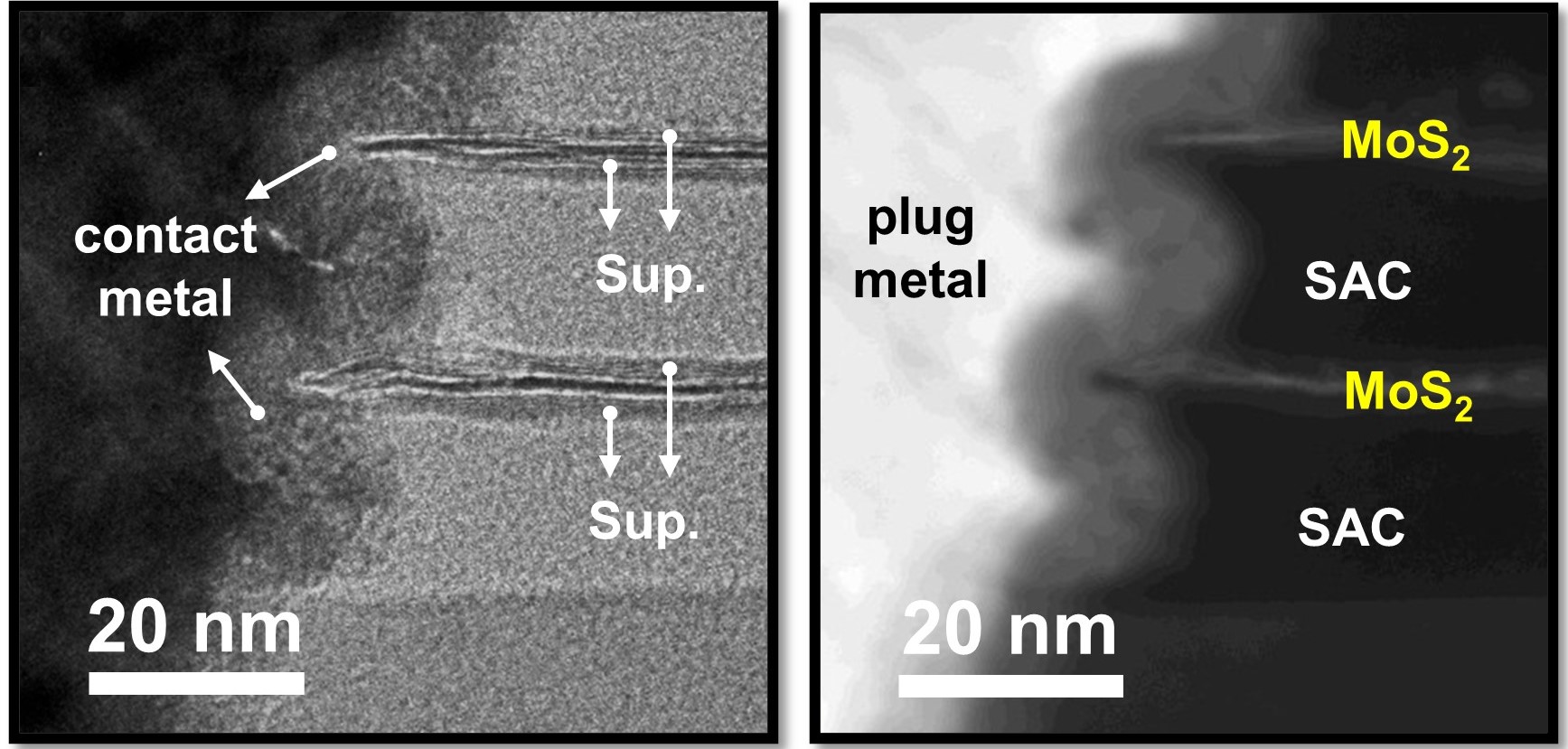
Figure 1c: Cross-sectional STEM image of the fabricated device. The zoom-in false-colour image clearly shows the ultra-sharp interfaces between different layers (graphene, 5L; MoS2, 3L;top hBN, 8nm; bottom hBN, 19 nm) [Figure and Abstract used with permission from Nature Publishing Group under License Number 3621820766388]

Atomically thin two-dimensional semiconductors such as MoS2 hold great promise for electrical, optical and mechanical devices and display novel physical phenomena. However, the electron mobility of mono- and few-layer MoS2 has so far been substantially below theoretically predicted limits, which has hampered efforts to observe its intrinsic quantum transport behaviours. Potential sources of disorder and scattering include defects such as sulphur vacancies in the MoS2 itself as well as extrinsic sources such as charged impurities and remote optical phonons from oxide dielectrics. To reduce extrinsic scattering, we have developed here a van der Waals heterostructure device platform where MoS2 layers are fully encapsulated within hexagonal boron nitride and electrically contacted in a multi-terminal geometry using gate-tunable graphene electrodes. Magneto-transport measurements show dramatic improvements in performance, including a record-high Hall mobility reaching 34,000 cm2 V–1 s–1 for six-layer MoS2 at low temperature, confirming that low-temperature performance in previous studies was limited by extrinsic interfacial impurities rather than bulk defects in the MoS2. We also observed Shubnikov–de Haas oscillations in high-mobility monolayer and few-layer MoS2. Modelling of potential scattering sources and quantum lifetime analysis indicate that a combination of short-range and long-range interfacial scattering limits the low-temperature mobility of MoS2.

Wednesday, May 21, 2014

Hybrid technology for 2D electronics by graphene/molybdenum disulfide heterostructures grown by CVD

Nanotechweb.org reports that Researchers in the US have unveiled a new CMOS-compatible technology to integrate different two-dimensional materials into a single electronic device. The team, led by Tomás Palacios of the Massachusetts Institute of Technology, constructed large-scale electronic circuits based on graphene and molybdenum sulphide heterostructures grown by chemical vapour deposition where MoS2 was used as a transistor channel, and graphene as contact electrodes and circuit interconnects. The fabrication process itself might be extended to fabricate heterostructures from any type of 2D layered material with potential applications in flexible and transparent electronics, sensors, tunnelling FETs and high-electron mobility transistors.
 
Demonstration of a novel technology for constructing large-scale electronic systems based on graphene/molybdenum disulfide (MoS2) heterostructures grown by chemical vapor deposition.
 
Mor details on this work in the article below:
 
Lili Yu, Yi-Hsien Lee, Xi Ling, Elton J. G. Santos, Yong Cheol Shin , Yuxuan Lin, Madan Dubey, Efthimios Kaxiras, Jing Kong, Han Wang, and Tomás Palacios
Nano Lett., DOI: 10.1021/nl404795z Publication Date (Web): May 8, 2014

Abstract: Two-dimensional (2D) materials have generated great interest in the past few years as a new toolbox for electronics. This family of materials includes, among others, metallic graphene, semiconducting transition metal dichalcogenides (such as MoS2), and insulating boron nitride. These materials and their heterostructures offer excellent mechanical flexibility, optical transparency, and favorable transport properties for realizing electronic, sensing, and optical systems on arbitrary surfaces. In this paper, we demonstrate a novel technology for constructing large-scale electronic systems based on graphene/molybdenum disulfide (MoS2) heterostructures grown by chemical vapor deposition. We have fabricated high-performance devices and circuits based on this heterostructure, where MoS2 is used as the transistor channel and graphene as contact electrodes and circuit interconnects. We provide a systematic comparison of the graphene/MoS2 heterojunction contact to more traditional MoS2-metal junctions, as well as a theoretical investigation, using density functional theory, of the origin of the Schottky barrier height. The tunability of the graphene work function with electrostatic doping significantly improves the ohmic contact to MoS2. These high-performance large-scale devices and circuits based on this 2D heterostructure pave the way for practical flexible transparent electronics.