Showing posts with label IEDM. Show all posts

Saturday, October 26, 2024

Intel's Breakthrough in RibbonFET Transistor Scaling Demonstrates Silicon Viability for Future Nodes

For the latest insights from the 2024 IEEE International Electron Devices Meeting (IEDM), including groundbreaking advancements in 2nm CMOS logic, extremely scaled transistors, monolithic CFET inverters, energy-efficient 3D computing-in-memory, and novel device technologies, you can explore the full press kit here.

Extremely Scaled Transistors from Intel: Intel researchers will show that silicon can continue to support the extreme gate length scaling which future technology nodes require. They will describe how they built RibbonFET CMOS transistors (Intel’s version of nanosheets) with 6nm gate lengths at 45nm contacted poly pitch (CPP, the spacing between adjacent transistor gates), with no degradation of electron mobility (how fast electrons can move through a material). The researchers will show that electron mobility doesn’t degrade until 3nm Tsi (silicon thickness), below which electron scattering due to surface roughness becomes an issue. They will describe how they achieved good short channel control (≤100mV/V at <4nm Tsi), with extremely low threshold voltage at these gate lengths through clever workfunction engineering. The work shows that 3nm is a practical scaling limit for RibbonFETs.


The image illustrates the behavior of drain-induced barrier lowering (DIBL) vs. silicon thickness (Tsi) at LG=18nm. It shows a reduction as Tsi is scaled from 10nm to 1.5nm; however, DIBL reduction saturates at Tsi <4nm, below which very little gain is obtained. PMOS DIBL is elevated vs. NMOS DIBL at the same Tsi. Also shown are TEM micrographs of a 1NR transistor with various Tsi values down to 1.5nm.


The series of images are (a) TEM micrograph and EDX scan of a completed 6nm RibbonFET device on a 1NR vehicle, showing a disconnected subfin; (b - d) are high-resolution cross-section TEMs for Tsi=5.5nm, 3.1nm and 1.7nm respectively, at 6nm gate length on a 1NR vehicle

Sources:
IEDM 2024 Press Kit Paper #2.2, “Silicon RibbonFET CMOS at 6nm Gate Length,” A. Agrawal et al, Intel https://www.ieee-iedm.org/press-kit

TSMC 2nm Platform Technology Featuring Energy-Efficient Nanosheet Transistors and Interconnects

TSMC’s New, Industry-Leading 2nm CMOS Logic Platform: In a late-news paper, TSMC researchers will unveil the world’s most advanced logic technology. It is the company’s forthcoming 2nm CMOS (i.e., N2), platform, designed for energy-efficient computing in AI, mobile, and HPC applications. It offers a 15% speed gain (or 30% power reduction) at >1.15x chip density versus the most advanced logic technology currently in production, TSMC’s own 3nm CMOS (N3) platform, introduced in late 2022.

The new N2 platform features GAA nanosheet transistors; middle-/back-end-of-line interconnects with the densest SRAM macro ever reported (~38Mb/mm2); and a holistic, system-technology co-optimized (STCO) architecture offering great design flexibility. That architecture includes a scalable copper-based redistribution layer and a flat passivation layer (for better performance, robust CPI, and seamless 3D integration); and through-silicon vias, or TSVs (for power/signal with F2F/F2B stacking). The researchers say the N2 platform is currently in risk production and scheduled for mass production in 2H’ 25. N2P (5% speed enhanced version of N2) targets to complete qualification in 2025 and mass production in 2026.


The cross-sectional image shows that the N2 platform’s Cu redistribution layer (RDL) and passivation provide seamless integration with 3D technologies.


Graph showing that the new N2 high-density cells gain 14~15% speed@power vs. N3E FinFlex 2-1 fin cells across the Vdd range; a 35% power savings at higher voltage; and a 24% power savings at lower voltage

The graph above compares two CMOS technology nodes, TSMC's N3E and N2, specifically for Arm's A715 core. N3E FinFlex (2-1 Fin) architecture, represented by the blue dotted line, operates at higher power but achieves higher speed than previous nodes. Operating at voltages between 0.5V and 0.9V, the N3E design can achieve significant performance levels but comes with a power increase. Now, N2 NanoFlex HD (High-Density) Energy-Efficient Cells as in the The N2 node, marked by the green dotted line, introduces "NanoFlex" cells that are optimized for energy efficiency. Compared to N3E, it achieves similar speeds but with substantially lower power consumption, marking a shift toward lower power designs in advanced nodes.

Key Improvements:
  • When shifting from 0.6V to 0.55V in the N3E architecture, there's a 15% reduction in speed but a 24% reduction in power.
  • For N2, at 0.85V, there's a 14% reduction in speed and a 35% reduction in power compared to similar performance points in N3E.
  • These efficiency improvements are essential for high-performance applications in power-sensitive environments.

In summary, TSMC's N3E focuses on performance with FinFlex technology, while N2's NanoFlex HD cells target power efficiency, marking a clear trend in CMOS architecture evolution for balancing power and speed.

For the latest insights from the 2024 IEEE International Electron Devices Meeting (IEDM), including groundbreaking advancements in 2nm CMOS logic, extremely scaled transistors, monolithic CFET inverters, energy-efficient 3D computing-in-memory, and novel device technologies, you can explore the full press kit here.


Sources: 

IEDM Press kit Paper #2.1, “2nm Platform Technology Featuring Energy-Efficient Nanosheet Transistors and Interconnects Co-Optimized with 3DIC for AI, HPC and Mobile SoC Applications,” G. Yeap et al, TSMC https://www.ieee-iedm.org/press-kit


Monday, October 23, 2023

TSMC To Report Breakthrough in NMOS Nanosheets Using Ultra-Thin MoS2 Channels at IEDM 2023

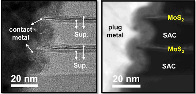
A TSMC-led research team, in collaboration with National Yang Ming Chiao Tung University and National Applied Research Laboratories, has unveiled promising results for using ultra-thin transition metal dichalcogenides (TMDs), specifically MoS2, as the channel material in NMOS nanosheets. Their innovative approach deviates from the conventional method of thinning Si channels. The team's devices exhibited impressive performance metrics: a positive threshold voltage (VTH) of ~1.0 V, a high on-current of ~370 µA/µm at VDS = 1 V, a large on/off ratio of 1E8, and a low contact resistance ranging between 0.37-0.58 kΩ-µm. These outcomes were primarily attributed to the introduction of a novel C-shaped wrap-around contact, which enhances contact area, and an optimized gate stack. While the devices demonstrated satisfactory mechanical stability, a challenge remains in addressing defect creation within the MoS2 channels. This groundbreaking study, titled "Monolayer-MoS2 Stacked Nanosheet Channel with C-type Metal Contact" by Y-Y Chung et al., is a pivotal step forward in nanosheet scaling using TMDs.


ALD is a the technique for the precise and uniform synthesis of MoS₂, especially for semiconductor applications on large-scale wafers. The choice of precursors plays a crucial role in achieving optimal deposition characteristics. Mo (CO) 6 and H2S have been identified as the primary precursors for depositing molybdenum and sulfur components, respectively. These precursors have demonstrated the capacity for self-limiting growth behavior within a specific ALD temperature window, leading to uniform MoS₂ layers. Notably, this process has been successfully scaled up to achieve highly uniform film growth on large 300 mm SiO2/Si wafers, marking its potential for industry-level manufacturing. The ability to maintain uniformity and thickness control on such wafers emphasizes the potential of ALD in integrating MoS₂ into next-generation electronic devices and further underscores the significance of selecting appropriate precursors for optimal deposition outcomes. Other precursors have been investigated. MoCl₅ and MoF₆ serve as alternative molybdenum sources. For the sulfur component, H₂S is commonly paired with molybdenum precursors, but (CH₃)₂S has also been explored. The choice of these precursors directly impacts the properties of the resulting MoS₂ film in the ALD process and therefore precursor development for 2D MoS2 is a hot field of ongoing research.

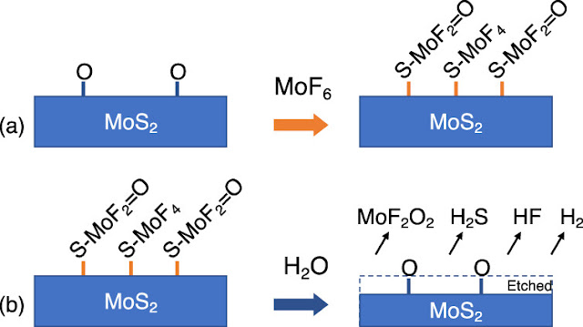
While deposition methods are abundant, etching processes are comparatively scarce. Recent research by Elton Graugnard et al also introduces a thermal Atomic Layer Etching (ALE) technique for MoS2, leveraging MoF6 for fluorination, alternated with H2O exposures, to etch both crystalline and amorphous MoS2 films. This process has been characterized using various analytical techniques like QCM, FTIR, and QMS. The etching is temperature-dependent, with a significant increase in mass change per cycle as temperature rises. The mechanism involves two-stage oxidation of Mo, producing volatile byproducts. The resultant etch rates were established for different films, and post-etch annealing rendered crystalline MoS2 films. The thermal MoS2 ALE introduces a promising low-temperature method for embedding MoS2 films in large-scale device manufacturing.


Saturday, October 21, 2023

Intel Unveils Breakthrough 3D CFET Design at IEDM: Setting the Stage for Next-Gen Compact and Efficient Electronics

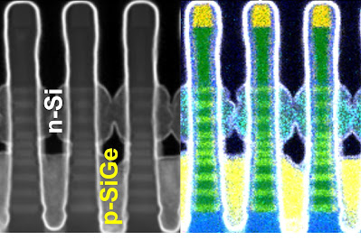
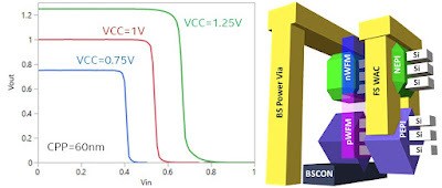
Intel researchers developed a 3D monolithic CFET device* with 3 n-FET nanoribbons atop 3 p-FET nanoribbons, separated by 30 nm gap. This industry-first device enabled the creation of functional inverters at a 60 nm gate pitch. Notably, it incorporated vertically stacked dual-Source/Drain epitaxy, dual metal work function gate stacks, and backside power delivery with direct device contacts. They also introduced a nanoribbon "depopulation" method for varying n-MOS/p-MOS device numbers. This research advances the understanding of CFET scalability for logic and SRAM applications and highlights key process enablers. The paper will be presented at the upcoming IEDM conference in San Francisco.

Comment: The stacked CMOS inverter at a 60 nm gate pitch represents an advancement in semiconductor design, allowing for denser circuits. The 60 nm distance between gates indicates a highly miniaturized design. Power vias provide vertical power connections to different layers, while direct backside device contacts enhance efficiency and heat dissipation. This development offers a glimpse into the  future electronic devices being more compact, efficient, and high-performing than deploying "planar" designs in one layer like the FinFETs and GAA-FETs of today.

ALD plays a key role in manufacturing 3D monolithic CFET devices by assisting in crafting the architecture and providing atomically precise and even thin film layers at small scales. ALD ensures even coverage, which is important for 3D designs, especially on vertical areas and inside deep gaps. It's used to put down important materials in transistor gate stacks (High-k/Metal Gates or HKMG), as well as barrier and seed layers. ALD also helps in doping (SSD - solid state doping), which changes how semiconductors behave, and in creating spacers, important for separating and defining parts of transistors. In brief, ALD helps improve the CFET design and its overall performance.


Figures from IEDM press kit

* A 3D monolithic CFET device combines three-dimensional stacking and the Complementary Field-Effect Transistor (CFET) design within a single semiconductor structure. This approach vertically integrates both n-type and p-type transistors on the same substrate, promoting tighter integration and reduced interconnect delays. By leveraging the complementary operation of CFET and the benefits of 3D stacking, the device aims to enhance performance, miniaturization, and efficiency in semiconductor technology.

Friday, November 30, 2018

ASM International will host a technical luncheon seminar in IEDM 2018 San Francisco, CA, US, on Tuesday, December 4

ASM International N.V. (Euronext Amsterdam: ASM) today announces that it will host a technical luncheon seminar in San Francisco, CA, US, on Tuesday, December 4, 2018, the second day of the IEDM Conference.

At this technology seminar ASM will highlight the challenges and potential solutions for advanced ALD processes, equipment and productivity.

The agenda is as follows:
11:30 am Reception,food and drinks
11:55 - 12:00 pm Dr. Ivo Raaijmakers (ASM) - Welcome and introduction
12:00 - 12:30 pm Speaker: SH Hong, MSc (ASM) - "ALD for Advanced Memories"
12:30 - 1:00 pm Invited speaker: Dr. Bala Haran (IBM) - "Materials Need for the Next Era of Computing


Friday, November 9, 2018

Imec to present scaled Superduper High-k Ruthenium/Strontium titanate capacitor at IEDM

Here is another interesting IEDM 2018 paper from Imec. It is a classical paper obn DRAM capacitor scaling featuring the almost impossible Superduper High-k Ruthenium/Strontium titanate capacitor! It is an ALD integration, the patterning the capacitor everything - no need to involve anyone else - it is up to the Litho and ALD people to get the job done.

Paper #2.7, "High-Performance (EOT<0.4nm, Jg~10-7 A/cm2) ALD-Deposited Ru/SrTiO3 Stack for Next-Generation DRAM Pillar Capacitor," M. Popovici et al, Imec)

I have not seen the abstract but it has been reviewed by CDRInfo (see paragraph below) and I am sure there will be more details available soon (LINK):

"Scaling DRAM Technology To 16nm And Beyond: DRAM memory technology is used in virtually all electronic systems because of its speed and density. DRAM memory comprises arrays of capacitor-transistor pairs which store data as electrical charge in the capacitor; the presence of charge indicates "1" and its absence "0." Manipulation of these digits is the basis of computer programming. It’s difficult to scale DRAM to the 16nm generation and beyond because of space limitations which make it hard to pack enough capacitance within the pitch. Imec researchers used an atomic layer deposition (ALD) process to pattern and build a novel 11nm pillar-shaped capacitor using new dielectric materials (SrTiO3, or STO). By tailoring the material properties of the capacitor and the SrRuO3 (SRO) epitaxial template on which it was grown, the researchers achieved a very high dielectric constant (k~118) and low electrical leakage (10-7 A/cm2 at ±1V). This means that pillar-shaped capacitors can be used instead of existing cup-shaped capacitors, without paying too great a penalty in terms of reduced data-storage capability. These results make the STO capacitors suitable for continued scaling for 16nm and smaller DRAMs."
 
 
Construction work at Imec, Leuven, June 2013. The tower looks a bit like a DRAM Capacitor but somehow I do not think that the architect know that and I bet they were working on Ru/STO ALD well before that!

Samsung will give insights to their 3nm CMOS technology at IEDM2018

The 64th IEDM conference will be held December 1-5, 2018 in San Francisco (LINK). This year Samsung will give insights to their 3nm CMOS technology that will feature the so calle gate-all-around (GAA) transistors. The GAA is trasistors ar realized by having channels made from horizontal layers of nanosheets that are completely surrounded by gate structures. 

Samsung has recently stated (LINK) that they have started wafer production on its new 7LPP node (FinFET). According to the press release the process uses EUV lithography technology and demonstrates that Samsung's Foundry can follow its roadmap reaching down to 3 nm.


Samsung Foundry Roadmap as shown at SFF Japan 2018.
 
Samsung refers to this architecture as a Multi-Bridge-Channel architecture, and claims "that it is highly manufacturable as it makes use of ~90% of the company’s existing FinFET fabrication technology, requiring only a few revised photomasks" (LINK). 
 
Paper #28.7, "3nm GAA Technology Featuring Multi-Bridge-Channel FET for Low-Power and High-Performance Applications," G. Bae et al, Samsung


Sunday, October 22, 2017

Intel to present 10 nm Logic with 3rd gen FinFET and 2 level Cobalt interconnect

IEDM 2017 Announcement (LINK, Press kit): Intel researchers will present a 10nm logic technology platform with excellent transistor and interconnect performance and aggressive design-rule scaling. They demonstrated its versatility by building a 204Mb SRAM having three different types of memory cells: a high-density 0.0312µm2 cell, a low voltage 0.0367µm2 cell, and a high-performance 0.0441µm2 cell. The platform features 3rd-generation FinFETs fabricated with self-aligned quadruple patterning (SAQP) for critical layers, leading to a 7nm fin width at a 34nm pitch, and a 46nm fin height; a 5th-generation high-k metal gate; and 7th-generation strained silicon. There are 12 metal layers of interconnect, with cobalt wires in the lowest two layers that yield a 5-10x improvement in electromigration and a 2x reduction in via resistance. NMOS and PMOS current is 71% and 35% greater, respectively, compared to 14nm FinFET transistors. Metal stacks with four or six workfunctions enable operation at different threshold voltages, and novel self-aligned gate contacts over active gates are employed.

The graph on the left shows that the new platform maintains traditional scaling trends, while the photomicrograph on the right shows the platform’s 12-layer interconnect stack.


Reference: Paper 29.1, “A 10nm High Performance and Low-Power CMOS Technology Featuring 3rd-Generation FinFET Transistors, Self-Aligned Quad Patterning, Contact Over Active Gate and Cobalt Local Interconnects,” C. Auth et al, Intel

2017 IEEE International Electron Devices Meeting
December 2-6, 2017
Hilton San Francisco Union Square
333 O’Farrell Street
San Francisco, CA 94102